Article

An Ultrasonic Through-Metal-Wall Power Transfer System with Regulated DC Output

1
Key Laboratory of Noise and Vibration Research, Institute of Acoustics, Chinese Academy of Sciences, No. 21 North 4th Ring Road, Haidian District, Beijing 100190, China
2
School of Electronic, Electrical and Communication Engineering, University of Chinese Academy of Sciences, No.19(A) Yuquan Road, Shijingshan District, Beijing 100049, China
*
Author to whom correspondence should be addressed.
Appl. Sci. 2018, 8(5), 692; https://doi.org/10.3390/app8050692
Submission received: 13 February 2018 / Revised: 22 April 2018 / Accepted: 26 April 2018 / Published: 29 April 2018

Abstract

:

Featured Application

Wirelessly powering sensors and circuits enclosed in hermetic metal containers.

Abstract

This paper presents a novel and efficient system capable of transmitting medium-power electric energy through a solid metal wall and generating a regulated direct current (DC) output. The electric power is transmitted using radio frequency (RF) ultrasound without physical penetration. An RF alternating current to direct current converter with input impedance matching is used to convert the transmitted RF signal to a DC output, which is directly suitable as a power supply for electronic devices. The system is constructed from commercial off-the-shelf components, and a computer-controlled measurement method is designed to test the effectiveness of the full system. The measurement results show that the system is able to transfer power through a 40-mm-thick stainless steel plate and generate 5-V, 15.7-W regulated DC output power with an overall power transfer efficiency of 27.7%. In addition, the effectiveness of the system is successfully demonstrated by powering ARM® evaluation boards with liquid-crystal display panels. A discussion of potential enhancements that could be made to improve the transfer capability and efficiency of the system is also presented. This system could be applied to improve safety and preserve structural integrity in many industrial and military applications, such as submarines, space crafts, planes, nuclear storage facilities, etc.

1. Introduction

Wireless power transfer (WPT) systems allow elimination of cables, plugs and sockets, resulting in extended maintenance-free operation and increased reliability and safety [1]. In recent years, WPT became a hot topic due to the rapid growth of mobile devices and electric vehicles [2]. A great number of existing WPT systems utilize electromagnetic transmission techniques, but the effectiveness of these approaches in applications containing sealed metal containers (such as submarines, space crafts, planes, nuclear storage facilities, etc.) is limited by the Faraday shielding effect or the skin effect.
As a kind of mechanical wave, ultrasound can penetrate metal walls. So, ultrasound has been suggested as effective means for passing power, as well as data, through metal barriers without physical penetration [3,4,5]. Ultrasound has also been demonstrated capable of safely and efficiently transferring energy through human tissue to power deeply implanted medical devices [6,7,8,9]. In addition, airborne ultrasound has been shown to be a feasible alternative to microwave, capacitive or inductive coupling methods to transfer power wirelessly in air, when the transfer distance is above several times the transducer size [10,11]. However, ultrasonic through-metal-wall power transfer (UTMWPT) systems usually achieve higher power transfer efficiency than ultrasonic through-air or through-non-metal-wall WPT systems, because the acoustic impedance of ultrasonic transducers is better matched to that of metal than air, non-metal or human tissue [12].
In general, a UTMWPT system uses a pair of piezoelectric transducers bonded on the opposite sides of the metal wall to generate and receive ultrasound. Besides, transducers in UTMWPT systems usually operate at frequencies between tens of kHz and 1 MHz, which range from the very low frequency (VLF) band through medium frequency (MF) band of radio spectrum [13].
An analytical solution for UTMWPT systems was proposed by Hu et al., as early as 2003 [3]. In their later work [14], an alternating current to direct current (AC-DC) converter was employed at the receiving side of a UTMWPT system to convert the radio frequency (RF) alternating current (AC) output of the receiving transducer into a stable direct current (DC). The AC-DC converter was composed of a capacitor-filtered diode full-bridge rectifier (CF-DFBR) and a buck DC-DC converter. A rechargeable battery was applied at the output port of the AC-DC converter to store the transmitted energy. In addition, a synchronized switch harvesting on inductor (SSHI) in parallel with the receiving transducer was introduced to extend the closed interval of the AC-DC converter. Both analytical and numerical results of the system were presented. However, no experiments were shown and the system was greatly simplified that the electrodes of the piezoelectric transducers were considered as the metal wall.
Bao et al., presented two UTMWPT systems successively, which could transmit electric powers up to 100 W and 1 kW, respectively, through several-millimetre-thick titanium plates and light incandescent bulbs [15,16]. The operating frequencies of these two UTMWPT systems are 747 kHz and 24.5 kHz, respectively. However, without the use of AC-DC converters, the output of these two UTMWPT systems was not directly suitable as a power supply for electronic circuits because of the high frequencies.
Lawry et al., presented a UTMWPT system with a CF-DFBR as an AC-DC converter [17,18]. The transducers operated at about 1 MHz. The thickness of the metal wall in the system reached up to 63.5 mm; and the material of it was steel, which was more widely used than titanium. Lawry et al. used simultaneous conjugate matching in their system to improve its power transfer efficiency. However, significant power mismatch loss was still caused by the CF-DFBR. DC power of about 19 W was output to a 50 Ω resistor with an efficiency of only about 19%.
Leung et al. proposed a theoretical modeling method to accurately determine the maximum power transfer condition of a UTMWPT system when driving a resistive load [19,20]. The simulation results showed a good consistency in trend with the experimental measurements. They also presented a spider clamp attachment method to bond the piezoelectric transducers to the metal wall in a UTMWPT system [21]. A prototype system built with this new attachment method was shown, which could, at best, transmit 1.0 W of power through a 1-mm-thick steel plate with an efficiency of 38%.
To the best of the authors’ knowledge, no UTMWPT system has been capable of generating a medium-power regulated DC output with a high overall efficiency. Besides, the ability of UTMWPT systems to drive medium-power electronic appliances has not been demonstrated. Therefore, we developed a novel and efficient UTMWPT system. Based on the achievements of Lawry et al. we for the first time adopted an RF AC-DC converter with input impedance matching in a UTMWPT system. This RF AC-DC converter made our UTMWPT system the first one capable of efficiently converting the transmitted RF signal to a regulated DC voltage. We also designed a computer-controlled measurement method to accurately test the effectiveness of the full system. In addition, we successfully demonstrated the system using real electronic appliances–ARM® Cortex™-A8 evaluation boards with liquid-crystal display (LCD) panels.
The paper is organized as follows: Section 2 describes the methods used to design the system. Section 3 describes the computer-controlled measurement method, discusses the measurement results and presents the demonstration experiment. Section 4 draws the conclusions.

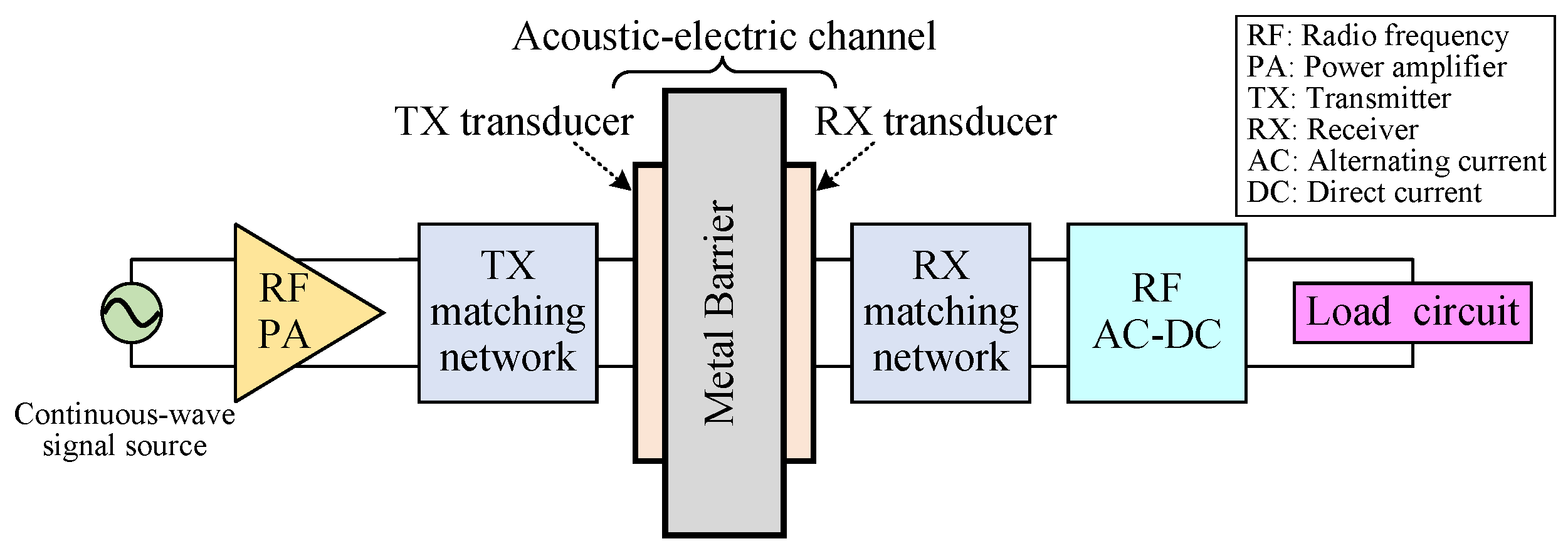
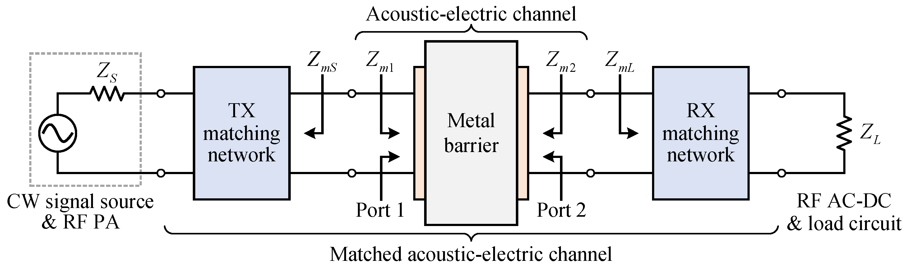
2. System Description

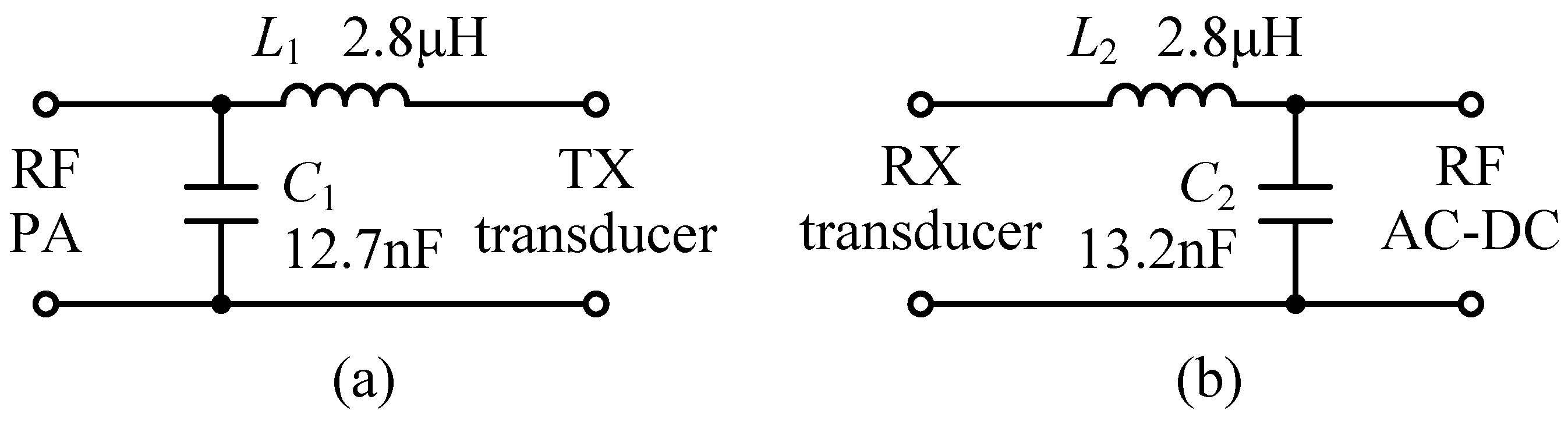
2.1. Acoustic-Electric Channel

Figure 1 shows a block diagram of the full system. The acoustic-electric channel is composed of two commercial PZT-5 piezoelectric disc transducers (Hongsheng Acoustics Co., Baoding, Hebei, China) and a 304 stainless steel plate (dimensions 300 mm × 300 mm × 40 mm ). The transducers are co-axially aligned on opposite sides of the steel plate and bonded to its largest faces using Araldite 2014 epoxy (Huntsman International LLC., the Woodlands, TX, USA). The transducers are both 2 mm thick, which gives them thickness-mode resonance at about 1 MHz. In addition, the diameters of the transducers are both 80 mm.
The exact resonant frequencies of the transducers were measured using a 4294A impedance analyzer (Keysight Technologies Inc., Santa Rosa, CA, USA) before they were bonded to the steel plate, and the results are presented in Figure 2. The resonant frequencies of the transmitter (TX) transducer and the receiver (RX) transducer are 945 kHz and 946.25 kHz, respectively. At the resonant frequencies, the magnitude of the impedances of the transducers has the minimum values [22]. Figure 2 also shows that the quality factor (Q) values of the transducers are smaller than unit at the resonant frequencies. The low Q values make the system high-loss but reduce the resonant frequency consistency requirements on the TX and RX transducers [17].
The TX transducer is driven by the cascaded combination of a continuous-wave (CW) signal source and a 100-W linear RF power amplifier (PA) from Xinpin Technologies LLC (Shenzhen, Guangdong, China). The RX transducer picks up the transmitted ultrasonic wave. An RF AC-DC converter then converts the received CW signal into a usable regulated DC power supply, which can directly drive a load electronic circuit.

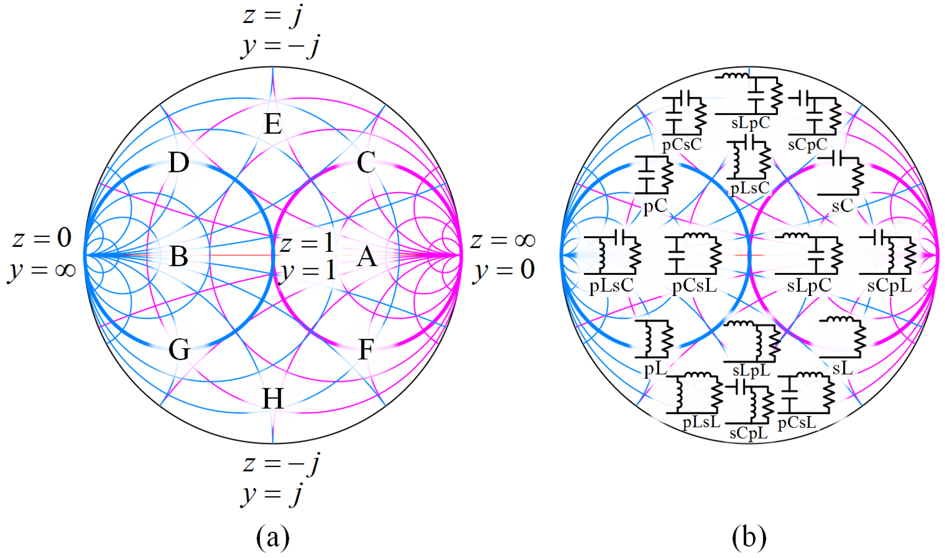
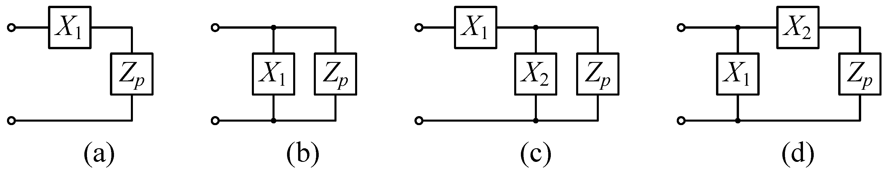
2.2. Simultaneous Conjugate Impedance Matching

To minimize unwanted electrical reflections at both ports of the acoustic-electric channel, electrical impedance matching networks are applied. The matching networks simultaneously conjugate match the impedance of the ports to 50 Ω , which is a widely used characteristic impedance value in RF systems. The theory of simultaneous conjugate matching was firstly presented by Rahola [23] and firstly adopted in a UTMWPT system by Lawry et al. [17] The matching networks were designed according to the scattering matrix (S-parameters) of the acoustic-electric channel. For ease of analysis, a simplified model of the impedance matched acoustic-electric channel is shown in Figure 3. Note that the RF PA together with the CW signal source is simplified to a voltage source with an output impedance, Z S , the RF AC-DC converter and load circuit are simplified to a resistor, Z L . In addition, Z S and Z L both equal 50 Ω .
The scattering matrix of the acoustic-electric channel, S , was measured using an AV36580A vector network analyzer (CETC41, Qingdao, Shandong, China). The TX transducer and RX transducer were connected to Port 1 and Port 2 of the network analyzer, respectively. The transducer power gain of the acoustic-electric channel, G T , is defined as the ratio of the power delivered to its load to the power available from its source. G T can be calculated as
G T = S 21 2
where S 21 is one of the four elements of S . The power transfer efficiency of the channel, η c h , is defined as a percentage and can be calculated directly from G T as
η c h = G T × 100 %
The impedance matrix of the channel, Z , can be derived from S as [24]
Z 11 = Z 0 1 + S 11 1 S 22 + S 12 S 21 1 S 11 1 S 22 S 12 S 21
Z 12 = Z 0 2 S 12 1 S 11 1 S 22 S 12 S 21
Z 21 = Z 0 2 S 21 1 S 11 1 S 22 S 12 S 21
Z 22 = Z 0 1 S 11 1 + S 22 + S 12 S 21 1 S 11 1 S 22 S 12 S 21
where Z 0 is the reference impedance of the network analyzer and it was set to 50 Ω . Then the simultaneously matched source and load impedances, Z m S and Z m L , can be calculated, respectively, by
Z m S = α 1 ± Δ 2 Re Z 22
Z m L = α 2 ± Δ 2 Re Z 11
where
α 1 = 2 j Re Z 22 Im Z 11 + j Im Z 12 Z 21
α 2 = 2 j Re Z 11 Im Z 22 + j Im Z 12 Z 21
Δ = 2 Re Z 11 Re Z 22 Re Z 12 Z 21 2 Z 12 Z 21 2
where the Re Z and Im Z notations represent the real and imaginary parts of a complex impedance Z. Care must be taken to select the appropriate signs of (7) and (8) to ensure that both Z m S and Z m L are positive. The impedances seen looking into Ports 1 and 2 under the conjugate matching condition, Z m 1 and Z m 2 , would simply be the complex conjugate of the matched source and load impedances, respectively, i.e.,
Z m 1 = Z m S *
Z m 2 = Z m L *
The scattering matrix of the simultaneously conjugate matched channel, S m , can be calculated by
S m = F Z Z m * Z + Z m 1 F 1
where
Z m = Z m S 0 0 Z m L
F = 2 Re Z m S 1 0 0 2 Re Z m L 1
The power transfer efficiency of the matched channel, η m c h , can be calculated by
η m c h = S m 21 2 × 100 %
where S m 21 is the element of S m . The matching networks will be designed at the frequency, denoted as f m c h , max , at which the maximum efficiency of the matched channel, η m c h , max , occurs.
Once Z m 1 and Z m 2 have been calculated at f m c h , max , impedance matching networks can be designed to transform each port impedance to the conjugate of a desired source or load impedance. The design method for each matching network is the same, so the following analysis focuses only on one channel port, the matched impedance of which is denoted simply as Z P . Figure 4 shows a Smith chart, which is normalized by the reference impedance Z 0 , and segmented into eight load regions (labelled A–H).
The port impedance of interest is likely to be complex such that Z P = R P + j X P . The normalized port impedance, z P = Z P / Z 0 , and the normalized port admittance, y P = z P 1 , can be plotted on the normalized Smith chart shown in Figure 4a. The normalized port impedance will fall into one of the eight regions on the Smith chart in Figure 4a. In each of these regions, a finite set of possible one-element or two-element matching networks exist that can be used to match the port and source impedances, as illustrated in Figure 4b. Table 1 lists the impedance range of and the network topologies available for each region. In the network topologies, `C’ and `L’ represent a capacitor and an inductor, respectively. Besides, `s’ represents that the reactance component after it, is connected in series with the channel port, while `p’ represents that the reactance component after it, is connected in parallel with the channel port. In two-element topologies, the second reactance component is close to the channel port. Figure 5 presents the set of fundamental one-element and two-element matching networks using component reactances X 1 and X 2 to generalize the specific L and C topologies.
For all one-element matching network topologies (sX and pX), the single reactance can be calculated by
X 1 = X P
For the sXpX topologies, the reactances can be calculated by
X 2 = Z 0 X P + a Z 0 R P R P 2 Z 0 R P + X P 2 Z 0 R P
X 1 = X 2 R P 2 + X 2 X P + X P 2 X 2 + X P 2 + R P 2
where a = 1 for the sLpL and sCpL configurations and a = 1 for the sLpC and sCpC configurations. For the pXsX topologies, the reactances can be calculated by
X 1 = b Z 0 R P Z 0 R P
X 2 = 1 2 X 1 X P 1 2 b X 1 2 4 R P 2
where b = 1 for the pLsL and pLsC configurations and b = 1 for the pCsL and pCsC configurations. Finally, the component types and sizes can be determined and calculated by
L = X n 2 π f m c h , max , if X n > 0 , n = 1 , 2 C = 1 2 π f m c h , max X n , if X n < 0 , n = 1 , 2
Figure 6 shows the power transfer efficiency of the unmatched channel, η c h , and the theoretical power transfer efficiency of the matched channel, η m c h , which are calculated from the channel’s scattering matrix, S . It can be seen from Figure 6 that the maximum efficiency of the unmatched channel is 33.1%, which occurs at 1157.2 kHz (denoted as f c h , max ). Under the conjugate matched condition, the channel’s maximum efficiency occurs at 945.0 kHz and increases to 56.0% (denoted as η m c h , max ). The curves of η c h and η m c h have a common periodicity. f c h , max = 1157 . 2 kHz differs greatly from f m c h , max = 945 . 0 kHz , the authors believe that it is mainly because the resonant frequencies of the commercial off-the-shelf transducers are not best matched with the thickness of the steel plate.
As f m c h , max has been determined, the matching networks are designed as Figure 7 shows. After applying the matching networks to the channel, the scattering matrix of the matched channel, S m , was measured using the vector network analyzer, in order to verify the effectiveness of the matching networks. The measured power transfer efficiency of the matched channel, η m c h , can be calculated from S m as
η m c h = S m 21 2 × 100 %
and is also plotted in Figure 6. The maximum value of η m c h , 41.7% (denoted as η m c h , max ), occurs at 944.6 kHz (denoted as f m c h , max ). The differences between η m c h , max and η m c h , max , f m c h , max and f m c h , max , are mainly caused by the non-ideality of the commercial off-the-shelf components, as well as the rounding error introduced when selecting available commercial off-the-shelf components. However, η m c h , max is still 8.6% than the peak value of η c h , therefore the matching networks is effective. In addition, η m c h , max is smaller than η m c h , max over the entire frequency band (excluding points near f m c h , max ), because η m c h , max was calculated at each frequency point while the matching networks were designed at the single point, f m c h , max .

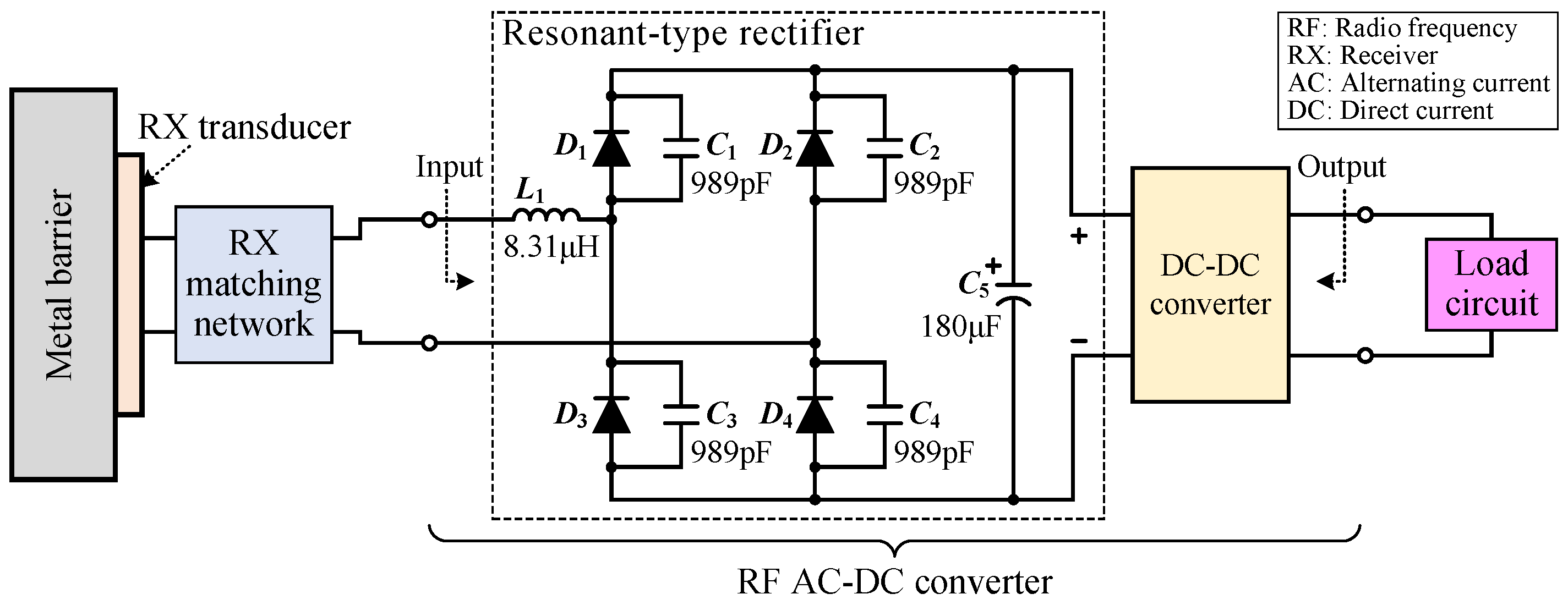
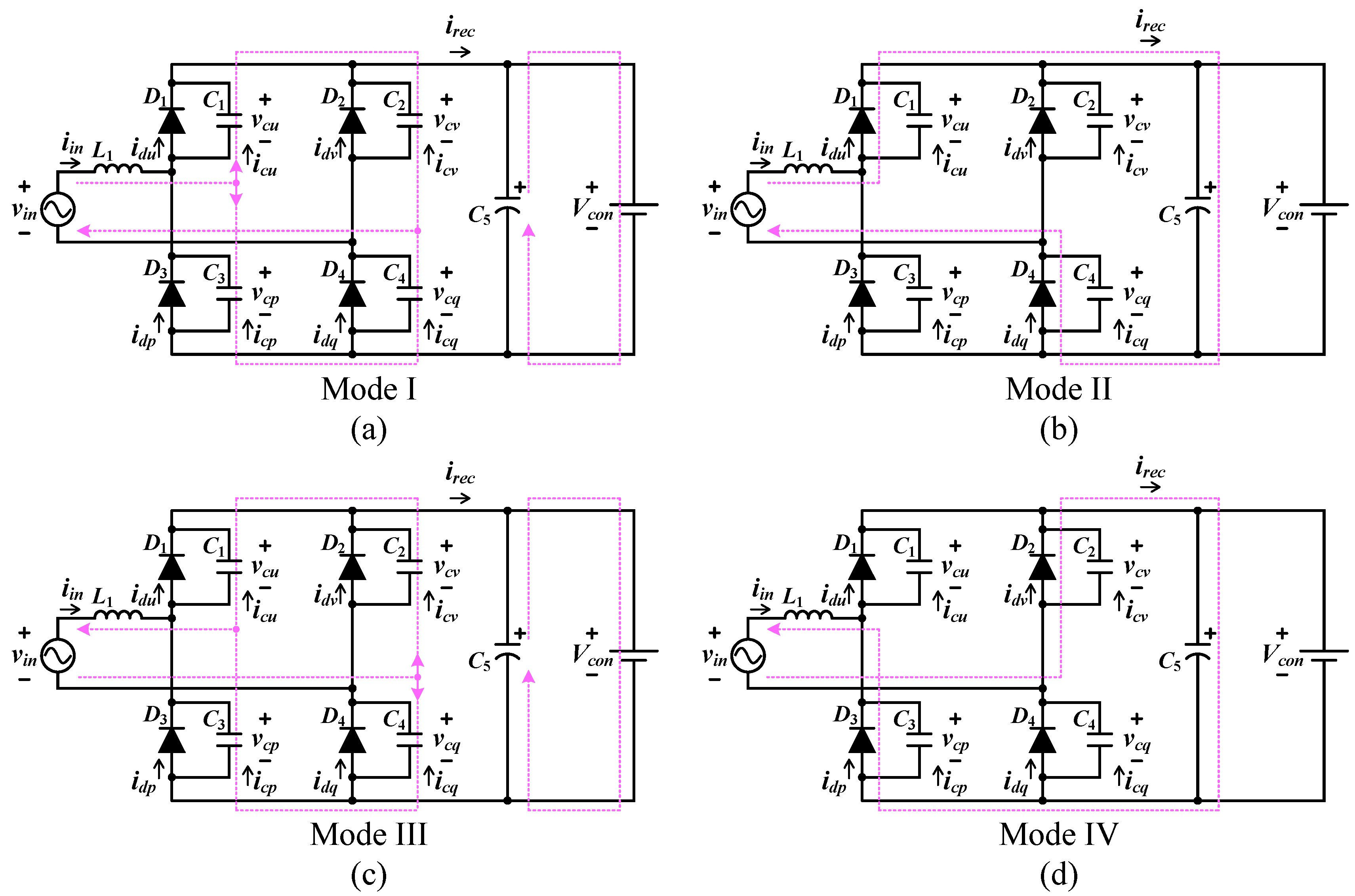
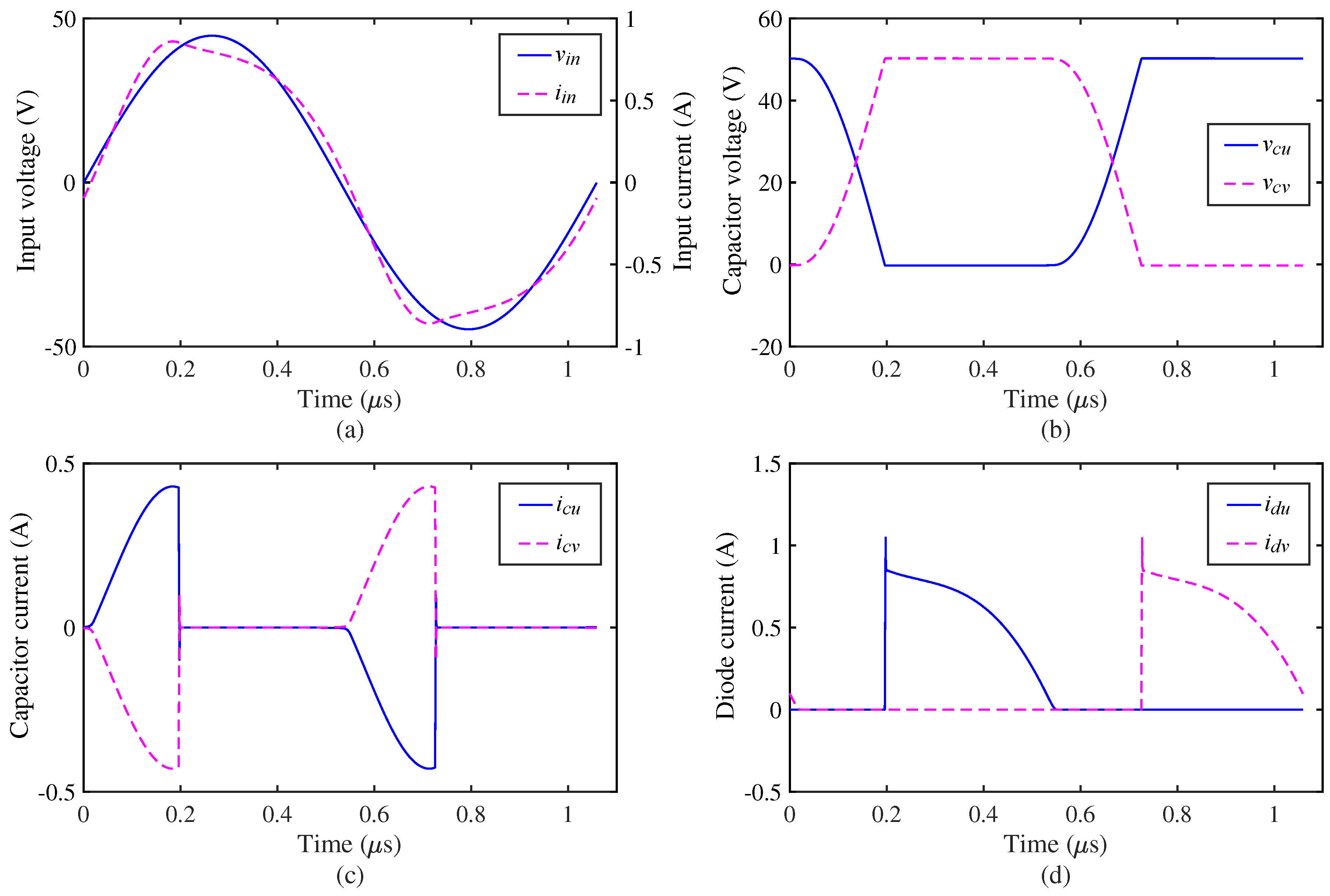
2.3. RF AC-DC Converter with Input Impedance Matching

The RF AC-DC converter with input impedance matching efficiently converts the RF output of the RX matching network to a regulated DC voltage. This is the main superiority of our UTMWPT system over previous ones. The RF AC-DC converter used in the system is constructed from a resonant-type rectifier and a DC-DC converter as shown in Figure 8. The resonant-type rectifier was originally proposed by Matsui et al. [25] as a high DC voltage generator. Kusaka et al. improved it and developed an AC-DC converter from it for a magnetic resonance coupling WPT system [26,27]. We simplified the topology proposed by Kusaka et al., and redesigned it for our UTMWPT system.
The resonant-type rectifier increases the conduction angle of the input current and the DC-DC converter stabilizes the operating point of the resonant-type rectifier [25,26,27]. These two features together achieve the input impedance matching of the AC-DC converter to the acoustic-electric channel. A resonant inductor L 1 and four resonant capacitors C 1 4 are added to the resonant-type rectifier as compared with conventional CF-DFBRs. As shown in Figure 9, one working period of the AC-DC converter can be divided into four modes according to the conduction states of the diodes. Note that the DC-DC converter is drawn as an ideal voltage source with voltage V c o n in Figure 9 because the DC-DC converter with large capacitance C 5 can be assumed as an ideal voltage source [26]. The operation modes of the AC-DC converter can be mathematically analyzed [25,26,27].
  • Operation Mode I
The input current starts to flow while the input voltage increases from zero. At the beginning of this mode, the initial current through the resonant inductor L 1 is assumed as zero, the resonant capacitors C 1 and C 4 have been charged during the Mode III in the previous working period. The voltages on C 1 and C 4 prevent the diodes D 1 and D 4 from turning on. Therefore, the input current flows through two paths: L 1 C 1 C 2 and L 1 C 3 C 4 . According to circuit theory, the input current i i n , I is derived as
i i n , I t = ω i n ω I 2 C V i n ω i n 2 ω I 2 cos ω I t cos ω i n t + ω I C V c o n sin ω I t
where ω i n is the angular frequency of the input voltage v i n , V i n is the amplitude of v i n , C = C 1 = C 2 = C 3 = C 4 is the resonant capacitance, and ω I is the resonant angular frequency in Mode I, which can be calculated by
ω I = 1 L 1 C
The resonant capacitors C 1 , C 4 and C 2 , C 3 are gradually discharged and charged, respectively, by the input current in Mode I. Once the capacitor voltages v c u , v c q decrease to zero and v c v , v c p increase to the voltage of voltage source, V c o n , the next operation mode starts. The duration of Mode I, T I , is equal to the discharging time of the capacitors C 1 , C 4 , and can be derived with numerical analytical approach from
V c o n 2 1 + cos ω I T I + ω I V i n 2 ω i n 2 ω I 2 ω I sin ω i n T I ω i n sin ω I T I = 0
  • Operation Mode II
As the capacitor voltages v c u and v c q decrease to zero, the diodes D 1 and D 4 turn on. The path of the input current changes to L 1 D 1 C 5 D 4 . The input current charges the smoothing capacitor C 5 and can be calculated by
i i n , II t = i i n , I T I · cos ω II t T I V c o n ω II L 1 sin ω II t T I + V i n cos ω i n T I ω i n 2 ω II 2 L 1 ω i n cos ω II t T I ω i n cos ω i n t T I + V i n sin ω i n T I ω i n 2 ω II 2 L 1 ω i n sin ω i n t T I ω II sin ω II t T I
where ω II is the resonant angular frequency in Mode II and can be calculated by
ω II = 1 L 1 C 5
Because the smoothing capacitance C 5 is large, ω II can be ignored. Then (28) is simplified to
i i n , II t i i n , I T I V c o n L 1 t T I + V i n ω i n L 1 cos ω i n T I cos ω i n t
In addition, the capacitor voltages v c u , v c v , v c p and v c q all remain unchanged in this mode. Mode II ends when the polarity of the input voltage changes from positive to negative.
  • Operation Mode III
In this mode, the input current flows in two paths: C 2 C 1 L 1 and C 4 C 3 L 1 , which are the opposite directions to those in Mode I. The input current in Mode III is expressed by
i i n , III t = i i n , I t T 2
where T is the period of the input voltage. The capacitors C 2 , C 3 and C 1 , C 4 are gradually discharged and charged, respectively, by the input current.
Once the capacitor voltages v c v , v c p decrease to zero and v c u , v c q increase to V c o n , the next operation mode starts. The duration of Mode III is the same to that of Mode I.
  • Operation Mode IV
As the capacitor voltages v c v and v c p decrease to zero, the diodes D 2 and D 3 turn on. The path of the input current changes to D 2 C 5 D 3 L 1 . The input current in Mode IV is expressed by
i i n , IV t = i i n , II t T 2
Mode IV ends when the polarity of the input voltage changes from negative to positive. Then the Mode I of the next working period starts.
According to (25) and (30), the amplitude and phase of the input current are determined by the resonant parameters: the capacitance C, inductance L 1 , the relation between the input voltage amplitude V i n and rectifier output voltage V c o n . Therefore, the intended input impedance of the AC-DC converter, which is the same as the output impedance of the matched acoustic-electric channel, can be obtained by designing these parameters properly. The design procedure contains eight steps as follows [26].
  • Step 1: Derivation of the input voltage amplitude V i n
Because the input impedance of the AC-DC converter is to be matched to the output impedance of the matched acoustic-electric channel, which is 50 Ω , the input current of the AC-DC converter will be in-phase with the input voltage. The amplitude of the input voltage, V i n , can be calculated by
V i n = 2 P i n Re Z i n , A C D C
where Z i n , A C D C = 50 + j 0 Ω is the intended input impedance of the AC-DC converter, and P i n is the input power of the AC-DC converter.
  • Step 2: Decision of the resonant-type rectifier output voltage V c o n
When deciding the output voltage of the resonant-type rectifier, V c o n , two requirements should be met. One is that V c o n must be within the rated input voltage range of the DC-DC converter. The other is that V c o n must be higher than V i n , because the resonant-type rectifier is a kind of step-up converter [25].
  • Step 3: Calculation of the voltage ratio α V
The voltage ratio α V is defined as
α V = V c o n V i n
As mentioned above, the relation between V i n and V c o n is one of the resonant parameters. α V would be remained constant through the operation of the AC-DC converter.
  • Step 4: Derivation of the frequency ratio α f
The frequency ratio α f is defined as
α f = f r e f i n
where f i n = ω i n / 2 π is the frequency of the input voltage, and
f r e = 1 2 π L 1 C / 2
is the resonant frequency of the rectifier.
α f can be derived from numerical analysis based on circuit simulation as
α f 1 . 680 α V 3 + 9 . 045 α V 2 16 . 616 α V + 12 . 248
  • Step 5: Derivation of a non-dimensional parameter β
β is a non-dimensional parameter defined as
β = Re Z i n , A C D C 2 π f i n L 1
β needs also to be derived from numerical analysis based on circuit simulation. The approximation formula is expressed by
β 0 . 642 α V 3 + 3 . 630 α V 2 7 . 132 α V + 5 . 348
  • Step 6: Calculation of the resonant inductance L 1
Once β is calculated, the resonant inductance L 1 can be calculated from (38).
  • Step 7: Calculation of the resonant frequency f r e
The resonant frequency f r e can be get by substituting the calculated α f into (35).
  • Step 8: Calculation of the resonant capacitance C
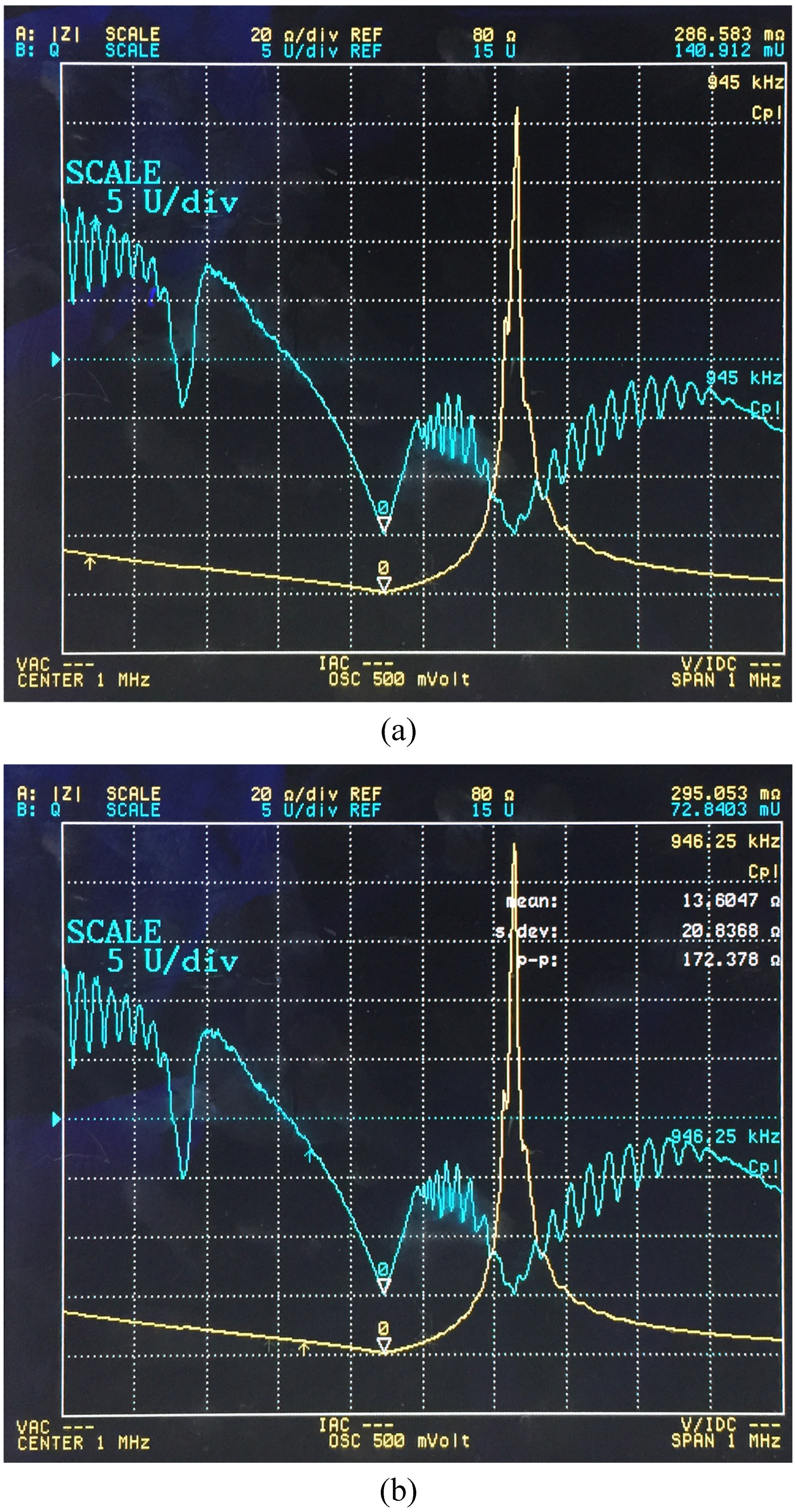
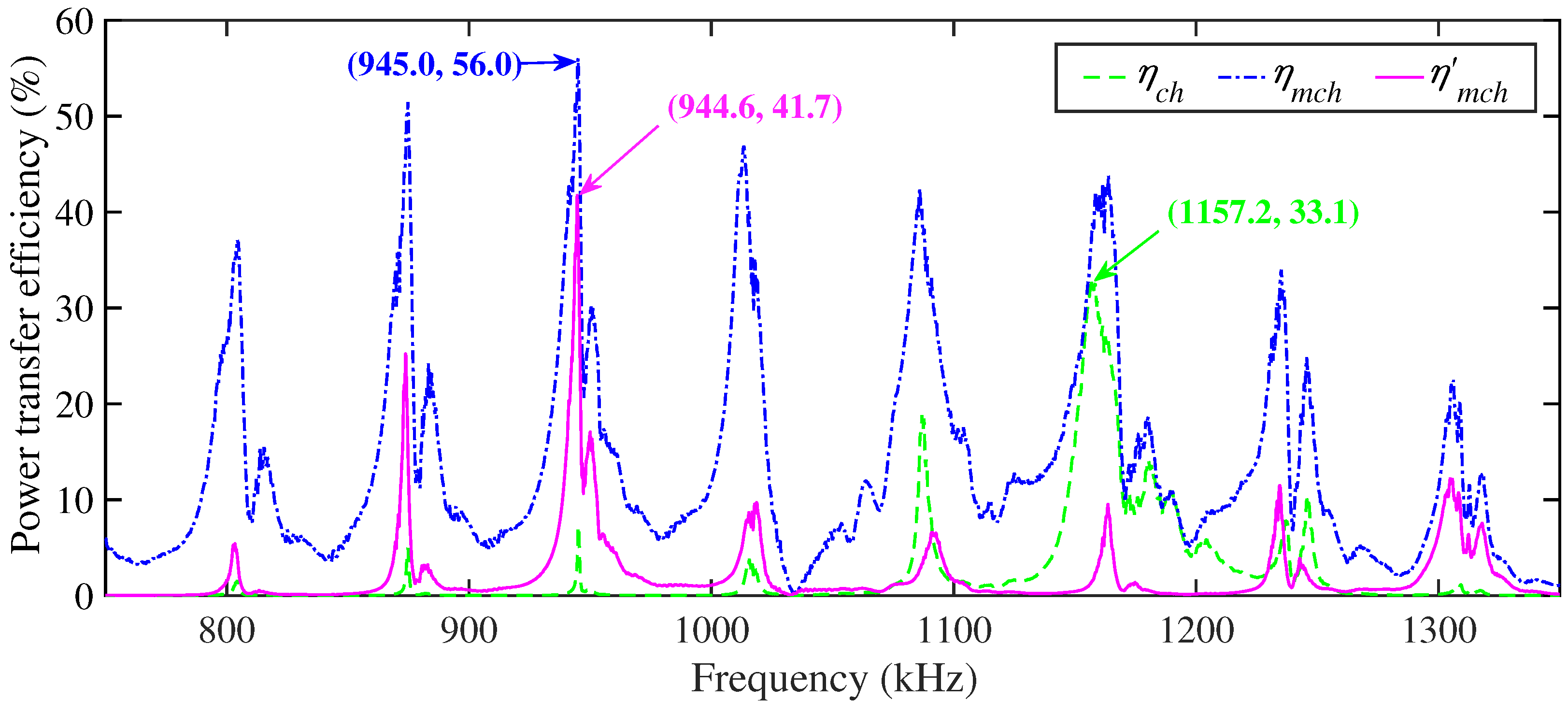
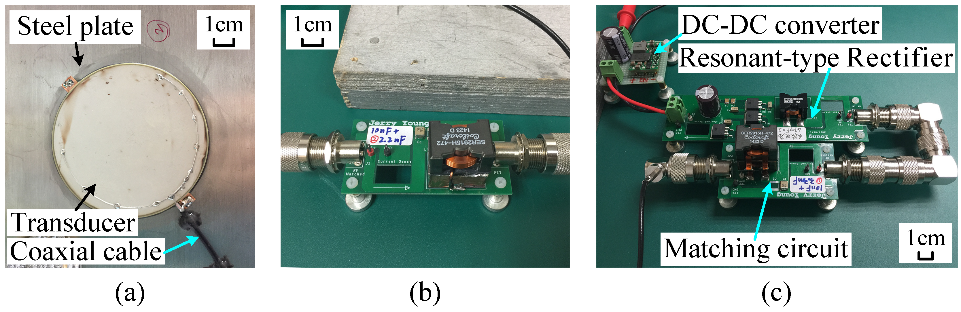
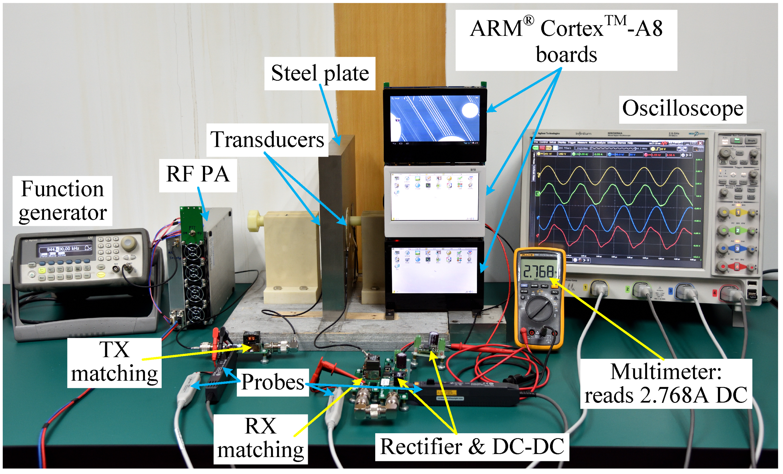
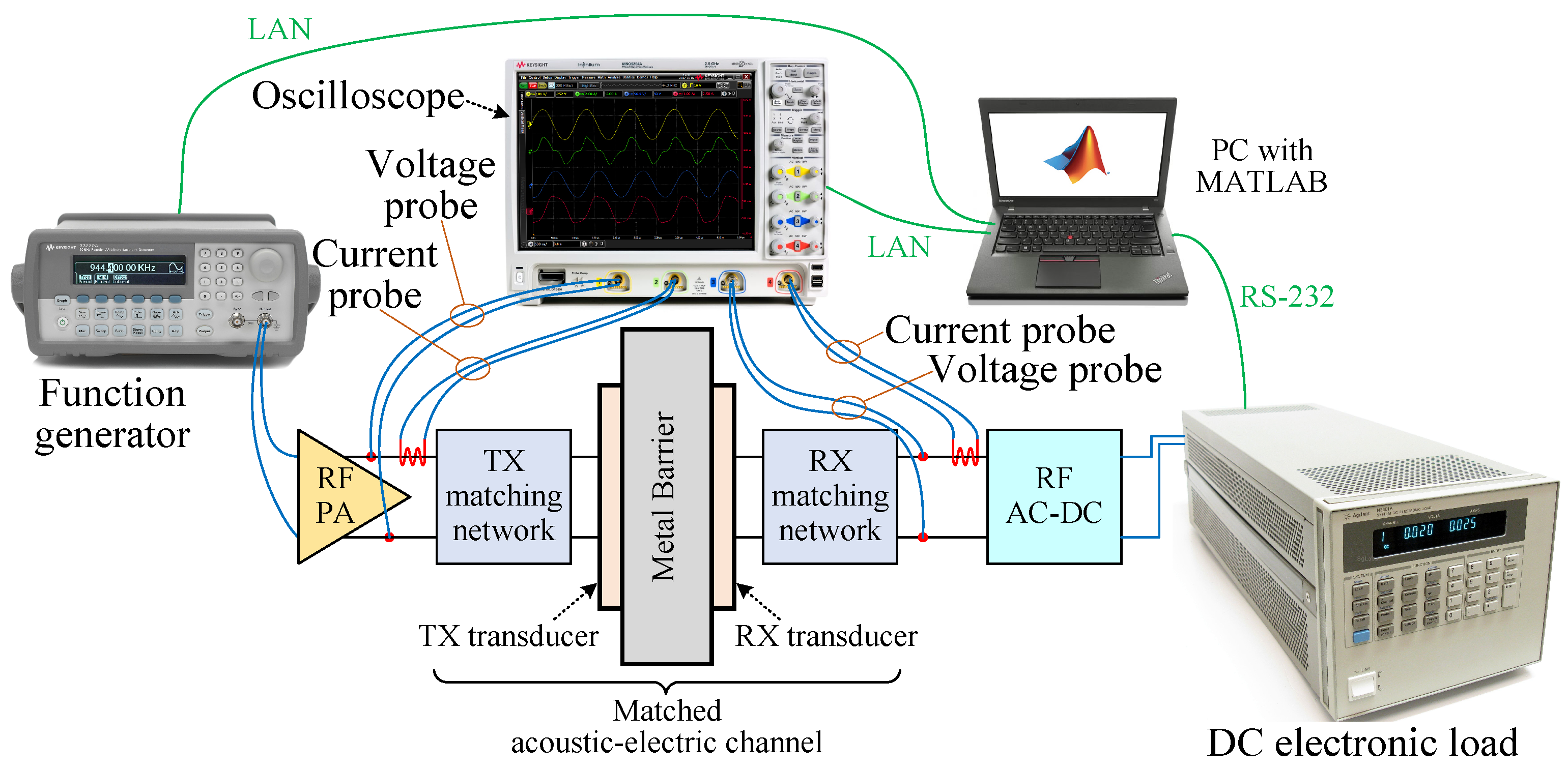
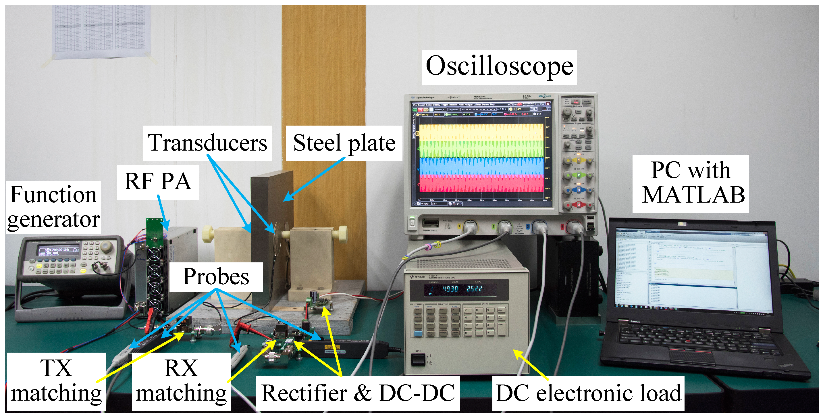
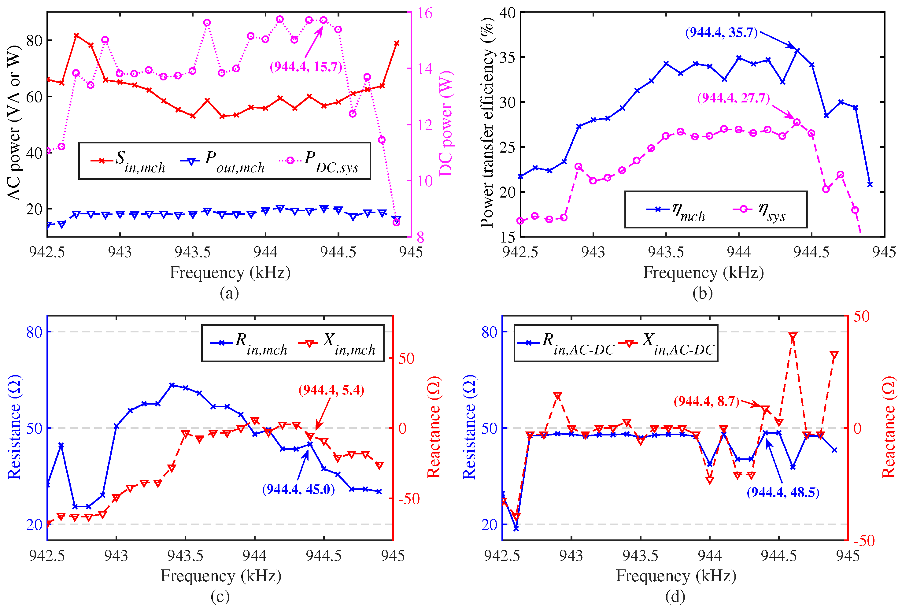
The resonant capacitance C can be get by substituting the calculated L 1 and f r e into (36).
The resonant parameters of the AC-DC converter used in the system were determined according to the steps above. Table 2 lists all the parameters of the AC-DC converter. These parameters were confirmed by a PSpice (Cadence Design Systems Inc., San Jose, CA, USA) simulation. Figure 10 shows the simulation waveforms in one period of the input voltage.
A commercial PKB4713PINB 5-V output isolated step-down DC-DC module (Ericsson AB, Stockholm, Sweden) is used as the DC-DC converter in the system. The use of a commercial off-the-shelf module instead of a custom designed converter allows a fast and stable system implementation. The circuits and one of the transducers of the system are shown in Figure 11. The component values in Table 1, as well as those in Figure 3, were rounded to find appropriate commercial off-the-shelf components. The inductors are from Coil-Craft Inc. (Cary, IL, USA) and Würth Elektronik GmbH & Co. KG (Niedernhall, Germany). The capacitors are from Murata Manufacturing Co., Ltd (Nagaokakyo-shi, Kyoto, Japan). The diodes are silicon carbide (SiC) Schottky barrier diodes from Cree Inc. (Durham, NC, USA).

3. Measurements

To verify the operation of the full system, the output power, power transfer efficiency, and port impedances were measured. The measurement configuration is shown in Figure 12. A Keysight 33220A function generator was used as the CW signal source. It was set to the continuous sine wave output mode. The measurements were carried out using a Keysight MSO9254A oscilloscope by connecting Keysight N2904A differential voltage probes and Keysight 1147B current probes to the input port and output port of the matched acoustic-electric channel. To measure the exact power output capacity of the system, a Keysight N3301A DC electronic load was used. It was set to the constant voltage mode. The function generator, oscilloscope and DC electronic load were all automatically controlled by a MATLAB (MathWorks Inc., Natick, MA) script on a personal computer (PC) to guarantee their synchronization. The fully automated measurements are faster, more objective and more precise than previous methods [15,16,17,18]. This is because the entire process does not require manual intervention and all measurement results are automatically read by the MATLAB script. Furthermore, the impedance mismatch caused by the error of the circuits, which was ignored in [15,16,17,18], was taken into account during the measurements. A photo of the measurement setup is presented in Figure 13.
The output frequency of the function generator was scanned from 942.5 kHz to 944.9 kHz to find the most efficient working frequency of the system. Furthermore, at each frequency, the minimum output amplitude of the function generator, ensuring that the AC-DC converter operated stably, was determined using the bisection method. The automated measurement algorithm is given in Algorithm 1. Note that before carrying out the measurements, the time delay between the current and voltage probes has to be calibrated by using a Keysight U1880A deskew fixture. In order to make accurate measurements based on the voltage across and current through fast switching devices, it is  important that any skew between the voltage probe and current probe signal paths is corrected [28]. After finishing the measurements, the parameters characterizing performance of the system can be either directly known or indirectly calculated from the data recorded during the measurements. These parameters are plotted in Figure 14.
Algorithm 1 Automated measurement algorithm of the system.
1:
Initialization: Connect the instruments and load basic settings;
2:
f F G _ N E X T 942 . 5 kHz ;
3:
Set output frequency of 33220A f F G f F G _ N E X T ; V F G _ N E X T 170 m V pp ;
4:
REG _ Flag F a l s e ; V F G _ R E G _ M I N 0 ; V F G _ u n R E G _ M A X 0 ;
5:
Set output amplitude of 33220A V F G V F G _ N E X T ;
6:
Enable output of 33220A; Trigger N3301A and wait for 20 seconds;
7:
if N3301A is in an unregulated state then
8:
    Disable output of 33220A;
9:
    if V F G = 170 m V pp or REG _ Flag = F a l s e and V F G _ R E G _ M I N = 0 then
10:
         V F G _ u n R E G _ M A X V F G ; V F G _ N E X T V F G + 5 m V p p ;
11:
    else if REG _ Flag = F a l s e and V F G _ R E G _ M I N 0 then
12:
        if V F G > V F G _ u n R E G _ M A X then V F G _ u n R E G _ M A X V F G ;
13:
         V F G _ N E X T ceil V F G _ u n R E G _ M A X + V F G _ R E G _ M I N ÷ 2 ;
14:
    else if REG _ Flag = T r u e and V F G _ u n R E G _ M A X = 0 then
15:
         V F G _ u n R E G _ M A X V F G ; V F G _ N E X T ceil V F G + V F G _ R E G _ M I N ÷ 2 ;
16:
    else if REG _ Flag = T r u e and V F G _ u n R E G _ M A X 0 then
17:
        if V F G < V F G _ R E G _ M I N then V F G _ R E G _ M I N V F G ;
18:
         V F G _ N E X T ceil V F G _ u n R E G _ M A X + V F G _ R E G _ M I N ÷ 2 ;
19:
     REG _ Flag F a l s e ;
20:
else
21:
    Wait until MSO9254A and N3301A finish acquisition and measurements;
22:
    Disable output of 33220A and save acquired waveform data and measurement results;
23:
    if V F G = 170 m V pp or REG _ Flag = T r u e and V F G _ u n R E G _ M A X = 0 then
24:
         V F G _ R E G _ M I N V F G ; V F G _ N E X T V F G 5 m V p p ;
25:
    else if REG _ Flag = T r u e and V F G _ u n R E G _ M A X 0 then
26:
        if V F G < V F G _ R E G _ M I N then V F G _ R E G _ M I N V F G ;
27:
         V F G _ N E X T ceil V F G _ u n R E G _ M A X + V F G _ R E G _ M I N ÷ 2 ;
28:
    else if REG _ Flag = F a l s e and V F G _ R E G _ M I N = 0 then
29:
         V F G _ R E G _ M I N V F G ; V F G _ N E X T ceil V F G _ u n R E G _ M A X + V F G ÷ 2 ;
30:
    else if REG _ Flag = F a l s e and V F G _ R E G _ M I N 0 then
31:
        if V F G < V F G _ R E G _ M I N then V F G _ R E G _ M I N V F G ;
32:
         V F G _ N E X T ceil V F G _ u n R E G _ M A X + V F G _ R E G _ M I N ÷ 2 ;
33:
     REG _ Flag T r u e ;
34:
if V F G _ N E X T 210 m V pp and V F G _ N E X T V F G then goto 5;
35:
if f F G < 944 . 9 kHz then f F G _ N E X T f F G + 0 . 1 kHz ; goto 3;
36:
Finish: Disconnect the instruments;
Figure 14a,b show that the highest DC output power (15.7 W) and the maximum power transfer efficiency of the system (27.7%) both occur at 944.4 kHz. The power transfer efficiency of the system is defined as
η s y s = P D C , s y s S i n , m c h × 100 %
where S i n , m c h is the input apparent power of the matched channel. The apparent power was calculated from the product of the root-mean-square values of the voltage and current [29]. The power transfer efficiency of the matched acoustic-electric channel was calculated by
η m c h = P o u t , m c h S i n , m c h × 100 %
where P o u t , m c h is the output active power of the matched channel. P o u t , m c h was calculated by
P o u t , m c h = 1 T m e a s 0 T m e a s v o u t , m c h t i o u t , m c h t d t
where v o u t , m c h t and i o u t , m c h t are the transient output voltage and current of the matched channel, respectively, T m e a s is the measurement time [29].
Figure 14c shows the input resistance and reactance of the matched channel while Figure 14d shows those of the AC-DC converter. The input resistance of the matched channel was calculated by
R i n , m c h = U i n 1 st , m c h I i n 1 st , m c h × cos θ i n 1 st , m c h
where U i n 1 st , m c h is the root-mean-square value of the fundamental-frequency component of the matched channel’s input voltage, I i n 1 st , m c h is the root-mean-square value of the fundamental-frequency component of the matched channel’s input current, and θ i n 1 st , m c h is the phase angle difference between I i n 1 st , m c h and U i n 1 st , m c h . The input reactance of the matched channel was calculated by
X i n , m c h = U i n 1 st , m c h I i n 1 st , m c h × sin θ i n 1 st , m c h
Similarly, the AC-DC converter’s input resistance R i n , A C D C and input reactance X i n , A C D C was calculated by
R i n , A C D C = U i n 1 st , A C D C I i n 1 st , A C D C × cos θ i n 1 st , A C D C
and
X i n , A C D C = U i n 1 st , A C D C I i n 1 st , A C D C × sin θ i n 1 st , A C D C
respectively. The values of R i n , m c h , X i n , m c h , R i n , A C D C and X i n , A C D C at the system’s most efficient point (944.4 kHz) can be read from Figure 14c,d. Then the values of the input impedances of the match channel and the AC-DC converter at the system’s most efficient point can be calculated as
Z i n , m c h = R i n , m c h + j X i n , m c h = 45 . 0 + 5 . 4 j Ω = 45 . 3 Ω 21 . 5
and
Z i n , A C D C = R i n , A C D C + j X i n , A C D C = 48 . 5 + 8 . 7 j Ω = 49 . 3 Ω 32 . 0
respectively. From these values, it can be concluded that both the channel and the AC-DC converter were matched relatively well.
As mentioned in Section 1, Bao et al., did not apply any AC-DC conversion circuit in their UTMWPT systems [15,16]. Systems presented by Leung et al. could at best output only about 1.0 W of AC power [21]. Hu et al. greatly simplified the UTMWPT system model in simulation and did not present experimental results [14]. Only Lawry et al. presented a medium-power DC output UTMWPT system, as well as experimental results [17,18]. Table 3 shows a comparison between our system and the system presented by Lawry et al. The maximum power transfer efficiency of the acoustic-electric channel in Lawry’s system is 51%, which is 15.3% higher than that of our system. We believe that this is due primarily to two factors. First, the performance of the commercial off-the-shelf transducers we used is lower than that of the custom-designed transducers used by Lawry. Second, as mentioned in Section 2.2, the resonant frequencies of the transducers are not best matched with the thickness of the steel plate in our system [17]. These two problems can both be solved by custom designing new low-loss transducers.
However, in spite of the disadvantages, the maximum DC output efficiency of our system (27.7%) is still 8.7% higher than that of Lawry’s system (19%), while the maximum DC output power of our system (15.7 W) is commensurate with that of Lawry’s system (19 W). Furthermore, the output voltage of Lawry’s system is not regulated, which greatly limits its usefulness. Therefore, the UTMWPT system which we present in this paper is superior to previous ones. More importantly, the effectiveness of this system has been successfully demonstrated using three ARM® Cortex™-A8 evaluation boards with LCD panels, as shown in Figure 15. The ARM® boards are used as the load circuit in Figure 1, and the power input ports of them are connected in parallel. The peak total power consumption of the ARM® boards when loading operating systems is about 17 W. After booting up, the dynamic power consumption of the boards fluctuates between 13 W and 17 W. The demonstration experiment lasted for an hour, the circuits and the transducers did not overheat and the ARM® boards worked continuously and stably during the experiment. Therefore, this system can certainly be applied to almost all medium-power electronic/electric appliances.

4. Conclusions

A novel UTMWPT system has been presented that is capable of transmitting electric energy through a 40-mm-thick stainless steel plate and output 15.7 W of DC power regulated at 5 V with an overall efficiency of up to 27.7%. An RF AC-DC converter with input impedance matching is used in this system to achieve the high RF AC to DC conversion efficiency. The performance of the full system was tested using a computer-controlled measurement method, which has been presented as well. The practical effectiveness of the system has also been successfully demonstrated using ARM® Cortex™-A8 evaluation boards with LCD panels. In addition, the authors believe that higher power transfer efficiency and higher output power could be achieved with the use of custom-designed transducers, inductors and capacitors, as well as a more powerful PA. This system can be applied in many industrial and military applications to power sensors and electronic circuits operating inside or outside hermetic metal containers, such as submarines, space crafts, planes and nuclear storage facilities, etc., for increased safety and reduced maintenance costs.

Author Contributions

The author gratefully acknowledges the co-authors for their support and contribution to this work. H.Y. conceived the work and undertook the experiments. J.Y. and M.W. are his thesis supervisors and provided critical comments and guidance for the work. Z.Y. provided funding and facilities support for the experiment. All the authors have given final approval of the version to be published.

Acknowledgments

This work was supported by the IACAS Young Elite Researcher Project QNYC201722 and the National Natural Science Fund of China under Grant 11472307.

Conflicts of Interest

The authors declare no conflict of interest.

References

  1. Kurs, A.; Karalis, A.; Moffatt, R.; Joannopoulos, J.D.; Fisher, P.; Soljacic, M. Wireless Power Transfer via Strongly Coupled Magnetic Resonances. Science 2007, 317, 83–986. [Google Scholar] [CrossRef] [PubMed]
  2. Moradewicz, A.J.; Kazmierkowski, M.P. Contactless Energy Transfer System With FPGA-Controlled Resonant Converter. IEEE Trans. Ind. Electron. 2010, 57, 3181–3190. [Google Scholar] [CrossRef]
  3. Hu, Y.; Zhang, X.; Yang, J.; Jiang, Q. Transmitting electric energy through a metal wall by acoustic waves using piezoelectric transducers. IEEE Trans. Ultrason. Ferroelectr. Freq. Control 2003, 50, 773–781. [Google Scholar] [CrossRef] [PubMed]
  4. Yang, D.X.; Hu, Z.; Zhao, H.; Hu, H.F.; Sun, Y.Z.; Hou, B.J. Through-Metal-Wall Power Delivery and Data Transmission for Enclosed Sensors: A Review. Sensors 2015, 15, 31581–31605. [Google Scholar] [CrossRef] [PubMed]
  5. Zhang, J.; Yu, Z.; Yang, H.; Wu, M.; Yang, J. In Wireless communication using ultrasound through metal barriers: Experiment and analysis. In Proceedings of the 2015 10th International Conference on Information, Communications and Signal Processing (ICICS), Singapore, 2–4 December 2015. [Google Scholar]
  6. Cotte, B.; Lafon, C.; Dehollain, C.; Chapelon, J.Y. Theoretical study for safe and efficient energy transfer to deeply implanted devices using ultrasound. IEEE Trans. Ultrason. Ferroelectr. Freq. Control 2012, 59, 1674–1685. [Google Scholar] [CrossRef] [PubMed]
  7. Denisov, A.; Yeatman, E. Ultrasonic vs. Inductive power delivery for miniature biomedical implants. In Proceedings of the 2010 International Conference on Body Sensor Networks, Singapore, 7–9 June 2010. [Google Scholar]
  8. Guida, R.; Santagati, G.E.; Melodia, T. A 700 khz ultrasonic link for wireless powering of implantable medical devices. In Proceedings of the 2016 IEEE SENSORS, Orlando, FL, USA, 30 October–3 November 2016. [Google Scholar]
  9. Basaeri, H.; Christensen, D.; Roundy, S.; Yu, Y.; Nguyen, T.; Tathireddy, P.; Young, D.J. Ultrasonically powered hydrogel-based wireless implantable glucose sensor. In Proceedings of the 2016 IEEE SENSORS, Orlando, FL, USA, 30 October–3 November 2016. [Google Scholar]
  10. Lin, Y.C.; Chiang, M.C.; Chen, J.H. A wireless sensor utilizing ultrasound for wireless power and data transmission. In Proceedings of the 2017 IEEE Wireless Power Transfer Conference (WPTC), Taipei, Taiwan, 10–12 May 2017. [Google Scholar]
  11. Tseng, V.F.G.; Bedair, S.S.; Lazarus, N. Acoustic wireless power transfer with receiver array for enhanced performance. In Proceedings of the 2017 IEEE Wireless Power Transfer Conference (WPTC), Taipei, Taiwan, 10–12 May 2017. [Google Scholar]
  12. Du, G.; Zhu, Z.; Gong, X. Fundamentals of Acoustics, 3rd ed.; Nanjing University Press: Nanjing, China, 2012; pp. 351–352. ISBN 9787305097782. [Google Scholar]
  13. International Telecommunication Union (ITU). Nomenclature of the Frequency and Wavelength Bands Used in Telecommunications; International Telecommunication Union (ITU): Geneva, Switzerlandm, 1865; Available online: https://www.itu.int/dms_pubrec/itu-r/rec/v/R-REC-V.431-7-200005-S!!PDF-E.pdf (accessed on 4 March 2018).
  14. Hu, H.; Hu, Y.; Chen, C.; Wang, J. A system of two piezoelectric transducers and a storage circuit for wireless energy transmission through a thin metal wall. IEEE Trans. Ultrason. Ferroelectr. Freq. Control 2008, 55, 2312–2319. [Google Scholar] [CrossRef] [PubMed]
  15. Bao, X.Q.; Doty, B.J.; Sherrit, S.; Badescu, M.; Cohen, Y.B.; Aldrich, J.; Chang, Z.S. Wireless piezoelectric acoustic-electric power feedthru. In Proceedings of the Sensors and Smart Structures Technologies for Civil, Mechanical, and Aerospace Systems 2007, San Diego, CA, USA, 19–22 March 2007; Tomizuka, M., Yun, C.-B., Giurgiutiu, V., Eds.; SPIE: Bellingham, WA, USA, 2007. [Google Scholar]
  16. Bao, X.Q.; Biederman, W.; Sherrit, S.; Badescu, M.; Cohen, Y.B.; Jones, C.; Aldrich, J.; Chang, Z.S. High-power piezoelectric acoustic-electric power feedthru for metal walls. In Proceedings of the Industrial and Commercial Applications of Smart Structures Technologies 2008, San Diego, CA, USA, 10–12 March 2008; Porter Davis, L., Henderson, B.K., Brett McMickell, M., Eds.; SPIE: Bellingham, WA, USA, 2007. [Google Scholar]
  17. Lawry, T.J. A High Performance System for Wireless Transmission of Power and Data through Solid Metal Enclosures. Ph.D. Thesis, Rensselaer Polytechnic Institute, Troy, NY, USA, 2011. [Google Scholar]
  18. Lawry, T.J.; Wilt, K.R.; Ashdown, J.D.; Scarton, H.A.; Saulnier, G.J. A high-performance ultrasonic system for the simultaneous transmission of data and power through solid metal barriers. IEEE Trans. Ultrason. Ferroelectr. Freq. Control 2013, 60, 194–203. [Google Scholar] [CrossRef] [PubMed]
  19. Leung, H.F.; Hu, A.P. Theoretical modeling and analysis of a wireless ultrasonic power transfer system. In Proceedings of the 2015 IEEE PELS Workshop on Emerging Technologies: Wireless Power (2015 WoW), Daejeon, Korea, 5–6 June 2015. [Google Scholar]
  20. Dai, X.; Li, L.; Li, Y.; Hou, G.; Leung, H.F.; Hu, A.P. Determining the maximum power transfer condition for ultrasonic power transfer system. In Proceedings of the 2016 IEEE 2nd Annual Southern Power Electronics Conference (SPEC), Auckland, New Zealand, 5–8 December 2016. [Google Scholar]
  21. Rezaie, H.; Hu, A.P.; Leung, H.F.; Cordell, R. New attachment method to increase the performance of ultrasonic wireless power transfer system. In Proceedings of the 2017 IEEE PELS Workshop on Emerging Technologies: Wireless Power Transfer (WoW), Chongqing, China, 20–22 May 2017. [Google Scholar]
  22. Feng, R.; Yao, J.; Guan, L. Ultrasonics Handbook; Nanjing University Press: Nanjing, China, 1999; pp. 233–234. ISBN 9787305033544. [Google Scholar]
  23. Rahola, J. Power waves and conjugate matching. IEEE Trans. Circuits Syst. II Exp. Briefs 2008, 55, 92–96. [Google Scholar] [CrossRef]
  24. Pozar, D.M. Microwave Engineering, 4th ed.; John Wiley & Sons, Inc.: Hoboken, NJ, USA, 2011; pp. 165–192. ISBN 9781118298138. [Google Scholar]
  25. Matsui, K.; Yamamoto, I.; Guan, E.; Hasegawa, M.; Ando, K.; Ueda, F.; Mori, H. A High DC voltage Generator by LC Resonance in Commercial Frequency. In Proceedings of the 2007 Power Conversion Conference, Nagoya, Janpan, 2 April 2007. [Google Scholar]
  26. Kusaka, K.; Itoh, J.I. Experimental verifications and desing procedure of an AC-DC converter with input impedance matching for wireless power transfer systems. In Proceedings of the 2013 IEEE Energy Conversion Congress and Exposition, Denver, CO, USA, 15 September 2013. [Google Scholar]
  27. Kusaka, K.; Itoh, J.I. Input impedance matched AC-DC converter in wireless power transfer for EV charger. In Proceedings of the 2012 15th International Conference on Electrical Machines and Systems (ICEMS), Sapporo, Japan, 21–24 October 2012. [Google Scholar]
  28. Keysight Technologies, Inc. Keysight U1880A Deskew Fixture User’s Guide; Keysight Technologies, Inc.: Santa Rosa, CA, USA, 2014; Available online: https://literature.cdn.keysight.com/litweb/pdf/U1880-97000.pdf (accessed on 10 February 2018).
  29. Qiu, G.Y.; Luo, X.J. Circuit, 5th ed.; Higher Education Press: Beijing, China, 2006; pp. 233–238. ISBN 9787040196719. [Google Scholar]
Figure 1. Block diagram of the ultrasonic through-metal-wall power transfer system.
Applsci 08 00692 g001
Figure 2. Impedance and quality factor measurement results of the transducers (frequency range: 0.5–1.5 MHz): (a) Impedance modulus (yellow) and quality factor (cyan) of the TX (transmitter) transducer; (b) Impedance modulus (yellow) and quality factor (cyan) of the RX (receiver) transducer.
Applsci 08 00692 g002
Figure 3. Simplified model of the impedance matched acoustic-electric channel.
Applsci 08 00692 g003
Figure 4. Normalized smith chart for matching network design: (a) Load regions; (b) Matching network topologies.
Applsci 08 00692 g004
Figure 5. Fundamental matching Network Topologies: (a) sX; (b) pX; (c) sXpX; (d) pXsX.
Applsci 08 00692 g005
Figure 6. Power transfer efficiencies of the unmatched and matched channel.
Applsci 08 00692 g006
Figure 7. Matching network topology and component values: (a) TX matching network; (b) RX matching network.
Applsci 08 00692 g007
Figure 8. Schematic of the RF AC-DC converter used in the system.
Applsci 08 00692 g008
Figure 9. Operation modes of the AC-DC converter: (a) Mode I; (b) Mode II; (c) Mode III; (d) Mode IV.
Applsci 08 00692 g009
Figure 10. PSpice simulation waveforms of the AC-DC converter used in the system: (a) Waveforms of the input voltage and input current; (b) Waveforms of the voltages across C 1 and C 2 ; (c) Waveforms of the currents through C 1 and C 2 ; (d) Waveforms of the currents through D 1 and D 2 .
Applsci 08 00692 g010
Figure 11. (a) One of the transducers; (b) TX matching circuit; (c) RX matching circuit and AC-DC converter.
Applsci 08 00692 g011
Figure 12. System measurement configuration.
Applsci 08 00692 g012
Figure 13. Photo of the system measurement setup.
Applsci 08 00692 g013
Figure 14. Measurement results of the system: (a) Input apparent power and output active power of the matched channel and DC output power of the system; (b) Power transfer efficiency of the matched channel and system; (c) Input resistance and reactance of the matched channel; (d) Input resistance and reactance of the AC-DC converter.
Applsci 08 00692 g014
Figure 15. Practical setup of the UTMWPT system.
Applsci 08 00692 g015
Table 1. Impedance range of and network topologies available for each region on Smith chart.
RegionRange of Normalized Port Impedance & AdmittanceAvailable Network Topologies
A Re z P > 1 sCpL and sLpC
B Re y P > 1 pLsC and pCsL
C Re z P = 1 and Im z P > 0 sC
D Re y P = 1 and Im z P > 0 pC
E Re z P < 1 , Re y P < 1 and Im z P > 0 sCpC, sLpC, pCsC and pLsC
F Re z P = 1 and Im z P < 0 sL
G Re y P = 1 and Im z P < 0 pL
H Re z P < 1 , Re y P < 1 and Im z P < 0 sLsL, sCpL, pLsL and pCsL
Table 2. Parameters of the AC-DC converter used in the system.
ParameterSymbolValueUnit
Design input parametersInput impedance Z i n , A C D C 50 + j 0 Ω
Input frequency f i n 944.6kHz
Input power P i n 20.0W
Rectifier output voltage V c o n 50.0V
Design output parametersResonance inductance L 1 8.3µH
Resonance capacitanceC989pF
Table 3. Comparison between our system and the system presented by Lawry et al.
ParameterOur SystemLawry’s System
Transducer materialPZT-5PZT-5
Transducer diameter80 mm66.68 mm
Transducer resonant frequencyAbout 945 kHzAbout 1 MHz
Metal wall material304 stainless steelSubmarine steel
Metal wall dimensions 300 mm × 300 mm × 40 mm 304 . 8 mm × 304 . 8 mm × 63 . 5 mm
Channel operating frequency944.4 kHz1.102 MHz
Channel maximum efficiency35.7%51%
AC-DC converterCascaded combination ofCF-DFBR
a resonant-type rectifier
and a DC-DC converter
AC-DC converterYesNo
input impedance matched
Maximum DC output power15.7 W19 W
DC output regulatedYesNo
System maximum efficiency27.7%19%
(DC output)

