Article

Electronic and Magnetic Properties of Bulk and Monolayer CrSi2: A First-Principle Study

1
College of Electronic and Information Engineering, Anshun University, Anshun 561000, China
2
Department of Physics and Institute of Condensed Matter Physics, Chongqing University, Chongqing 400000, China
3
Yichang No.1 Senior High School, Yichang 443000, China
*
Author to whom correspondence should be addressed.
Appl. Sci. 2018, 8(10), 1885; https://doi.org/10.3390/app8101885
Submission received: 11 September 2018 / Revised: 26 September 2018 / Accepted: 1 October 2018 / Published: 11 October 2018
(This article belongs to the Special Issue Recent Advances in Novel Materials for Future Spintronics)

Abstract

:
We investigated the electronic and magnetic properties of bulk and monolayer CrSi2 using first-principle methods based on spin-polarized density functional theory. The phonon dispersion, electronic structures, and magnetism of bulk and monolayer CrSi2 were scientifically studied. Calculated phonon dispersion curves indicated that both bulk and monolayer CrSi2 were structurally stable. Our calculations revealed that bulk CrSi2 was an indirect gap nonmagnetic semiconductor, with 0.376 eV band gap. However, monolayer CrSi2 had metallic and ferromagnetic (FM) characters. Both surface and confinement effects played an important role in the metallic behavior of monolayer CrSi2. In addition, we also calculated the magnetic moment of unit cell of 2D multilayer CrSi2 nanosheets with different layers. The results showed that magnetism of CrSi2 nanosheets was attributed to band energy between layers, quantum size, and surface effects.

1. Introduction

Since graphene [1], which is widely used in the fields of materials, electronics, physics, chemistry, energy resources, biomedicines, etc., was discovered by Andre Geim and Konstantin Novoselov, two-dimensional (2D) layered materials have triggered extensive interest owing to their unique physical properties [2]. In the past decades, two-dimensional (2D) materials such as silicene, h-BN, layered transition metal dichalcogenides (TMD), and monolayer transition metal silicides (TMSi2) have been widely studied [3,4,5,6,7,8,9,10,11]. Contrasting with bulk materials, low-dimensional materials with unusual physical properties are important for potential applications in spintronics [12,13,14,15], magnetic storage [16,17], and molecular scale electronic devices [18,19], etc. Two-dimensional (2D) materials present extensive novel properties due to quantum size effects [20,21,22,23]. The properties of materials strongly depend on the crystal structure. Thus, we can change structure phases to tune the properties of materials. Previous investigations have proved that controlling the crystal structure and thickness of materials can tune magnetic moment [20], transform metal to semimetal or semiconductor transition [21], and phase segregation [22], as well as alter electronic properties [23]. Among transition metal silicide, CrSi2 received numerous attention due to important applications in Si-based device technology [24,25,26]. Previous literature concludes that bulk CrSi2 is an indirect semiconductor. Nevertheless, to the best of our knowledge, few studies [27,28] on their magnetic properties have been reported. In recent years, studies have demonstrated that depending on the compositions, 2D monolayer transition metal silicides (TMSi2) are found to be either magnetic or nonmagnetic [9,10,11]. Among TMSi2 monolayers, CrSi2 sheet is found to be ferromagnetic [9,10,11,29], thus it may become an important magnetic nanomaterial in spintronics. Theoretically, both Dzade et al. [29] and Bui et al. [30] have employed the quantum ESPRESSO package to investigate silicene and transition metal-based materials. Interestingly, they get different even conflicting results, i.e., Dzade deduced that two-dimensional CrSi2 is ferromagnetic, whilst Bui deduced that planar CrSi2 favors anti-ferromagnetism.
The development of spintronics and magnetic storage urgently needs synthesized novel 2D magnetic materials. Recently, functionalization of nonmagnetic monolayer materials has been a major way to induce magnetism [31,32,33]. Inspired by the synthesis of silicon, both theoretical [29,30] and experimental [34] researchers have studied the properties of transition metal silicides layers. There is a big obstacle in synthesizing truly two-dimensional nanomaterials and it is because its structural stability depends on temperature sensitively. Naturally, more 2D magnetic materials are required to meet the demand for the rapid development of spintronics and magnetic storage. In this paper, first-principle calculations are employed to probe how dimension and size affect the electronic structure and magnetism of both bulk and monolayer CrSi2. The phonon dispersion curve, band structures with spin state, total and partial density of states (DOS), spin density of bulk and monolayer CrSi2 system, and magnetic moment of per unit cell of multilayer CrSi2 nanosheets varying with different layers, are systematically investigated. These results suggest monolayer CrSi2 may have potential applications in exploiting molecular scale electronic devices.

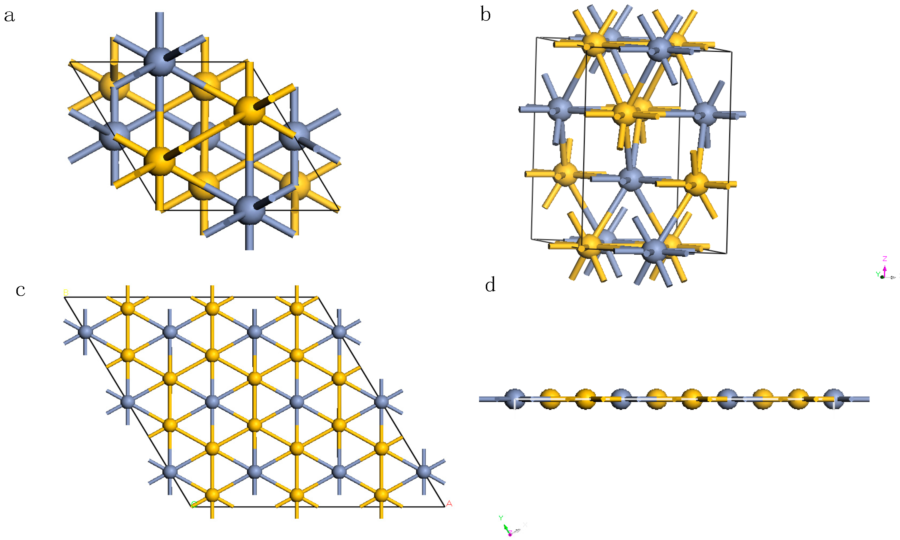
2. Material and Methods

Our calculations were performed using spin-polarized density functional theory (DFT) in the generalized gradient approximation (GGA) [35,36], with the Pedew-Burke-Ernzerhof (PBE) function for exchange-correlation potential, which were implemented in the Cambridge Sequential Total Energy Package (CASTEP) [37]. Projector augmented-wave (PAW) potentials [38] were employed to illustrate electron–ion interactions. The convergence criterion of total energy was set to be 10−6 eV, and energy cutoff of 310 eV was adopted for the expansion of plane waves after our test. The Monkhorst-Pack [39] k-point grids of 6 × 6 × 6, 6 × 6 × 1 were applied for the Brillouin-zone (BZ) integration in bulk, and monolayer CrSi2 computation, respectively. For monolayer CrSi2, vacuum-slabs of 15Å were used to avoid interactions between adjacent atom layers. CrSi2 has a hexagonal structure (C40) with nonsymmorphic space group D 6 4 -P6222 [24,25], containing no primitive translations which interchange individual CrSi2 layers. The lattice constants were a = 4.431 and c = 6.364 Å [24,25]. The lattice constants and atomic positions were fully relaxed until the force on each atom was less than 0.03 eV/Å. Monolayer CrSi2 has a graphene-like honeycomb structure, which can be formed by a micromechanical cleavage technique due to weak van der Waals (vdW) forces between those layers and strong covalent bonding intralayer [40]. Top and side views of monolayer CrSi2 after geometry optimization are depicted in Figure 1. According to chemical formula, per unit cell is constructed by one Cr atom and two Si atoms because in every intralayer, one Cr atom is in the center of each hexagonal hole of silicene lattice, leading to a 1:2 ratio between Cr and Si.

3. Results and Discussion

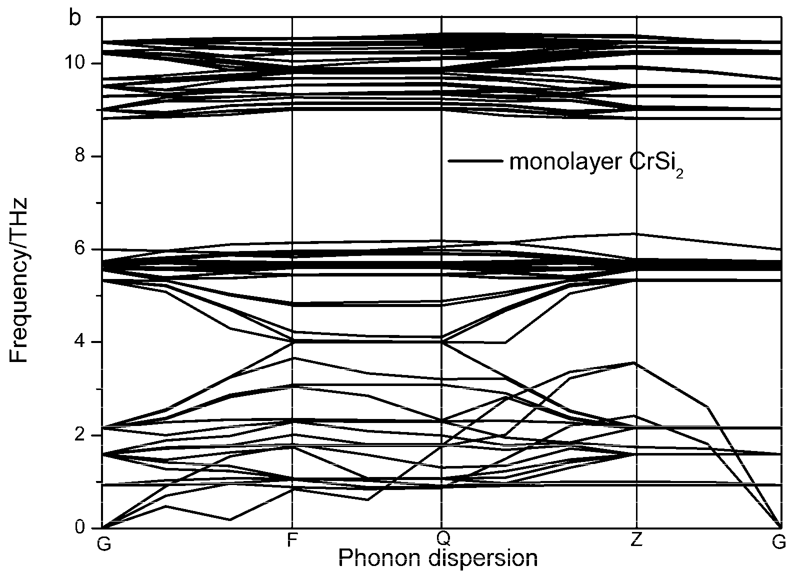
3.1. Phonon Dispersion Curve

It is necessary to check the structural stability of materials before calculation. Although the structures of bulk and monolayer CrSi2 have been optimized, the phase stability of these structures remains uncertain. Phonon dispersion spectrum analysis is a valid tool to confirm the structural stability. If all the phonon frequencies on the k-points in the Brillouin zone are positive, the structure is stable at absolute zero of temperature. Otherwise, the structure is unstable at absolute zero of temperature [41]. To check the structural stability of bulk and monolayer CrSi2, we accurately calculated phonon dispersion curves along the high symmetry directions in the Brillouin zone. As shown in Figure 2a for bulk CrSi2, and b for monolayer CrSi2, no imaginary vibration frequency appears for bulk and monolayer CrSi2, indicating that both structures of bulk and monolayer CrSi2 are stable at ground state in accordance with-Ref. [41].

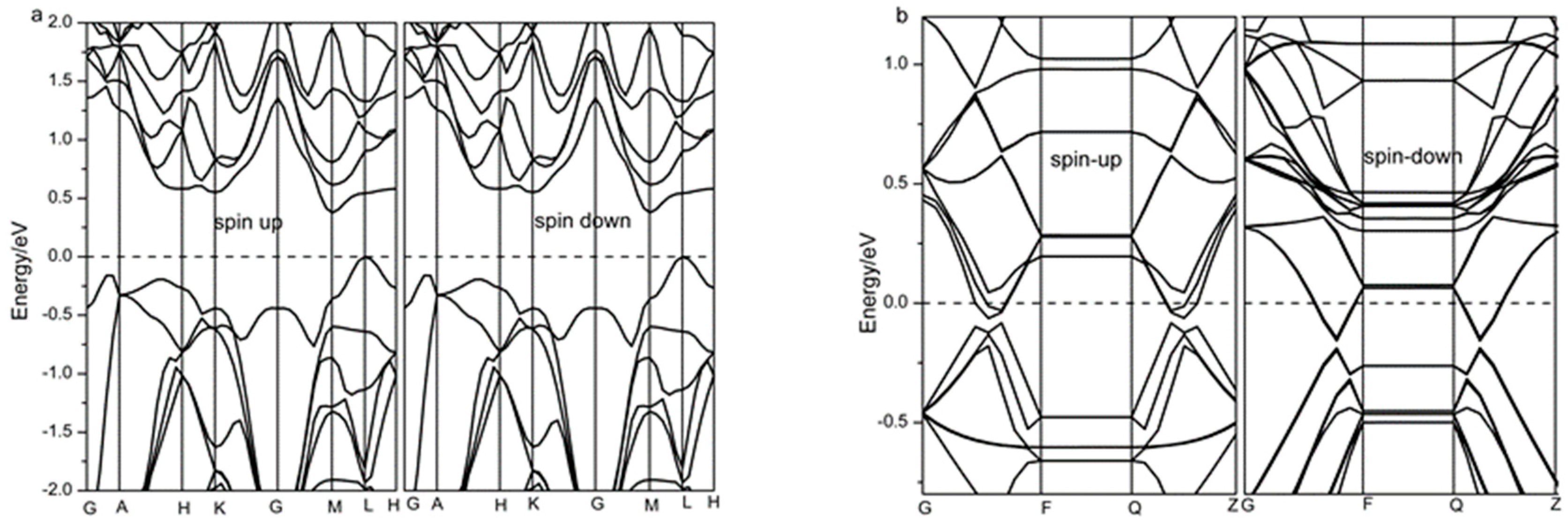
3.2. Electronic Structure

We calculated the magnetic moment of unit cell, local magnetic moment of Cr and Si atom, total energy, band length between Cr and Si atoms, band gap and lattice parameters, listed in Table 1. The results were satisfying, compared with those values calculated in References [9,24,25,29,30]. One can see that bulk CrSi2 is an indirect gap semiconductor, whereas, monolayer CrSi2 has metallic character. It can also be seen that there is a big difference between bulk and monolayer compounds in the magnetic moment, i.e., monolayer CrSi2 unit cell has an obvious magnetic moment~3.68 μ B , and the local magnetic moment of every Cr and Si atom were 4.11 and −0.21 μ B , respectively. In contrast, for the bulk CrSi2 system, every Cr and Si atom hardly had any magnetic moment. These results indicated that whilst bulk CrSi2 was diamagnetic, monolayer CrSi2 system was ferromagnetic (FM), consistent with the conclusions of References [9,10,11,29]. However, it conflicts with the results of Reference [30]. Unfortunately, until now, there is no available experimental evidence to validate the contradicting theoretical results. Potentially, this research may inspire more experimenters to study these two-dimensional systems.
To reveal the origin of metallicity and magnetism, band structure and total and partial density of states (DOS) were systematically studied. As shown in Figure 3, the band structures with up and down spin of bulk and monolayer CrSi2 are calculated. The results show that bulk CrSi2 is an indirect gap semiconductor with a band gap of 0.376 eV, which is in good accordance with Ref. [24,25], and monolayer CrSi2 is metallic being in good agreement with our previous results [10,11]. In the bulk CrSi2 system, the spin-up and spin-down states were completely symmetric, which indicated that bulk CrSi2 was a nonmagnetic semiconductor. However, for the monolayer CrSi2 system, the spin-up and spin-down states were in complete asymmetry and both spin-up and spin-down states go across the Fermi level, which manifested that monolayer CrSi2 was both magnetic and metallic. All these results were in good agreement with the analysis of Table 1. It has been confirmed that the energy band structure of TMDs are greatly affected by the crystal structure [20]. Huang et al. [42] have explored the origin of the high metallicity on MoSi2 nanofilms in detail. We can elucidate the physics mechanism of why bulk CrSi2 is a semiconductor, whilst monolayer CrSi2 is metallic using Huang’s theory. Both surface and confinement effects contribute to the high sensitivity of the metallicity on nanofilms type, explaining the reason why monolayer has a metallic character.
To further investigate the physical mechanism of magnetism, which may be dependent on the dimension of materials, we calculated the total density of states (DOS) and partial density of states (PDOS) of bulk and monolayer CrSi2 systems, as depicted in Figure 4. Total DOS and PDOS of the bulk CrSi2 system were fully symmetric, indicating that bulk CrSi2 system cannot have a magnetic characteristic, in accordance with Figure 3a. In contrast, for the monolayer CrSi2 system, both total DOS and PDOS of monolayer CrSi2 system were asymmetric, manifesting that monolayer CrSi2 system possesses a magnetic characteristic, in good agreement with Figure 3b. The degree of dissymmetry in PDOS of the Cr atom in monolayer CrSi2 system was greater than the Si atom’s, which is the reason why the Cr atom has a larger local magnetic moment as depicted in Table 1. In addition, the total density of state near Fermi level of the bulk CrSi2 system mainly consists of Cr-3d orbital electron. The total density of state near Fermi level of the monolayer CrSi2 system is mainly made up of Cr-3d orbital electron, with Cr-3p and Si-3p orbital electrons making limited contribution to the total density of state of the system. Moreover, the results also indicated that total magnetic moment (3.68 μB) arose mainly from the spin-up Cr-3d states. Han [9] has investigated the origin of magnetic behavior in monolayer FeSi2 and CoSi2 by orbital coupling of atoms. The stronger orbital coupling between atoms may account for the quench of magnetism of the atom. It can be seen from Figure 4b that no noticeable coupling between p orbital of Si atom and d orbital of Cr atom is found around the Fermi level, which indicates that monolayer CrSi2 has magnetic behavior.

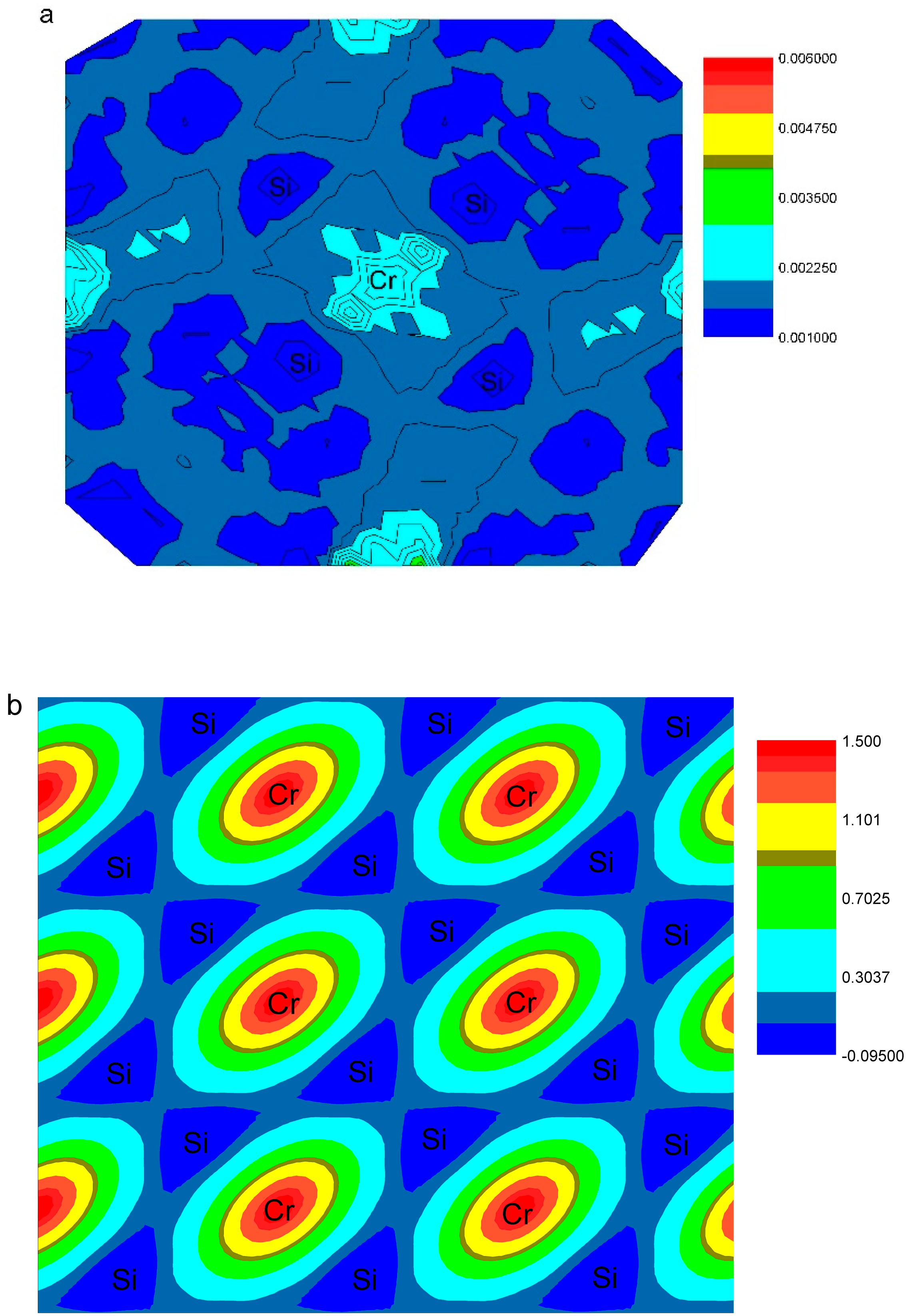
3.3. Magnetic Properties

To understand the origin of magnetism, which may be dependent on the dimension of the material, we further investigated the spin density of bulk and monolayer CrSi2 systems. As shown in Figure 5, the spin density isosurface plots of bulk and monolayer CrSi2 on top view (001) are particularly calculated. For the bulk CrSi2 system, spin density near Cr and Si atoms was close to zero, which agreed with the calculations of local magnetism moment of Cr and Si atoms (0 μ B ) in Table 1. Nevertheless, for the monolayer CrSi2 system, the numerical values of spin density near Cr atoms were very noticeable, which was much larger than those of spin density near Si atoms. It indicated that the behavior of magnetism in the monolayer was mainly contributed by the magnetic property of Cr atoms. Through careful analysis, we found that electron transfer from one Cr atom to one Si was equal in both the bulk and monolayer CrSi2 systems. The magnetic behavior has discrepancy in different dimension structures, which can be interpreted considering the charge transfer model [43] and Hund’s rules. The valence electron configurations of Cr and Si atoms are 3d54s1 and 3s23p2, respectively. In the bulk structure, every Cr (3d54s1) atom transfers one 4s electron and one 3d electron to adjacent two Si (3s23p2) atoms. Then, the Si atom whose electron configuration is 3s23p3 captures one electron to form a stable close-shell electronic structure, and thus has zero spin. The electron configuration of Cr atom is 3d4, which is an unstable electronic structure according to the octet rule. Owing to the van der Waals (vdW) force and chemical bonds energy between layers, valence electrons of Cr atom are antiparallel, as depicted in Figure 6a, leaving neither unpaired electrons nor net spin, which demonstrates that the Cr atom has no magnetic moment in the bulk CrSi2 system. This is slightly different from spin density, as depicted in Figure 5a, because it does not consider crystal field splitting. In the monolayer structure, valence electrons of Cr atom are parallel, as depicted in Figure 6b, which has the lowest energy due to the absence of the van der Waals (vdW) force and chemical bonds between layers, as well as the decline of chemical bonds energy in intralayer (i.e., the bond lengths increase, see Table 1), leaving unpaired electrons and net spin. This demonstrates that the Cr atom has magnetic moment in the monolayer CrSi2 system. Compared with the bulk material, electrons in the monolayer case favored occupying different orbits and having parallel spins, resulting in the monolayer case having less unfavorable Coulomb repulsion and lower energy. It was consistent with the Hund’s rules, that electrons always take precedence of different orbits and have the same spin direction occupying the equivalent orbital.
Owing to quantum size and surface effects, two-dimensional (2D) materials may present extensive novel physical and chemical properties, when downsizing from three dimensions to two dimensions or one dimension [20,21,22,23,44,45,46,47]. To further investigate the interrelationship between thickness and magnetism in CrSi2, we also calculated magnetic moment of unit cell of 2D multilayer nanosheets with different layers. The results depicted in Figure 7 show that the magnetic moment sharply decreases with the increase in the numbers of layers (especially, the magnetic moment decreases greatest when the number of layers increases from one layer to two layers). As the layers increase, the decrease of magnetic moments occurs in CrSi2 nanosheets. Considering weak van der Waals force and strong chemical bonds between layers, quantum size [20,21,22,23,46] and surface effects [44] occur when downsizing from bilayers to monolayer in CrSi2 nanosheets. We deduced that the band energy between layers, as well as quantum size and surface effects play an important role in magnetism of materials. Magnetic response of 2D materials can be tuned by controlling the thinness of thin films, which is an advantageous application in magnetic materials.

4. Conclusions

Electronic and magnetic properties of CrSi2 were calculated using the first-principle methods based on density functional theory. The phonon dispersion curve, band structures with spin state, total and partial density of states (DOS), and spin density of bulk and monolayer CrSi2 systems were systematically investigated. Both bulk and monolayer CrSi2 were structurally stable at ground state. The results showed that the bulk CrSi2 system is an indirect gap non-magnetic semiconductor with a band gap of 0.376 eV, whilst the monolayer CrSi2 sheets were metallic and ferromagnetic (FM). Compared with previous literature, our results were consistent with Dzade’s results (ferromagnetism) and inconsistent with Bui’s results (anti-ferromagnetism). We explain the reason why monolayer CrSi2 had metallic behavior using Huang’s theory, where surface and confinement effects play an important role in the metallic behavior of monolayer CrSi2. Further analysis showed that total DOS and PDOS of the bulk CrSi2 system were fully symmetric, and those of the monolayer CrSi2 system were asymmetric, which may reveal the physical mechanism of magnetism for bulk and CrSi2 nanosheets. In addition, we also elucidated the origin of magnetism considering the charge transfer model and Hund’s rules, where magnetic moment of unit cell of 2D multilayer nanosheets with different layers was calculated. The results showed that the magnetism of materials is attributed to band energy between layers, as well as quantum size and surface effects. We also expect that our calculations may provide some helpful insight into further experimental investigations, and they show promise in device applications based on 2D CrSi2 nanosheets.

Author Contributions

Conceptualization, S.C.; Methodology, Y.C. and X.Q.; Software, S.C. and Y.C.; Formal Analysis, W.Y., S.Z., and W.X.; Data Curation, S.C.; Writing-Original Draft Preparation, S.C.; Writing-Review & Editing, S.C., L.L., and W.X.; Supervision, Y.C.

Funding

This research was funded by [Key Projects of the Tripartite Foundation of Guizhou Science and Technology Department] grant number [[2015]7696], and by [Guizhou College Student Innovation Entrepreneurship Training Program] grant number [201710667017], and by [Major Projects for Creative Research Groups of Guizhou Province of China] grant number [[2016]048], and by [Innovation Team of Anshun University] grant number [2015PT02], and by [Natural Science Foundation of Science and Technology Department of Guizhou Province of China] grant number [[2010]2001].

Acknowledgments

We are really grateful to the cloud computing platform at Guizhou University and the CNROCK HOLE BLACKHOLE high density computing platform for computing support.

Conflicts of Interest

The authors declare no conflict of interest.

References

  1. Novoselov, K.S.; Geim, A.K.; Morozov, S.V.; Jiang, D.; Zhang, Y.; Dubonos, S.V.; Grigorieva, I.V.; Firsov, A.A. Electric field effect in atomically thin carbon films. Science 2004, 306, 666–669. [Google Scholar] [CrossRef] [PubMed]
  2. Xu, M.S.; Liang, T.; Shi, M.M.; Chen, H.Z. Graphene-like two-dimensional materials. Chem. Rev. 2013, 113, 3766–3798. [Google Scholar] [CrossRef] [PubMed]
  3. Lew Yan Voon, L.C.; Guzmán-Verri, G.G. Is silicone the next graphence. MRS Bull. 2014, 39, 366–373. [Google Scholar] [CrossRef]
  4. Kara, A.; Enriquez, H.; Seitsonen, A.P.; Lew Yan Voon, L.C.; Vizzini, S.; Aufray, B.; Oughaddou, H. A review on silicone-new candidate for electronics. Sur. Sci. Rep. 2012, 67, 1–18. [Google Scholar] [CrossRef]
  5. Golberg, D.; Bando, Y.; Huang, Y.; Terao, T.; Mitome, M.; Tang, C.; Zhi, C. Boron nitride nanotubes and nanosheets. ACS Nano 2010, 4, 2979–2993. [Google Scholar] [CrossRef] [PubMed]
  6. Pakdel, A.; Zhi, C.; Bando, Y.; Golberg, D. Low-dimensional boron nitride nanomaterials. Mat. Today 2012, 15, 256–265. [Google Scholar] [CrossRef]
  7. Chhowalla, M.; Shin, H.S.; Eda, G.; Li, L.J.; Loh, K.P.; Zhang, H. The chemistry of two-dimensional layered transition metal dichalcogenidenanosheets. Nat. Chem. 2013, 5, 263–275. [Google Scholar] [CrossRef] [PubMed]
  8. Butler, S.Z.; Hollen, S.M.; Cao, L.; Cui, Y.; Gupta, J.A. Progress, challenges, and opportunities in two-dimensional materials beyond grapheme. ACS Nano 2013, 7, 2898–2926. [Google Scholar] [CrossRef] [PubMed]
  9. Han, N.N.; Liu, H.S.; Zhao, J.J. Novel magnetic monolayers of transition metal silicide. J. Superconduct. Nov. Magn. 2015, 28, 1755–1758. [Google Scholar] [CrossRef]
  10. Chen, S.B.; Chen, Y.; Yan, W.J.; Zhou, S.Y.; Xiong, W.; Yao, X.X.; Qin, X.M. Magnetism and optical property of Mn-doped monolayer CrSi2 by first-principle study. J. Superconduct. Nov. Magn. 2017. [Google Scholar] [CrossRef]
  11. Chen, S.B.; Zhou, S.Y.; Yan, W.J.; Chen, Y.; Qin, X.M.; Xiong, W. Effect of Fe and Ti Substitution Doping on Magnetic Property of Monolayer CrSi2: A first-principle investigation. J. Superconduct. Nov. Magn. 2018. [Google Scholar] [CrossRef]
  12. Han, W.; Kawakami, R.K.; Gmitra, M.; Fabian, J. Graphene spintronics. Nat. Nanotechnol. 2014, 59, 794–807. [Google Scholar] [CrossRef] [PubMed]
  13. Maassen, J.; Ji, W.; Guo, H. Graphene spintronics: The role of ferromagnetic electrodes. Nano Lett. 2011, 11, 151–155. [Google Scholar] [CrossRef] [PubMed]
  14. Fuh, H.R.; Chang, K.W.; Hung, S.H.; Jeng, H.T. Two-dimensional magnetic semiconductors based on transition-metal dichalcogenides VX2 (X=S, Se, Te) and similar layered compounds VI2 and Co(OH)2. IEEE Magn. Lett. 2017, 8, 3101405. [Google Scholar] [CrossRef]
  15. Das Sarma, S.; Adam, S.; Hwang, E.H.; Rossi, E. Electronic transport in two dimensional graphene. Rev. Mod. Phys. 2011, 83, 407–470. [Google Scholar] [CrossRef]
  16. Parkin, S.; Yang, S.H. Memory on the racetrack. Nat. Nanotechnol. 2015, 10, 195–198. [Google Scholar] [CrossRef] [PubMed]
  17. Parkin, S.S.P.; Hayashi, M.; Thomas, L. Magnetic domain-wall racetrack memory. Science 2008, 320, 190–194. [Google Scholar] [CrossRef] [PubMed]
  18. Eda, G.; Fujita, T.; Yamaguchi, H.; Voiry, D.; Chen M Chhowalla, M. Coherent atomic and electronic heterostructures of single-layer MoS2. ACS Nano 2012, 6, 7311–7317. [Google Scholar] [CrossRef] [PubMed]
  19. Ci, L.; Song, L.; Jin, C.; Jariwala, D.; Wu, D.; Li, Y. Atomic layers of hybridized boron nitride and graphene domains. Nat. Mater. 2010, 9, 430–435. [Google Scholar] [CrossRef] [PubMed]
  20. Zhang, H.; Liu, L.M.; Lau, W.M. Dimension-dependent phase transition and magnetic properties of VS2. J. Mater. Chem. A 2013, 1, 10821–10828. [Google Scholar] [CrossRef]
  21. Abdul Wasey, A.H.M.; Soubhik, C.; Das, G.P. Quantum size effects in layered VX2 (X=S, Se) materials: Manifestation of metal to semimetal or semiconductor transition. J. Appl. Phys. 2015, 117, 064313. [Google Scholar] [CrossRef]
  22. Tan, C.L.; Sun, D.; Tian, X.H.; Huang, Y.W. First-principles investigation of phase stability, electronic structure and optical properties of MgZnO monolayer. Materials 2016, 9, 877. [Google Scholar] [CrossRef] [PubMed]
  23. Wang, W.D.; Bai, L.W.; Yang, C.G.; Fan, K.Q.; Xie, Y.; Lin, M.L. The electronic properties of O-doped pure and sulfur vacancy-defect monolayer WS2: A first-principles study. Materials 2018, 11, 218. [Google Scholar] [CrossRef] [PubMed]
  24. Krijn, M.P.C.M.; Eppenga, R. First-principles electronic structure and optical properties of CrSi2. Phys. Rev. B 1991, 44, 9042–9044. [Google Scholar] [CrossRef]
  25. Mattheiss, L.F. Electronic structure of CrSi2 and related refractory disilicides. Phys. Rev. B 1991, 43, 12549–12555. [Google Scholar] [CrossRef]
  26. Dasgupta, T.; Etourneau, J.; Chevalier, B.; Matar, S.F.; Umarji, A.M. Structural, thermal, and electrical properties of CrSi2. J. Appl. Phys. 2008, 103, 113516. [Google Scholar] [CrossRef]
  27. Singh, D.J.; Parker, D. Itinerant magnetism in doped semiconducting β-FeSi2 and CrSi2. Sci. Rep. 2013, 3, 3517. [Google Scholar] [CrossRef] [PubMed]
  28. Parker, D.; Singh, D.J. Very heavily electron-doped CrSi2 as a high performance high-temperature thermoelectric material. New J. Phys. 2012, 14, 033045. [Google Scholar] [CrossRef]
  29. Dzade N, Y.; Obodo, K.O.; Adjokatse, S.K. Silicene and transition metal based materials: Prediction of a two dimensional piezomagnet. J. Phys. Condens. Matter. 2010, 22, 375502–375509. [Google Scholar] [CrossRef] [PubMed]
  30. Viet Q, B.; Pham, T.T.; Nguyen, H.V.S.; Le, H.M. Transition metal (Fe and Cr) adsorptions on buckled and planar silicene monolayers: A density functional theory investigation. J. Phys. Chem. C 2013, 117, 23364–23371. [Google Scholar]
  31. Wang, X.Q.; Li, H.D.; Wang, J.T. Induced ferromagnetism in one-side semihydrogenated silicene and germanene. Phys. Chem. Chem. Phys. 2012, 14, 3031–3036. [Google Scholar] [CrossRef] [PubMed]
  32. Zhang, C.W.; Yan, S.S. First-principles study of ferromagnetism in two-dimensional silicene with Hydrogenation. J. Phys. Chem. C 2012, 116, 4163–4166. [Google Scholar] [CrossRef]
  33. Kaloni, T.P.; Gangopadhyay, S.; Singh, N.; Jones, B. Electronic properties of Mn-decorated silicene on hexagonal boron nitride. Phys. Rev. B 2013, 88, 235418. [Google Scholar] [CrossRef] [Green Version]
  34. Zhu, H.N.; Gao, K.Y.; Liu, B.X. Formation of n-type CrSi2 semiconductor layers on Si by high-current Cr ion implantation. J. Phys. D Appl. Phys. 2000, 33, L49–L52. [Google Scholar] [CrossRef]
  35. Perdew, J.P.; Burke, K.; Ernzerhof, M. Generalized gradient approximation made simple. Phys. Rev. Lett. 1996, 77, 3865–3868. [Google Scholar] [CrossRef] [PubMed]
  36. Payne, M.C.; Teter, M.P.; Allan, D.C.; Arias TA Joannopoulos, J.D. Iterative minimization techniques for ab initio total-energy calculations: Molecular dynamics and conjugate gradients. Rev. Mod. Phys. 1992, 64, 1064–1096. [Google Scholar] [CrossRef]
  37. Clark, S.J. First principles methods using CASTEP. Z. Kristall. 2005, 220, 567–570. [Google Scholar] [CrossRef] [Green Version]
  38. Kresse, G.; Joubert, D. Self-interaction correction to density-functional approximations for many-electron systems. Phys. Rev. B Condens. Matter Mater. Phys. 1999, 59, 1758–1775. [Google Scholar] [CrossRef]
  39. Monkhorst, H.J.; Pack, J.D. Special points for Brillouin-zone integrations. Phys. Rev. B 1976, 13, 5188–5192. [Google Scholar] [CrossRef]
  40. Zeng, Z.Y.; Yin, Z.Y.; Huang, X.; Li, H.; He, Q.Y.; Lu, G.; Boey, F.; Zhang, H. Single-layer semiconducting nanosheets: High-yield preparation and device fabrication. Angew. Chem. Int. Ed. 2011, 50, 11093–11097. [Google Scholar] [CrossRef] [PubMed]
  41. Hermet, P.; Khalil, M.; Viennois, R.; Beaudhuin, M.; Bourgogne, D.; Ravot, D. Revisited phonon assignment and electromechanical properties of chromium disilicide. RSC Adv. 2015, 5, 19106–19116. [Google Scholar] [CrossRef]
  42. Huang L, F.; Rondinelli, J.M. Stable MoSi2 nanofilms with controllable and high metallicity. Phys. Rev. Mater. 2017, 1, 063001-1–063001-6. [Google Scholar] [CrossRef]
  43. Chen, Q.; Wang, J.L. Structural, electronic, and magnetic properties of TMZn11O12 and TM2Zn10O12 clusters (TM = Sc, Ti, V, Cr, Mn, Fe, Co, Ni, and Cu). Chem. Phys. Lett. 2009, 474, 336–341. [Google Scholar] [CrossRef]
  44. Li, H.; Qi, X.; Wu, J.; Zeng, Z.; Wei, J.; Zhang, H. Investigation of MoS2 and graphene nanosheets by magnetic force microscopy. ACS Nano 2013, 7, 2842–2849. [Google Scholar] [CrossRef] [PubMed]
  45. Tongay, S.; Varnoosfaderani, S.S.; Appleton, B.R.; Wu, J.Q.; Hebard, A.F. Magnetic properties of MoS2: Existence of ferromagnetism. Appl. Phys. Lett. 2012, 101, 123105. [Google Scholar] [CrossRef]
  46. Li, X.M.; Tao, L.; Chen, Z.F.; Fang, H.; Li, X.S.; Wang, X.R.; Xu, J.B.; Zhu, H.W. Graphene and related two-dimensional materials: Structure-property relationships for electronics and optoelectronics. Appl. Phys. Rev. 2017, 4, 021306. [Google Scholar] [CrossRef] [Green Version]
  47. Li, Z.Q.; Chen, F. Ion beam modification of two-dimensional materials: Characterization, properties, and applications. Appl. Phys. Rev. 2017, 4, 011103. [Google Scholar] [CrossRef]
Figure 1. Top and side views of bulk and monolayer CrSi2 after geometry optimization. Figure 1a,b describe top view and side view of the bulk CrSi2 crystalline structure, Figure 1c,d depict top view and side view of the monolayer CrSi2 crystalline structure, respectively. Yellow balls and blue balls represent Si and Cr atoms.
Applsci 08 01885 g001
Figure 2. Phonon dispersion curves along the high-symmetry directions in the Brillouin zone of (a) bulk CrSi2, (b) monolayer CrSi2.
Applsci 08 01885 g002aApplsci 08 01885 g002b
Figure 3. Band structure with spin-up and spin-down of (a) bulk and (b) monolayer CrSi2.
Applsci 08 01885 g003
Figure 4. Total and partial density of states (DOS) varies from the energy for (a) bulk and (b) monolayer CrSi2.
Applsci 08 01885 g004
Figure 5. Spin density iso-surface plots of (a) bulk and (b) monolayer CrSi2 on top view (001). The iso-surface level is set as 0.003e/Å3.
Applsci 08 01885 g005
Figure 6. Valence electron diagrams of Cr atom in (a) bulk and (b) monolayer CrSi2 systems.
Applsci 08 01885 g006
Figure 7. The magnetic moment of unit cell of multilayer CrSi2 nanosheets varies with different layers.
Applsci 08 01885 g007
Table 1. Magnetic moment and structure of bulk and monolayer CrSi2.
Magnetic   Moment   of   Unit   Cell   ( μ B ) Local   Magnetic   Moment   of   Cr   Atom   ( μ B ) Local   Magnetic   Moment   of   Si   Atom   ( μ B ) Total Energy of System (ev)Band Length of cr-si of Intralayer (å)Band Gap (eV)Lattice Parameter (Å)
bulk CrSi24 × 10−400−8050.322.47, 2.52,2.550.376a = 4.4276
c = 6.3681
0 c0 c0 c--2.47 a, 2.55 a, 3.06 a0.35 a, 0.21 da = 4.42 a, 4.43 d
c = 6.349 a, 6.36 d
monolayer CrSi23.684.11−0.21−24118.242.550a = 4.4276
c = 15
3.6 b4.15 c----2.56 b0 ca = 3.93968 e
c = 16.49899 e
a Reference [25]. b Reference [29]. c Reference [30]. d Reference [24]. e Reference [9].

