Article

Performance of Nanostructures within InGaN-Based Multiquantum-Well Light-Emitting Devices

1
Department of Electronic Engineering, Ming Chi University of Technology, New Taipei City 243, Taiwan
2
College of Engineering, Chang Gung University, Taoyuan 333, Taiwan
3
Department of Electrical Engineering, Taipei City University of Science and Technology, Taipei 112, Taiwan
*
Author to whom correspondence should be addressed.
Appl. Sci. 2017, 7(4), 380; https://doi.org/10.3390/app7040380
Submission received: 26 January 2017 / Revised: 6 April 2017 / Accepted: 10 April 2017 / Published: 11 April 2017

Abstract

:
We introduced multiquantum-barrier (MQB) nanostructures into the barrier layers of InGaN/GaN multiquantum-well (MQW) heterostructures to improve the operation characteristics of the light-emitting devices. The electroluminescence (EL) spectra were examined over a broad range of temperatures for the samples. We observed inhibited carrier leakage for the sample with the MQB nanostructures. Greater inhomogeneity of nanocrystallite size and a stronger localization effect were also observed for the sample. To interpret this phenomenon, high-resolution X-ray diffraction curves were measured and analyzed using the Warren–Averbach model. External quantum efficiency as a function of temperature was also evaluated. The calculation results correspond with the inference the EL measurements provided. We determined that the performance of the light-emitting devices is enhanced by the MQB nanostructures within InGaN/GaN MQWs.

1. Introduction

III–N compound semiconductors have been used in a wide range of applications because of their broad applications in the fabrication of light-emitting diodes (LEDs), laser diodes (LDs), solar cells, and photodetectors, which emit over a broad spectral range from infrared to ultraviolet [1,2,3]. Much interest has been focused on InGaN/GaN multiquantum wells (MQWs) because they can act as the active layer in high-brightness III-N LEDs and blue and green LDs [3,4]. For conventional LEDs, the quantum-confined Stark effect (QCSE) due to the large strain-induced polarization field reduces the overlap integral between the electron and hole wave functions, thereby reducing radiative recombination rates and related radiative efficiency. Some methods have been suggested to address the reduced overlap integral between the electron and hole wave functions, including polarization band engineering [5], developing InGaN LEDs on GaN templates with nonpolar or semipolar crystal orientations [6,7]; thus, the improvement of internal quantum efficiency can be achieved. A significant improvement of device efficiency has recently made rapid progress in LED development [8,9].
For lighting applications, InGaN/GaN MQW devices must deal with the requirements of high current injection. However, their performance decreases significantly as the operating current density increases. Several mechanisms have been suggested to explain the efficiency droop, including Auger recombination [10,11,12,13], carrier delocalization from In-rich low-defect-density regions at high carrier densities [14,15], and carrier leakage at high forward currents [16]. It was reported that Auger recombination plays an important role in the efficiency droop of MQW LEDs at high current density, a dilute-As GaNAs material with negligible interband Auger process was proposed recently as a possible material to solve the problem [10,11,12,13]. In addition, the performance of such devices is also limited by the loss of electrons overflowing from the active layer to the nonradiative recombination centers under high current density [17]. In this study, we introduced a multiquantum-barrier (MQB) nanostructure instead of a conventional GaN barrier into the InGaN-based MQWs to improve the performance of the devices. Temperature-dependent electroluminescence (EL) measurements were conducted over a temperature range from 20 to 380 K and an injection current level from 10 to 100 mA. A higher EL spectra intensity and an extended energy scale of potential fluctuations were obtained for the sample with MQB nanostructures. High-resolution X-ray diffraction (HRXRD) spectra were measured and analyzed using a theoretical model to further characterize the nanocrystallites in the samples. Moreover, the external quantum efficiency of the samples was compared. The results indicate that the operation of InGaN/GaN MQW light-emitting devices is improved because of the nanostructures within InGaN/GaN MQW barrier layers.

2. Experiments

The samples studied in this work were grown using metalorganic vapor phase epitaxy (MOVPE) on c-plane sapphire substrates. The layer structure of the sample with conventional barrier layers in MQWs consisted of a 20-nm-thick GaN buffer layer, a 3-μm-thick n-type GaN layer, an undoped GaN layer possessing five periods of In0.18Ga0.82N/GaN MQWs, and a 100-nm-thick p-type GaN layer. The thicknesses of the InGaN wells and the GaN barriers in the MQW structures were 2 nm and 11 nm, respectively. For the sample with MQB nanostructures, the layer structure was similar, but only with five periods of In0.15Ga0.85N/GaN MQWs, and the barrier layer of MQW was replaced with a five-period In0.02Ga0.98N/GaN (1 nm/1 nm) heterostructure. After growth, the epilayers were characterized through HRXRD. Rocking curves appeared in the (002) reflection produced using the Bede D1 system. The temperature-dependent EL measurements were conducted after mounting the sample in a closed-cycle helium cryostat where the temperature (T) was varied from 20 to 380 K and using a current source operated from 10 to 100 mA. The luminescence signal was dispersed through a 0.5 m monochromator and detected by using a silicon photodiode by the standard lock-in amplification technique.

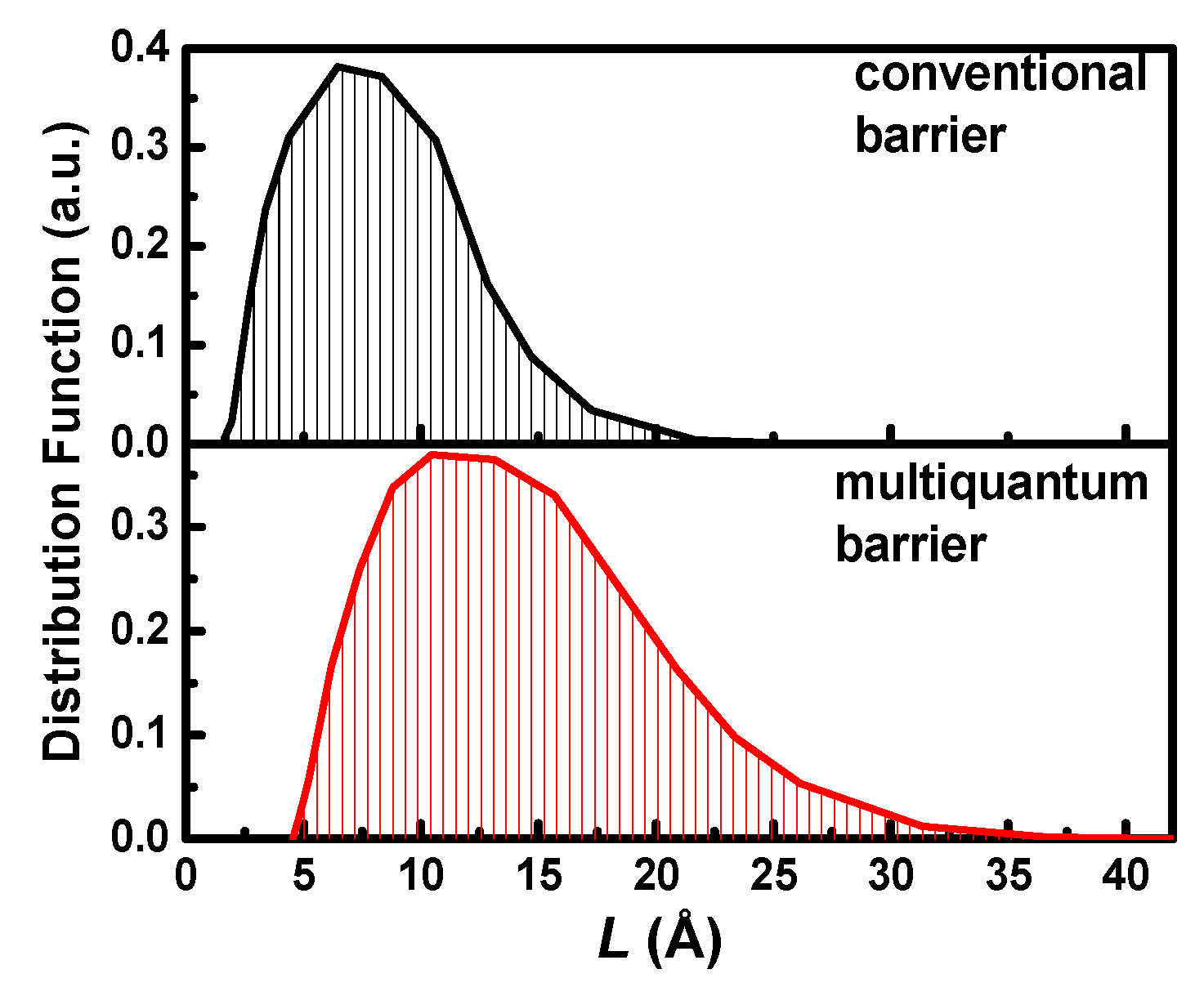
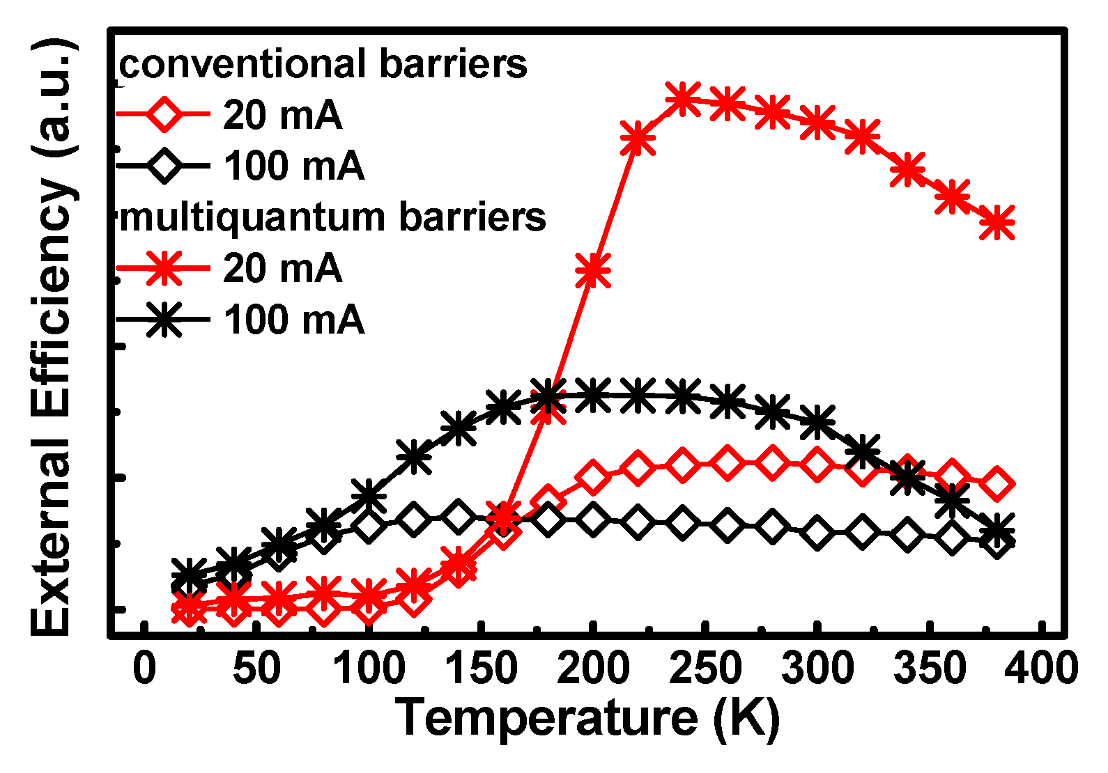
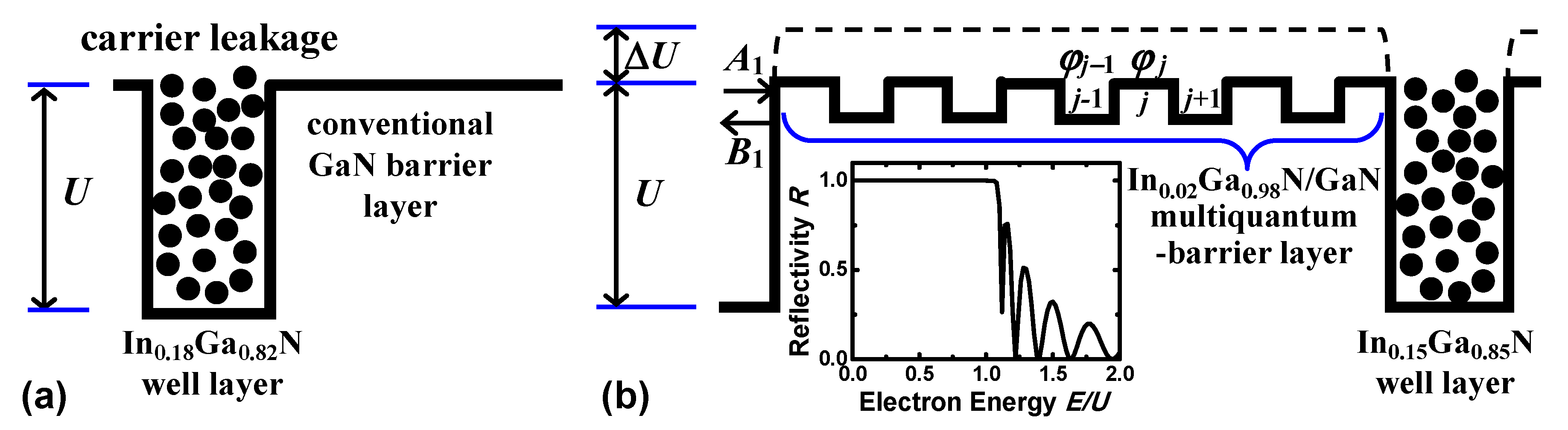
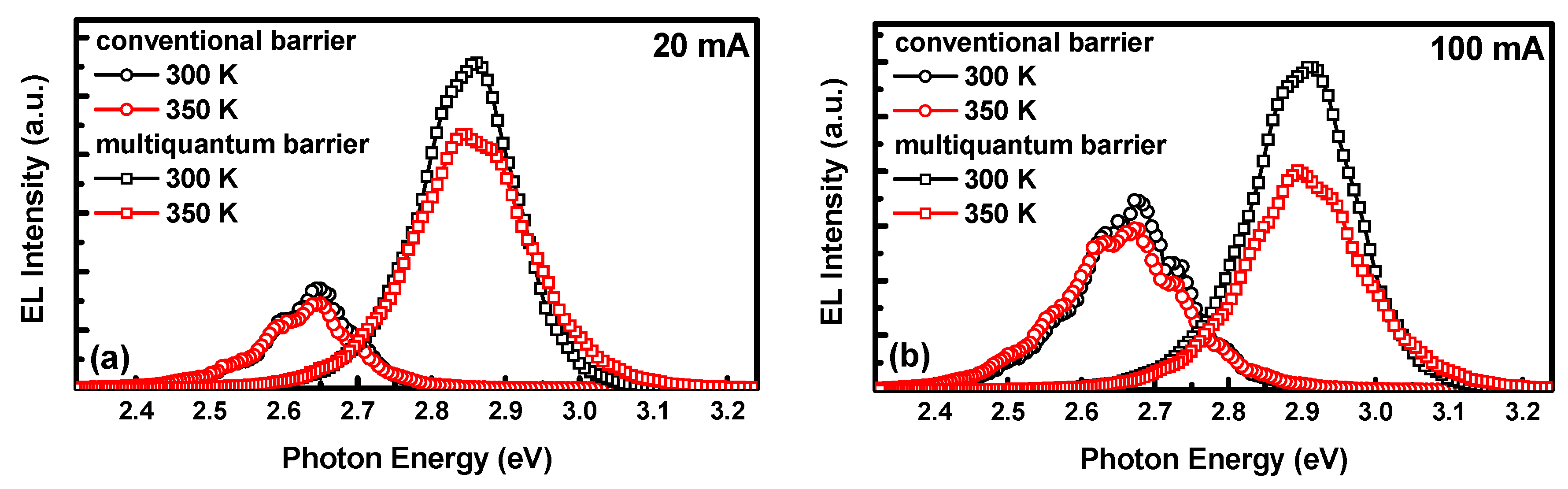
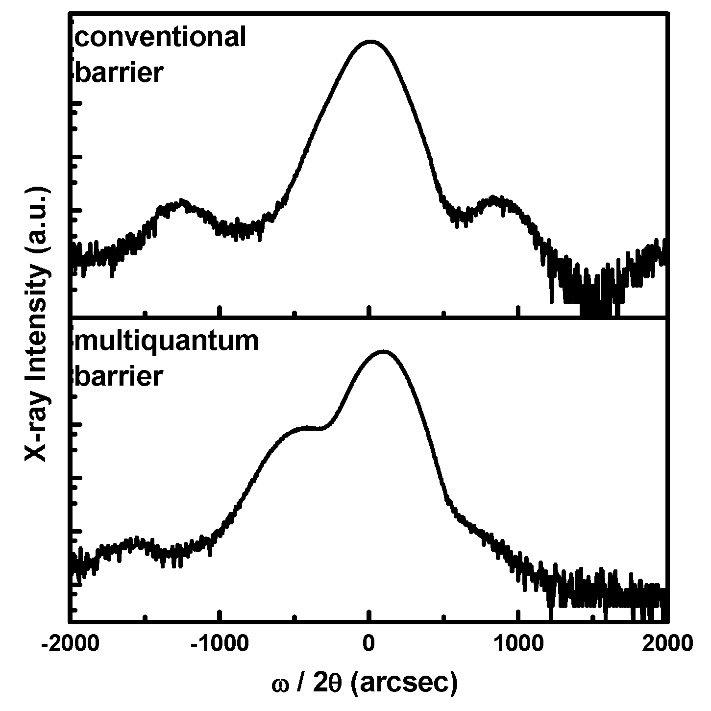
3. Results and Discussion

Figure 1 schematically represents the structures of the samples investigated in this study. The MQB structure shown in Figure 1b is engineered to align a forbidden energy miniband of the MQB superlattice with the conduction band minimum to enhance conduction band discontinuity [18,19,20]. For the MQB structure, the electron wave function of the jth layer can be calculated by solving a one-dimensional Schrödinger equation, and is expressed as
φ j ( x ) = A j e x p ( i k j x ) + B j e x p ( i k j x ) .
kj denotes the wave number in the jth layer and
k j = 2 m j ( E V j ) / ,
where m j is the electron effective mass in the jth layer, E is the energy of an electron, and Vj is the potential height of the jth layer. By matching the wave functions and their first derivatives divided by the effective mass at each interface, we obtain
φ j 1 ( x j 1 ) = φ j ( x j 1 ) ,
1 m j 1 d φ j 1 d x   = 1 m j d φ j d x  
Considering the coupling between the incident wave functions and the outgoing wave functions through the MQBs, the reflectivity probability R against incident electron energy is defined as
R = | B 1 / A 1 | 2 ,
which can be obtained by the transfer matrix method [21,22]. According to the method, the layer structure which includes an In0.15Ga0.85N well layer and a five-period In0.02Ga0.98N/GaN barrier layer is calculated. In the simulation, the conduction discontinuity for InGaN-GaN is assumed to be approximately 62% of the band gap difference ∆Eg. Following the linear Vegard’s law, the bandgap and the electron effective mass that we used in the simulation were 3.03 eV and 0.1865 m0, respectively, for In0.15Ga0.85N; 3.43 eV and 0.1982 m0 respectively, for In0.02Ga0.98N, where m0 is the free electron mass. Due to the interference effect, the MQB structures characteristically exhibit regions of high reflectivity for electrons with energy above the bulk potential barrier. The simulated result shown in Figure 1b illustrates that a band of nonallowed electron states is created above the classical barrier height by 1.08 times relative to the conventional GaN barrier. Because the MQB nanostructure increases the band discontinuity, it is expected to prevent the electrons from overflowing as operated at high temperatures and high driving currents. Observing the EL spectra of the samples measured at 300 K and 350 K and at injection current of 20 mA and 100 mA shown in Figure 2, the higher EL spectra intensity for the sample with MQBs provides evidence of the improvement of carrier confinement and inhibited carrier leakage in the active layer. Moreover, the emission peak energies for sample with MQBs are larger than those of sample with conventional GaN barriers. Considering the lesser indium composition in the well layer and the indium content in the barrier layer for the MQB sample, the smaller polarization charges and the reduced internal field in the well layer can be achieved [23]. The reduced polarization field leads to an increased electron–hole wave function overlap, which also enhances the EL peak intensity and results in larger EL peak energies for the MQB sample.
The evolution of EL spectra for the sample with conventional GaN barriers over a temperature range from 20 to 380 K is shown in Figure 3a. The temperature dependence of the peak energy does not follow Varshni’s law. The “S-shaped” temperature dependence of the EL peak energy is the fingerprint of the existence of localized band-tail states [24,25]. At low temperatures, carriers are randomly distributed among the potential minima caused by the inhomogeneous potential fluctuations. As the temperature slightly increases, the carriers gain sufficient thermal energy to overcome small potential barriers and relax into lower energy tail states where the radiative recombination finally takes place. In the mid-temperature range, the blueshift of the peak energy is a result of the thermal population of higher energy states of the density of states [26,27]. Here a transition from the localized states in the quantum well takes place. As the temperature is even higher, the blueshift behavior is smaller than the temperature-induced band-gap shrinkage, thus the peak position exhibits a redshift behavior. A similar thermal action is conducted for the sample with MQBs, as shown in Figure 3b. The amounts of blueshift of peak energy are 40.4 and 46.7 meV for the samples with the GaN barrier and with MQBs, respectively, implying a wider energy scale distribution of the band potential profile fluctuations and a stronger localization effect for the MQB sample.
In InGaN/GaN MQWs, the indium compositional inhomogeneity causes potential fluctuations, which has been proposed as the cause of the localization effect [28,29]. Analysis of the contribution of structure-related heteropotential fluctuations on the recombination mechanisms show that a compositionally inhomogeneous InGaN/GaN heterosystem can be regarded as a partially disordered structure. The nanostructures of InGaN/GaN MQWs can be viewed as disordered collections of InGaN nanocrystallites. To determine the size distribution of the nanocrystallites, we investigated the HRXRD line profile of the samples. Figure 4 shows the measured XRD patterns of the samples. The major peaks and the shoulders on the left correspond to the features of GaN and InGaN, respectively. Superlattice satellite peaks emerging from the InGaN thin layer are indicative of indium incorporation in the barriers. For the sample with multiquantum barriers, the XRD linewidths were observed to broaden, indicating crystalline randomization and interface roughness of the sample. To determine the size distribution of nanocrystallites in our samples, the XRD spectra were analyzed using the Warren–Averbach method in Fourier space [30,31], and the calculation results are shown in Figure 5. We can see that the sample with multiquantum barriers exhibits a wider breadth of nanocrystallite size distribution. The broader nanocrystallite size distribution implies that fluctuation in the overall composition is enhanced for the sample with MQBs, coinciding with the inferences derived from the EL measurements.
The effect of MQB nanostructures on the operation of the light-emitting devices is further investigated by discussing the EL efficiency of the samples. To show the variations in EL efficiency at increasing temperatures, the integrated EL intensity is divided by the injection current, which is proportional to the EL external quantum efficiency. The calculated result of the samples is shown in Figure 6. With the injection current of 20 mA, it is clearly seen that the EL efficiency of the sample with MQBs is significantly higher than that of the sample with GaN barriers. The improved performance of the light-emitting device can be attributed to the enhanced fluctuation in the overall indium composition of the sample with MQBs, which causes a stronger localization effect in the active layer and a better carrier spreading of the device [32]. Besides, with indium content in the barrier layer for the MQB sample, the polarization field in the well layer was reduced [23,33,34]. The reduced polarization field increases the electron–hole wave function overlap and results in a raised EL efficiency. Moreover, the increased conduction band discontinuity and the enhancement of carrier confinement may also give a contribution to the EL efficiency. As the injection current was increased to 100 mA, a higher EL efficiency for the sample with MQBs was also obtained; nevertheless, the efficiency degraded as the temperature increased above 320 K. Thanks to crystal quality decreases with the degree of the overall potential fluctuations in the InGaN composition, this sample exhibits more nonradiative recombination centers, which caused an intensity quenching at high temperature and high injection current level. Actually, even operated at high injection current, the EL external quantum efficiency of the MQB sample was obviously higher than that of the sample with GaN barriers at room temperature.

4. Conclusions

In this study, we investigated the performance of InGaN/GaN MQW light-emitting devices with conventional GaN barriers and with multiquantum barriers by measuring EL spectra over a broad range of temperatures and injection currents. We observed an enhancement of carrier confinement in the active layer and a broadened energy-scale distribution of potential fluctuations for the sample with MQBs. The measured HRXRD line profiles were analyzed using the Warren–Averbach model, and the inference confirms our results. From the evaluation of temperature-dependent external quantum efficiency under different injection currents, the efficiency of the sample with MQBs was found to be significantly higher than that of the sample with conventional GaN barriers. The MQB nanostructures profoundly improve the operation of light-emitting devices.

Author Contributions

Ya-Fen Wu conceived and designed the experiments, analyzed the data, and wrote the paper. Jiunn-Chyi Lee performed the experiments and analyzed the data.

Conflicts of Interest

The authors declare no conflict of interest.

References

  1. Nakamura, S.; Fasol, G. The Blue Laser Diode; Springer: Berlin, Germany, 1997. [Google Scholar]
  2. Nakamura, S.; Senoh, M.; Nagahama, S.I.; Iwasa, N.; Yamada, T.; Matsushita, T.; Kiyoku, H.; Sugimoto, Y. InGaN-Based Multi-Quantum-Well-Structure Laser Diodes. Jpn. J. Appl. Phys. 1996, 35, L74–L76. [Google Scholar] [CrossRef]
  3. Zhang, M.; Bhattacharya, P.; Guo, W. InGaN/GaN self-organized quantum dot green light emitting diodes with reduced efficiency droop. Appl. Phys. Lett. 2010, 97, 011103. [Google Scholar] [CrossRef]
  4. Bhattacharya, P.; Zhang, M.; Hinchley, J. Tunnel injection In0.25Ga0.75N/GaN quantum dot light-emitting diodes. Appl. Phys. Lett. 2010, 97, 251107. [Google Scholar] [CrossRef]
  5. Arif, R.A.; Ee, Y.K.; Tansu, N. Polarization engineering via staggered InGaN quantum wells for radiative efficiency enhancement of light emitting diodes. Appl. Phys. Lett. 2007, 91, 091110. [Google Scholar] [CrossRef]
  6. Tan, C.K.; Tansu, N. Electrons and holes get closer. Nat. Nanotechnol. 2015, 10, 107–109. [Google Scholar] [CrossRef] [PubMed]
  7. DenBaars, S.P.; Feezell, D.; Kelchner, K.; Pimputkar, S.; Pan, C.C.; Yen, C.C.; Tanaka, S.; Zhao, Y.; Pfaff, N.; Farrell, R.; et al. Development of gallium-nitride-based light-emitting diodes (LEDs) and laser diodes for energy-efficient lighting and displays. Acta Mater. 2013, 61, 945–951. [Google Scholar] [CrossRef]
  8. Tansu, N.; Zhao, H.; Liu, G.; Li, X.H.; Zhang, J.; Tong, H.; Ee, Y.K. III-Nitride Photonics. IEEE Photonics J. 2010, 2, 241–248. [Google Scholar] [CrossRef]
  9. Crawford, M.H. LEDs for Solid-State Lighting: Performance Challenges and Recent Advances. IEEE J. Sel. Top. Quantum Electron. 2009, 15, 1028–1040. [Google Scholar] [CrossRef]
  10. Tan, C.K.; Tansu, N. Auger recombination rates in dilute-As GaNAs semiconductor. AIP Adv. 2015, 5, 057135. [Google Scholar] [CrossRef]
  11. Delaney, K.T.; Rinke, P.; Van de Walle, C.G. Auger recombination rates in nitrides from first principles. Appl. Phys. Lett. 2009, 94, 191109. [Google Scholar] [CrossRef]
  12. Iveland, J.; Martinelli, L.; Peretti, J.; Speck, J.S.; Weisbuch, C. Direct Measurement of Auger Electrons Emitted from a Semiconductor Light-Emitting Diode under Electrical Injection: Identification of the Dominant Mechanism for Efficiency Droop. Phys. Rev. Lett. 2013, 110, 177406. [Google Scholar] [CrossRef] [PubMed]
  13. Tan, C.K.; Zhang, J.; Li, X.H.; Liu, G.; Tayo, B.O.; Tansu, N. First-Principle Electronic Properties of Dilute-As GaNAs Alloy for Visible Light Emitters. J. Disp. Technol. 2013, 9, 272–279. [Google Scholar] [CrossRef]
  14. Mukai, T.; Yamada, M.; Nakamura, S. Characteristics of InGaN-Based UV/Blue/Green/Amber/Red Light-Emitting Diodes. Jpn. J. Appl. Phys. 1999, 38, 3976–3981. [Google Scholar] [CrossRef]
  15. Yang, Y.; Cao, X.A.; Yan, C. Investigation of the Nonthermal Mechanism of Efficiency Rolloff in InGaN Light-Emitting Diodes. IEEE Trans. Electron Devices 2008, 55, 1771–1775. [Google Scholar] [CrossRef]
  16. Kim, M.H.; Schubert, M.F.; Dai, Q.; Kim, J.K.; Schubert, E.F. Origin of efficiency droop in GaN-based light-emitting diodes. Appl. Phys. Lett. 2007, 91, 183507. [Google Scholar] [CrossRef]
  17. Vampola, K.J.; Iza, M.; Keller, S.; DenBaars, S.P.; Nakamura, S. Measurement of electron overflow in 450 nm InGaN light-emitting diode structures. Appl. Phys. Lett. 2009, 94, 061116. [Google Scholar] [CrossRef]
  18. Wang, T.H.; Xu, J.L.; Wang, X.D. The effect of multi-quantum barrier structure on light-emitting diodes performance by a non-isothermal model. Chin Sci. Bull. 2011, 56, 2210–2214. [Google Scholar] [CrossRef]
  19. Xia, C.S.; Li, Z.M.; Li, Z.Q.; Sheng, Y. Effect of multiquantum barriers in performance enhancement of GaN-based light-emitting diodes. Appl. Phys. Lett. 2013, 102, 013507. [Google Scholar]
  20. Piprek, J.; Li, Z.M. Origin of InGaN light-emitting diode efficiency improvements using chirped AlGaN multi-quantum barriers. Appl. Phys. Lett. 2013, 102, 023510. [Google Scholar] [CrossRef]
  21. Chang, C.S.; Su, Y.K.; Chang, S.J.; Chang, P.T.; Wu, Y.R.; Huang, K.H.; Chen, T.P. High-Brightness AlGaInP 573-nm Light-Emitting Diode with A Chirped Multiquantum Barrier. IEEE J. Sel. Top. Quantum Electron. 1998, 3, 77–83. [Google Scholar] [CrossRef]
  22. Irikawa, M.; Ishikawa, T.; Sasaki, Y.; Iwasawa, K.; Suemune, I.; Iga, K. Some effects of conduction band nonparabolicity on electron reflection spectrum of multiquantum barriers. J. Appl. Phys. 1998, 84, 4667–4672. [Google Scholar] [CrossRef]
  23. Zhang, J.; Tansu, N. Improvement in spontaneous emission rates for InGaN quantum wells on ternary InGaN substrate for light-emitting diodes. J. Appl. Phys. 2011, 110, 113110. [Google Scholar] [CrossRef]
  24. Eliseev, P.G.; Perlin, P.; Lee, J.; Osiński, M. “Blue” temperature-induced shift and band-tail emission in InGaN-based light sources. Appl. Phys. Lett. 1997, 71, 569–571. [Google Scholar] [CrossRef]
  25. Eliseev, P.G. The red σ2/kT spectral shift in partially disordered semiconductors. J. Appl. Phys. 2003, 93, 5404–5415. [Google Scholar] [CrossRef]
  26. Li, Q.; Xu, S.J.; Xie, M.H.; Tong, S.Y. A model for steady-state luminescence of localized-state ensemble. Europhys. Lett. 2005, 71, 994–1000. [Google Scholar] [CrossRef]
  27. Wu, Y.F.; Lee, J.C.; Nee, T.E.; Wang, J.C. Carrier localization effect on luminescence spectra of III–V heterostructures. J. Lumin. 2011, 131, 1267–1271. [Google Scholar] [CrossRef]
  28. Rao, M.; Kim, D.; Mahajan, S. Compositional dependence of phase separation in InGaN layers. Appl. Phys. Lett. 2004, 85, 1961–1963. [Google Scholar] [CrossRef]
  29. Galtrey, M.J.; Oliver, R.A.; Kappers, M.J.; Humphreys, C.J.; Clifton, P.H.; Larson, D.; Saxey, D.W.; Cerezo, A. Three-dimensional atom probe analysis of green- and blue-emitting InxGa1−xN/GaNInxGa1−xN/GaN multiple quantum well structures. J. Appl. Phys. 2008, 104, 013524. [Google Scholar] [CrossRef]
  30. Lee, J.C.; Wu, Y.F.; Nee, T.E.; Wang, J.C. Characterization of Nanocrystallites of InGaN/GaN Multiquantum Wells by High-Resolution X-ray Diffraction. IEEE. Trans. Nanotechnol. 2011, 10, 827–831. [Google Scholar] [CrossRef]
  31. Wu, Y.F.; Hsu, H.P.; Chen, H.I. Characterization of the structural and optical properties of CuIn1−xGaxSe2 thin films by X-ray diffraction. J. Lumin. 2013, 142, 81–85. [Google Scholar] [CrossRef]
  32. Yang, T.J.; Shivaraman, R.; Speck, J.S.; Wu, Y.R. The influence of random indium alloy fluctuations in indium gallium nitride quantum wells on the device behavior. J. Appl. Phys. 2014, 116, 113104. [Google Scholar] [CrossRef]
  33. Xu, J.; Schubert, M.F.; Noemaun, A.N.; Zhu, D.; Kim, J.K.; Schubert, E.F.; Kim, M.H.; Chung, H.J.; Yoon, S.; Sone, C.; et al. Reduction in efficiency droop, forward voltage, ideality factor, and wavelength shift in polarization-matched GaInN/GaInN multi-quantum-well light-emitting diodes. Appl. Phys. Lett. 2009, 94, 011113. [Google Scholar] [CrossRef]
  34. Yuki, A.; Watanabe, H.; Che, S.B.; Ishitani, Y.; Yoshikawa, A. 1–2 ML thick InN-based quantum wells with InGaN barriers for blue-green light emitters. Phys. Status Solidi C 2009, 6, S417–S420. [Google Scholar] [CrossRef]
Figure 1. Potential energy profiles of the samples with (a) conventional-barrier structure and (b) with multiquantum-barrier structure, where U and ∆U are the classical and enhanced barrier height, respectively.
Applsci 07 00380 g001
Figure 2. Electroluminescence spectra of the samples with conventional barrier layers and with multiquantum barriers at temperature 300 K and 350 K and at injection current of (a) 20 mA, and (b) 100 mA.
Applsci 07 00380 g002
Figure 3. Electroluminescence spectra of InGaN/GaN multiquantum well (MQW) light-emitting devices (a) with conventional GaN barriers and (b) with multiquantum barriers in the temperature range 20–380 K. The driving current is 20 mA.
Applsci 07 00380 g003
Figure 4. High-resolution X-ray diffraction ω/2θ scan spectra for InGaN/GaN MQW light-emitting devices with conventional GaN barriers and with multiquantum barriers.
Applsci 07 00380 g004
Figure 5. Nanocrystallite size distribution as a function of column length for the InGaN/GaN MQW light-emitting devices with conventional GaN barriers and with multiquantum barriers.
Applsci 07 00380 g005
Figure 6. External quantum efficiency in the temperature range 20–380 K of InGaN/GaN MQW light-emitting devices with conventional GaN barriers and with multiquantum barriers under different injection currents.
Applsci 07 00380 g006

