Article

A Single-Stage LED Tube Lamp Driver with Power-Factor Corrections and Soft Switching for Energy-Saving Indoor Lighting Applications

Department of Electrical Engineering, I-Shou University, Dashu District, Kaohsiung City 84001, Taiwan
*
Author to whom correspondence should be addressed.
Appl. Sci. 2017, 7(2), 115; https://doi.org/10.3390/app7020115
Submission received: 4 November 2016 / Revised: 15 January 2017 / Accepted: 17 January 2017 / Published: 24 January 2017
(This article belongs to the Special Issue Energy Saving)

Abstract

:
This paper presents a single-stage alternating current (AC)/direct current (DC) light-emitting diode (LED) tube lamp driver for energy-saving indoor lighting applications; this driver features power-factor corrections and soft switching, and also integrates a dual buck-boost converter with coupled inductors and a half-bridge series resonant converter cascaded with a bridge rectifier into a single-stage power-conversion topology. The features of the presented driver are high efficiency (>91%), satisfying power factor (PF > 0.96), low input-current total-harmonic distortion (THD < 10%), low output voltage ripple factor (<7.5%), low output current ripple factor (<8%), and zero-voltage switching (ZVS) obtained on both power switches. Operational principles are described in detail, and experimental results obtained from an 18 W-rated LED tube lamp for T8/T10 fluorescent lamp replacements with input utility-line voltages ranging from 100 V to 120 V have demonstrated the functionality of the presented driver suitable for indoor lighting applications.

1. Introduction

Latest developments and applications of solid-state lighting have begun gaining greater attention due to the requirements for efficient energy usage nowadays [1,2,3,4,5,6,7,8,9,10,11,12,13,14,15,16]. With features of energy-savings, lower maintenance costs and long lifetime, light-emitting diode (LED) tube lamps have begun to be favorable alternatives to replace traditional T8/T10-type fluorescent lamps in building-lighting applications [17,18,19]. According to the specifications shown in [20,21] with almost the same color temperature and color-rendering index, the LED tube lamp has better lighting efficiency, less power consumption, longer lamp lifetime, and contains no mercury inside the lamp tube, as compared to its T8-type counterparts. Therefore, T8-type LED tube lamps have become increasingly popular lighting sources for indoor lighting applications such as public architecture, offices, classrooms, and so on [17,18,19,20,21]. Figure 1 shows the commercial two-stage driver for supplying a T8-type LED tube lamp; it is composed of an AC-DC (alternating current-direct current) converter (typically a boost converter) with power-factor corrections (PFCs) as the first stage, and a DC-DC converter (typically a buck converter) as the second stage for regulating the voltage/current of the LED tube lamp. Separate controllers for each stage are required, and the circuit efficiency is restricted due to the two-stage power conversion. Some single-stage AC-DC drivers for providing a T8-type LED tube lamp to replace T8/T10-type fluorescent lamps have been presented: reference [18] utilizes a flyback PFC converter, and a buck converter with input-current shaping is presented in reference [19]. These single-stage versions are cost-effective in comparison to their two-stage counterpart; however, their power switches do not include the soft-switching function, which results in limited efficiency.
In response to these concerns, this paper presents a single-stage LED tube lamp driver suitable for indoor lighting applications with features of power-factor corrections and soft-switching characteristics. Theoretical analyses of operating modes, design equations for key circuit parameters, and experimental results from a prototype driver circuit for supplying an 18 W-rated T8-type LED tube lamp with input voltages ranging from 100 V to 120 V are demonstrated. This paper is organized as follows. Section 2 introduces and analyzes the presented single-stage LED tube lamp driver. Section 3 shows design equations of key components in the presented driver. Section 4 demonstrates experimental results of a prototype circuit for supplying an LED tube lamp. Finally, some conclusions are provided in Section 5.

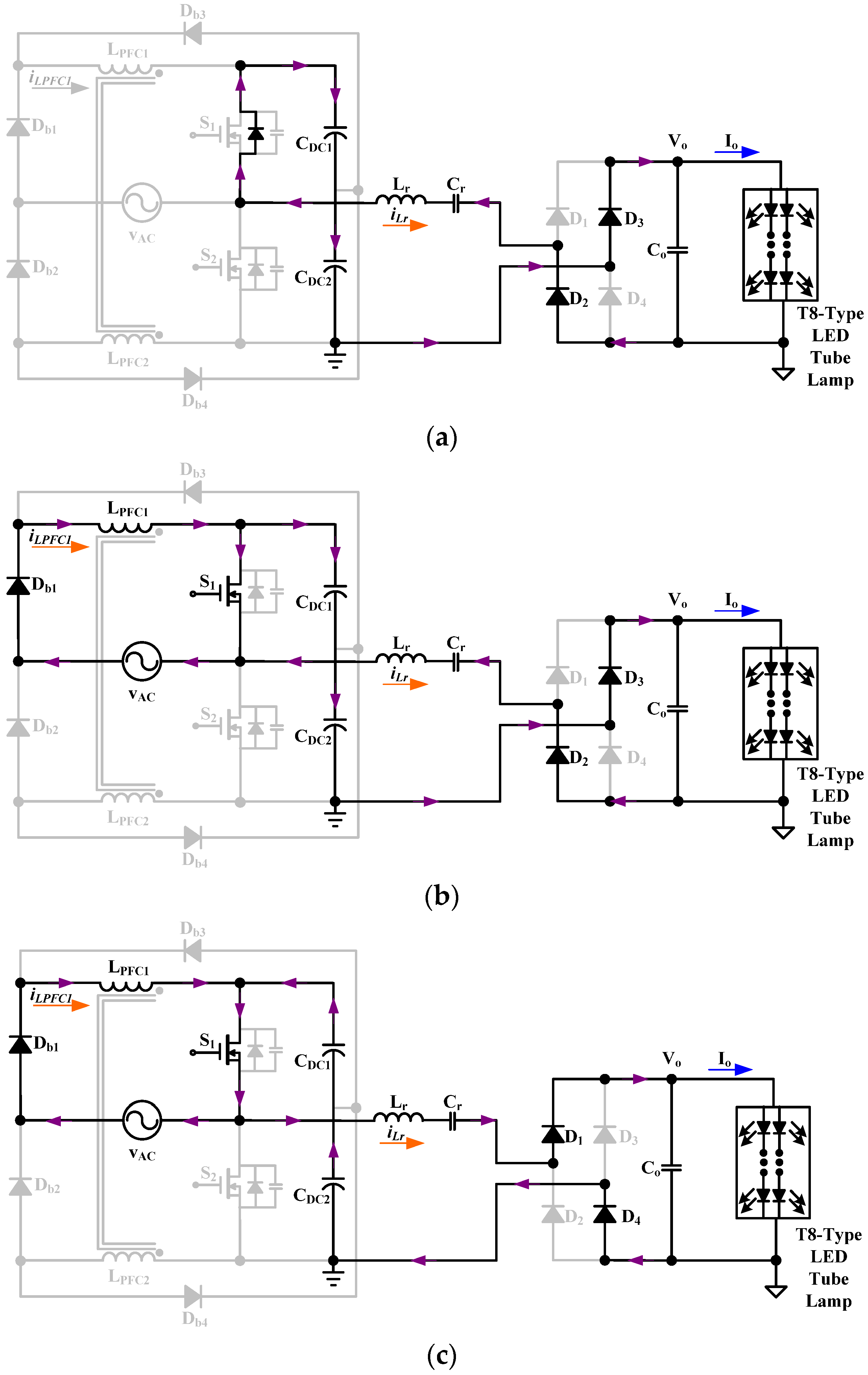
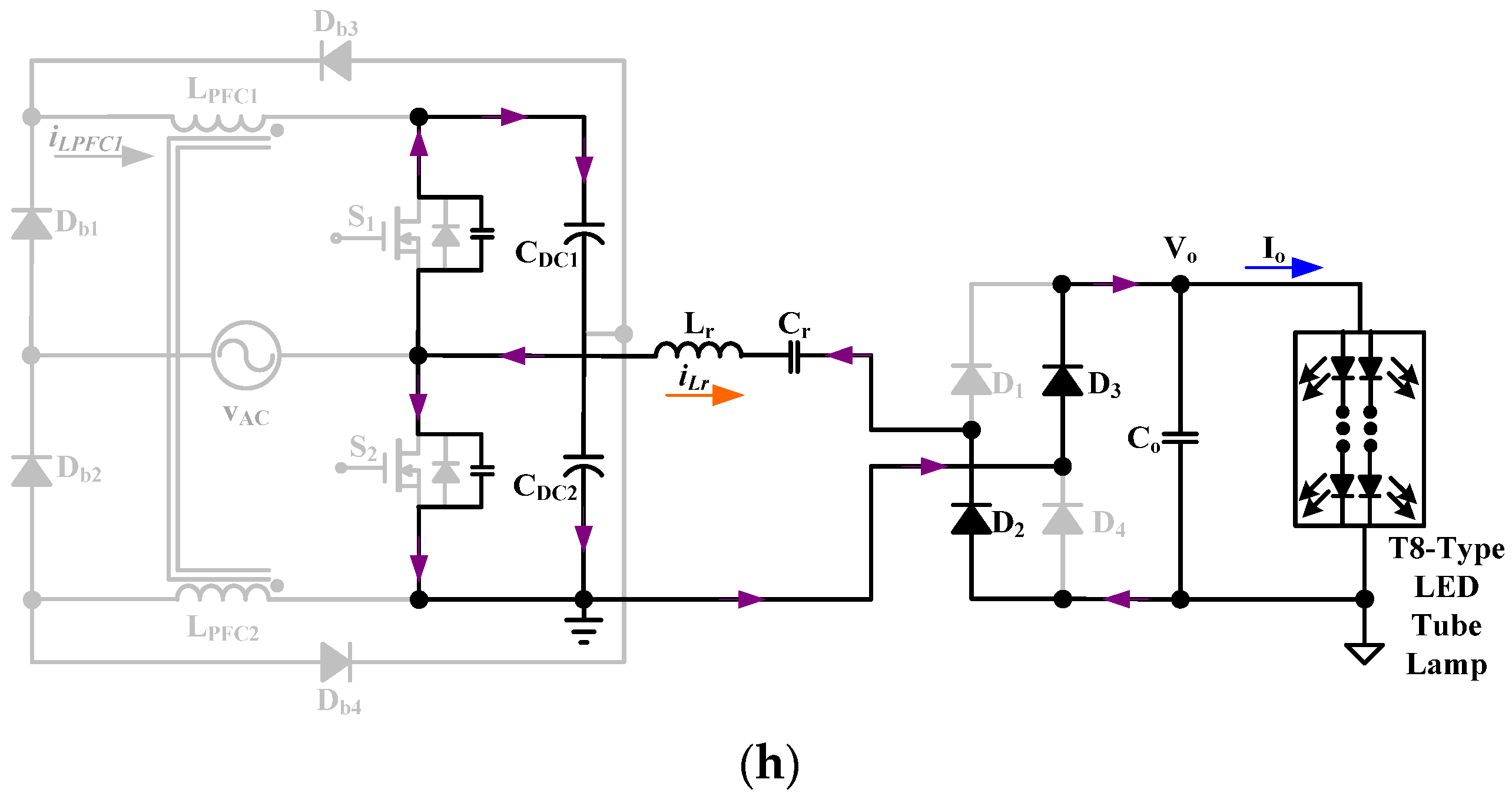
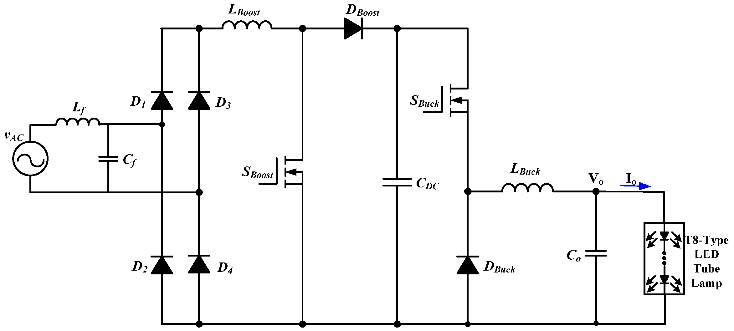
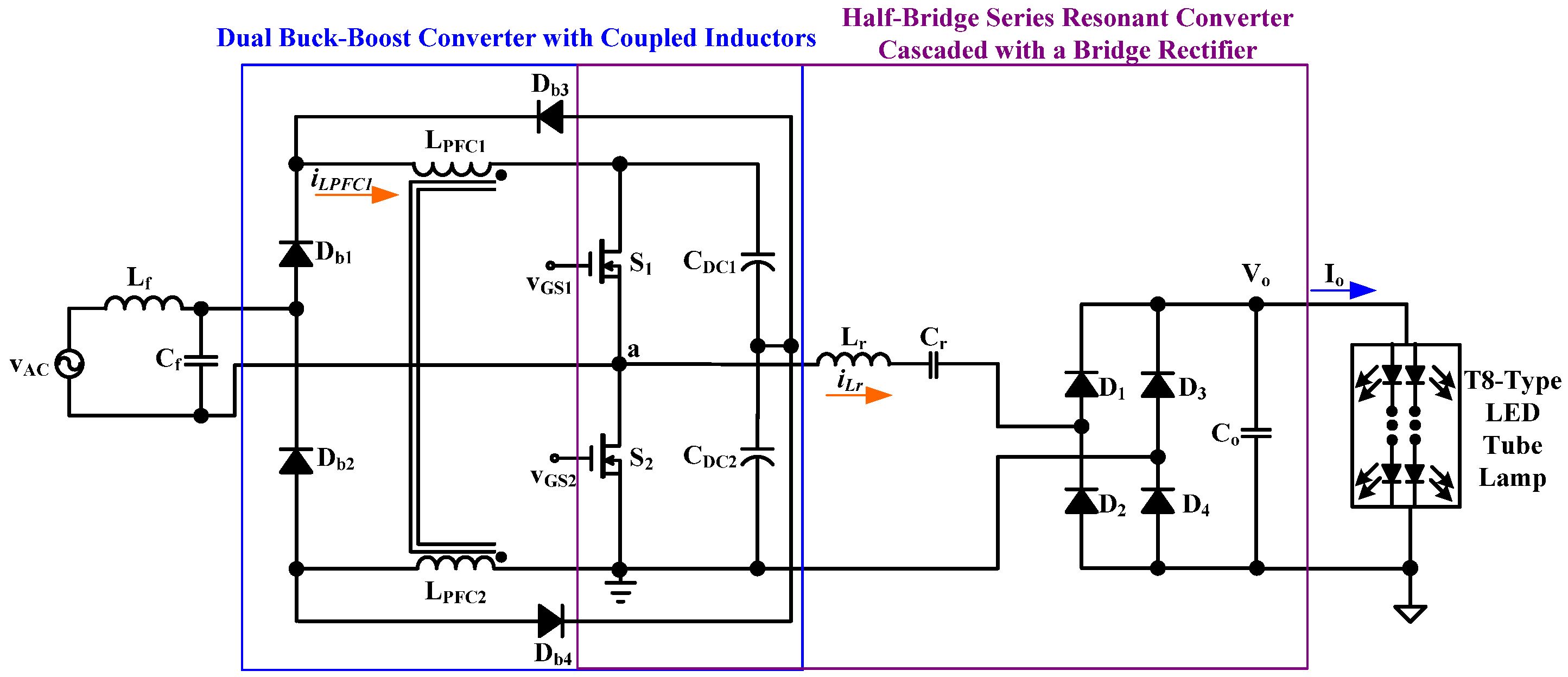
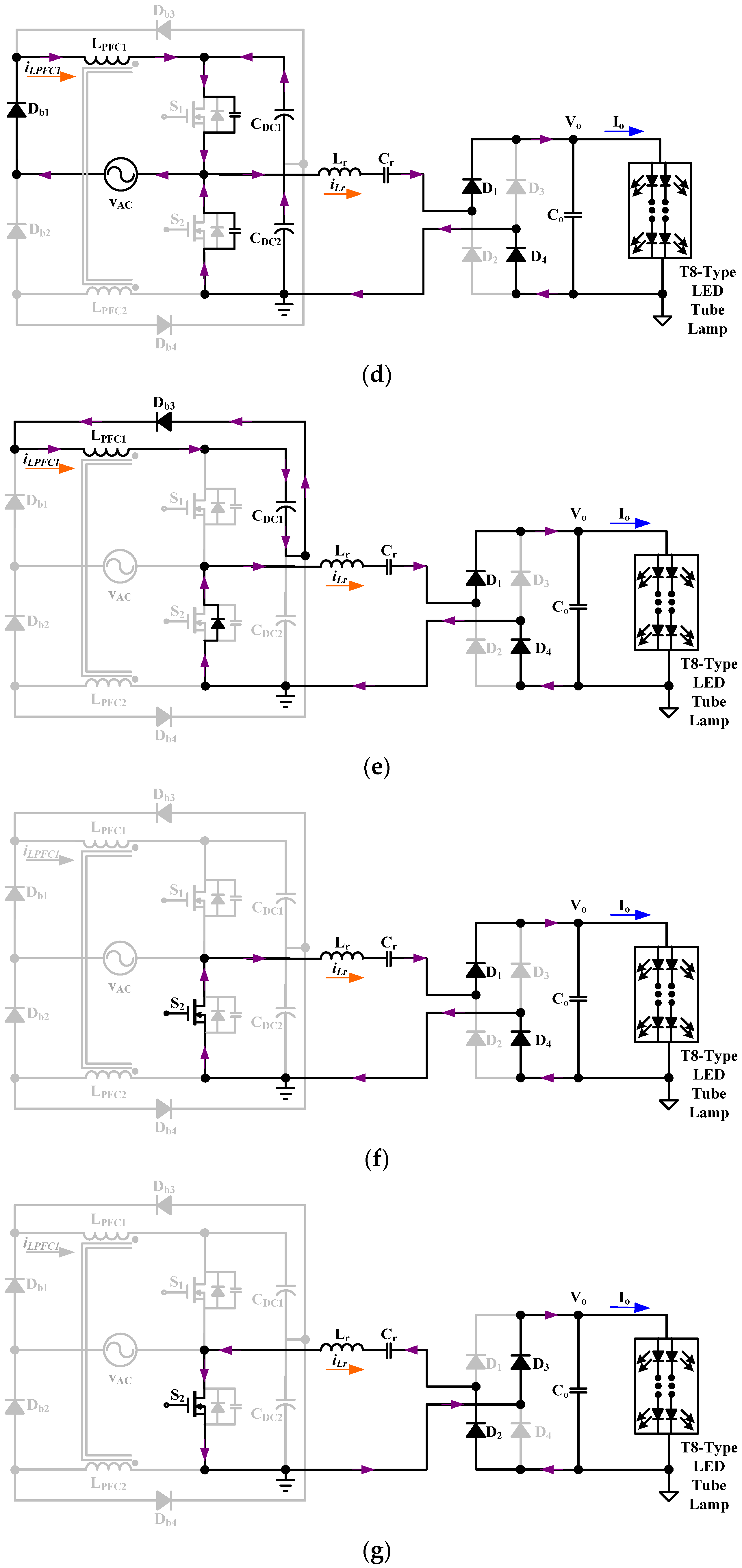
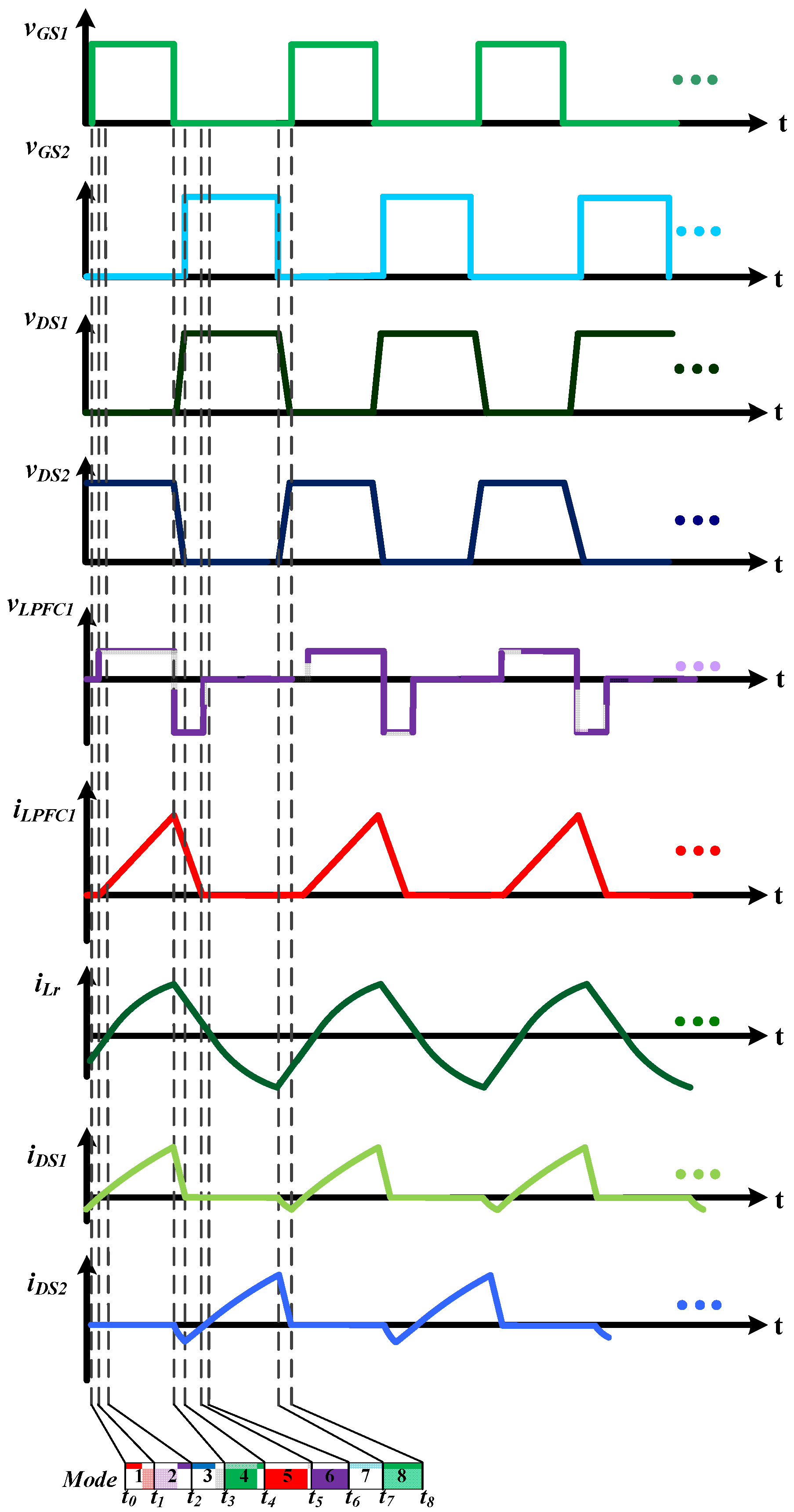
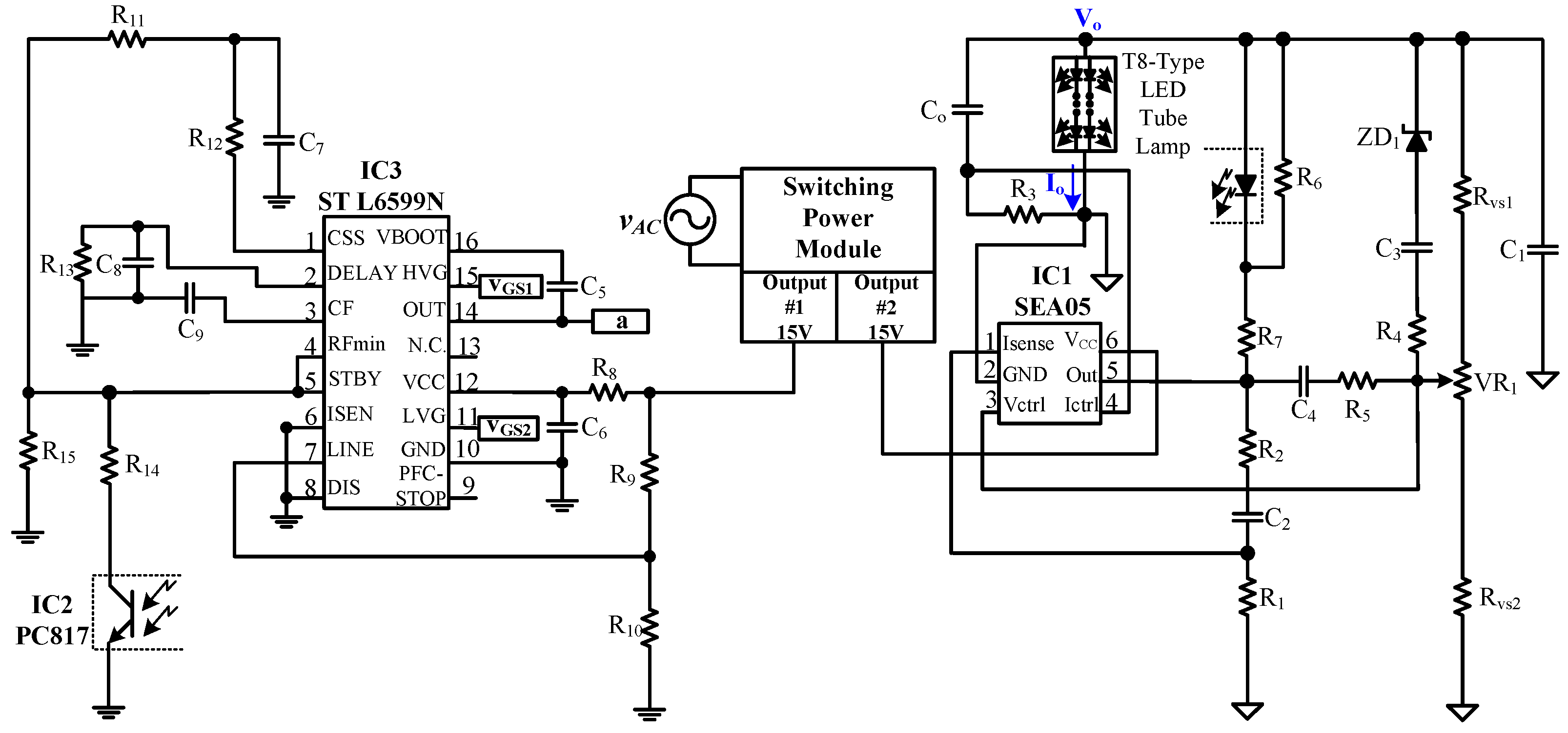
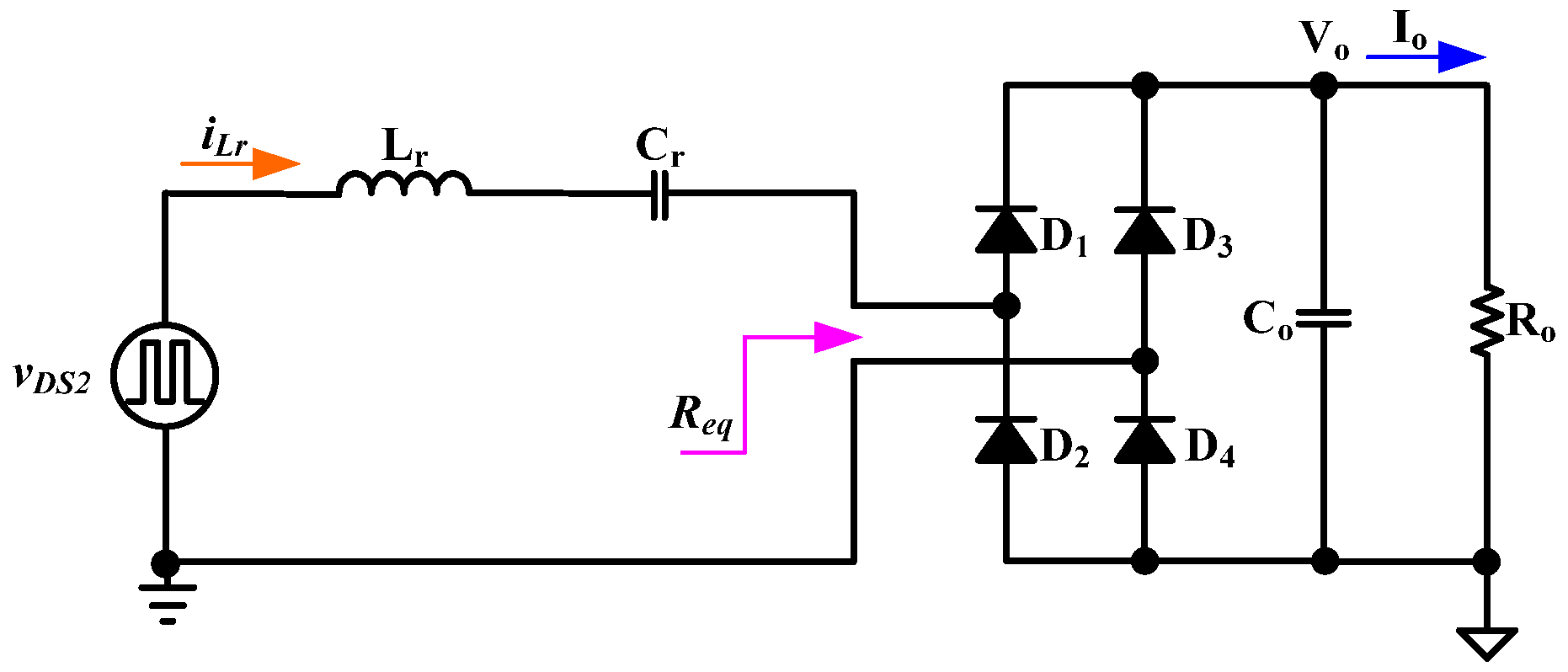
2. The Description and Analysis of the Presented LED Tube Lamp Driver

Figure 2 shows the presented driver, which integrates the dual buck-boost converter with coupled inductors (one buck-boost converter includes a diode Db1, a coupled inductor LPFC1, a switch S1, a body diode of the switch S2, and a DC-linked capacitor CDC1; another buck-boost converter includes a diode Db2, a coupled inductor LPFC2, a switch S2, a body diode of the switch S1, and the capacitor CDC2) with the half-bridge series resonant converter cascaded with a bridge rectifier (including two DC-linked capacitors CDC1 and CDC2, two switches S1 and S2, a resonant inductor Lr, a resonant capacitor Cr, a full-bridge rectifier (including diodes D1, D2, D3 and D4), and an output capacitor Co) into a single-stage topology for supplying an LED tube lamp [17]. In addition, an LC filter (an inductor Lf and a capacitor Cf) is connected with the input utility-line voltage.
In order to analyze the operations of the presented LED tube lamp driver, the following assumptions are made.
(a)
Since the switching frequencies of the two switches (S1 and S2) are much higher than that of the utility-line voltage vAC, the sinusoidal utility-line voltage can be considered as a constant value for each high-frequency switching period.
(b)
Power switches are complementarily operated, and their intrinsic diodes and inherent drain-source capacitors are considered.
(c)
The conducting voltage drops of all diodes (including Db1, Db2, Db3, Db4, D1, D2, D3 and D4) are neglected.
(d)
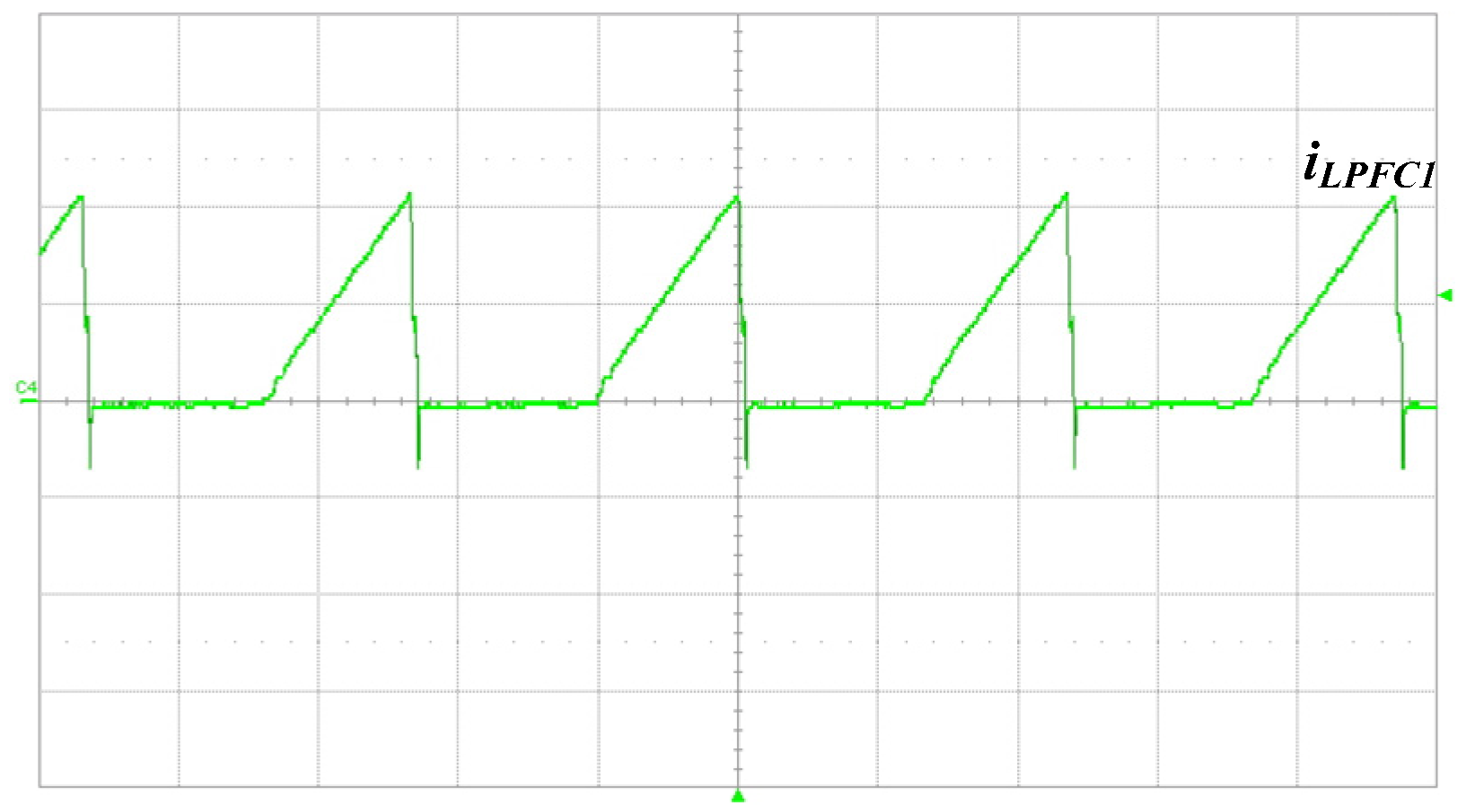
Two coupled inductors (LPFC1 and LPFC2) are designed to be operated in discontinuous-conduction mode (DCM) for naturally achieving power-factor correction (PFC).
The operating modes and key waveforms of the presented LED tube lamp driver during the positive half-cycle of input utility-line voltage are shown in Figure 3 and Figure 4, respectively, and the analysis of operations for the presented driver are described in detail as follows.
Mode 1 (t0t < t1; in Figure 3a): The drain-source voltage vDS1 of S1 is decreased to zero at time t0; thus, the body diode of switch S1 is forward-biased. The resonant capacitor Cr provides energy to resonant inductor Lr, capacitors CDC1, CDC2, Co and the LED tube lamp through S1’s body diode, D2, and D3. When power switch S1 turns on with zero-voltage switching (ZVS) at t1, this mode ends.
Mode 2 (t1t < t2; in Figure 3b): This mode begins when switch S1 achieves ZVS turn-on at t1. The input voltage vAC provides energy to coupled inductor LPFC1 through diode Db1 and switch S1. The inductor current iLPFC1 linearly increases from zero, and can be expressed as
i L P F C 1 ( t ) = 2 v A C r m s sin ( 2 π f A C t ) L P F C 1 ( t t 1 ) .
where vAC-rms is the root-mean-square (rms) value of the input utility-line voltage, and fAC is the utility-line frequency.
The resonant capacitor Cr still provides energy to inductor Lr, capacitors CDC1, CDC2, Co and the LED tube lamp through S1, D2, and D3. This mode finishes when the resonant inductor current iLr is zero at t2.
Mode 3 (t2t < t3; in Figure 3c): The input voltage vAC still provides energy to the coupled inductor LPFC1 through diode Db1 and switch S1. The DC-bus capacitors CDC1 and CDC2 supply energy to resonant inductor Lr, capacitors Cr and Co, and the LED tube lamp through switch S1, D1, and D4. This mode ends when inductor current iLPFC1 reaches its peak value at t3, which is denoted as iLPFC1-pk(t), and can be expressed as
i L P F C 1 p k ( t ) = 2 v A C r m s sin ( 2 π f A C t ) L P F C 1 D T S .
where D and TS are the duty cycle and period, respectively, of the power switch.
Mode 4 (t3t < t4; in Figure 3d): This mode begins when S1 turns off at t3. The utility-line voltage vAC and the coupled inductor LPFC1 supply energy to the drain-source capacitor of S1 through diode Db1.
The DC-bus capacitors CDC1 and CDC2, the drain-source capacitor of S2 and resonant inductor Lr provide energy to capacitors Cr and Co and the LED tube lamp through diodes D1 and D4. When the drain-source voltage vDS2 of S2 is decreased to zero at t4, this mode ends.
Mode 5 (t4t < t5; in Figure 3e): This mode begins when the body diode of switch S2 is forward-biased at t4. The coupled inductor LPFC1 provides energy to CDC1 through diode Db3. The inductor current iLPFC1 linearly decreases, and can be given by
i L P F C 1 ( t ) = 2 v A C r m s sin ( 2 π f A C t ) V D C / 2 L P F C 1 ( t t 4 ) .
where VDC/2 is the voltage of the DC-linked capacitor CDC1.
Inductor Lr provides energy to capacitors Cr and Co and the LED tube lamp through S2’s body diodes, D1 and D4. When power switch S2 is turned on with ZVS at t5, this mode ends.
Mode 6 (t5t < t6; in Figure 3f): This mode begins when switch S2 achieves ZVS turn-on at t5. Inductor Lr continues providing energy to capacitors Cr and Co and the LED tube lamp through S2, D1 and D4. The mode ends when the resonant inductor current iLr decreases to zero at t6.
Mode 7 (t6t < t7; in Figure 3g): This mode begins when current iLr decreases to zero at t6. Capacitor Cr provides energy to inductor Lr, capacitor Co and the LED tube lamp through S2 and diodes D2 and D3. The mode ends when switch S2 turns off at t7.
Mode 8 (t7t < t8; in Figure 3h): In this mode, capacitor Cr and the drain-source capacitor of switch S1 provide energy to inductor Lr, the drain-source capacitor of S2, capacitors CDC1, CDC2, Co, and the LED tube lamp through diodes D2 and D3. When the drain-source voltage vDS1 of S1 is decreased to zero at t7, this mode ends. Then, Mode 1 begins for the next high-frequency switching period.
Figure 5 shows the circuit diagram for controlling the single-stage LED tube lamp driver. Referring to Figure 5 and utilizing a constant voltage/current controller (IC1 SEA05) for regulating the LED tube lamp’s output voltage and current, the output voltage Vo can be sensed through resistors Rvs1, VR1 and Rvs2, and the output current can be sensed through resistor R3. The sensed output signal from pin 5 of the IC1 feeds into the high-voltage resonant controller (IC3 ST L6599) through a photo-coupler (IC2 PC817). Two gate-driving signals vGS1 and vGS2 are generated from pin 15 and pin 11, respectively, of the IC3, to carry out regulating the LED tube lamp’s output voltage and current. In addition, an AC-DC switching power module with dual output voltages is utilized for providing the 15 V power supply voltages of IC1 and IC3 in the control circuit.

3. Design Equations of Key Components in the Presented LED Tube Lamp Driver

3.1. Design of Coupled Inductors LPFC1 and LPFC2

The design equation of the coupled inductor LPFC1 (LPFC2) is expressed as [22]
L P F C 1 = η v A C r m s 2 D 2 2 P l a m p f S = L P F C 2
where η is the estimated circuit efficiency, Plamp is the rated power of the LED tube lamp, and fS is the switching frequency.
With a η of 0.9, a vAC-rms of 110 V and a Plamp of 18 W, an fS of 55 kHz and a D of 0.5, the coupled inductors LPFC1 and LPFC2 are given by:
L P F C 1 = L P F C 2 = 0.9 × 110 2 × 0.5 2 2 × 18 × 55,000 = 1.34 mH .

3.2. Design of Series Resonant Tank Lr and Cr

Figure 6 depicts the equivalent circuit during the design of the series resonant tank; Ro is the equivalent resistance of the T8-type LED tube lamp, and can be represented by Ro = Vo/Io. By using the fundamental approximation theory, the fundamental components of the switch voltage vDS2 can be expressed by [23,24]
v D S 2 f u n d = 2 π V D C sin 2 π f S t .
Referring to Figure 6, the equivalent load resistance Req can be expressed as [24]
R e q = 8 V o π 2 I o = 8 π 2 R o .
With a Vo of 60 V and an Io of 0.3 A, the equivalent load resistance Req is given by
R e q = 8 π 2 ( 60 0.3 ) = 162.1 Ω .
Referring to Figure 6, the series resonant tank is composed of a resonant inductor Lr in series connection with a resonant capacitor Cr; and the resonant frequency fo can be expressed by
f o = 1 2 π L r C r .
The loaded quality factor QL is expressed by
Q L = L r C r R e q .
In order to obtain ZVS for the two active switches, the switching frequency fS is designed to be larger than the resonant frequency fo so that the resonant tank resembles an inductive network [24].
Therefore, the relationship between switching frequency fS and resonant frequency fo is selected as
f S = 4 f o .
Combining (7) and (8) with (9), the resonant capacitor Cr is given by
C r = 2 π f S R e q Q L .
By selecting an fS of 55 kHz and a QL of 0.9, the resonant capacitor Cr is computed as
C r = 2 π × 55 k × 162.1 × 0.9 = 79.3 nF .
In addition, Cr is selected to be 82 nF.
Combining (7) with (9), the resonant inductor Lr is given by
L r = 4 π 2 f S 2 C r .
With an fS of 55 kHz and a Cr of 82 nF, the resonant inductor Lr is computed as
L r = 4 π 2 × ( 55 k ) 2 × 82 n = 1.63 mH .

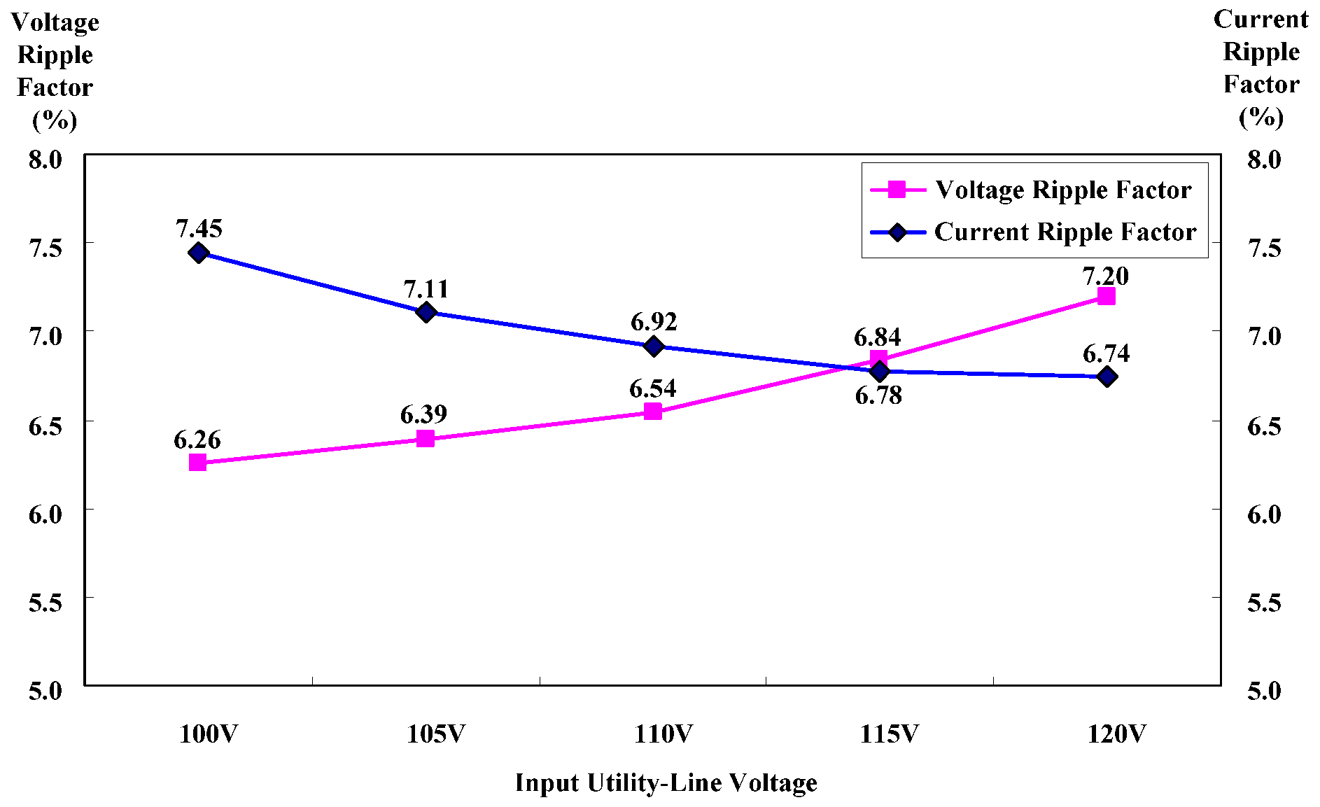
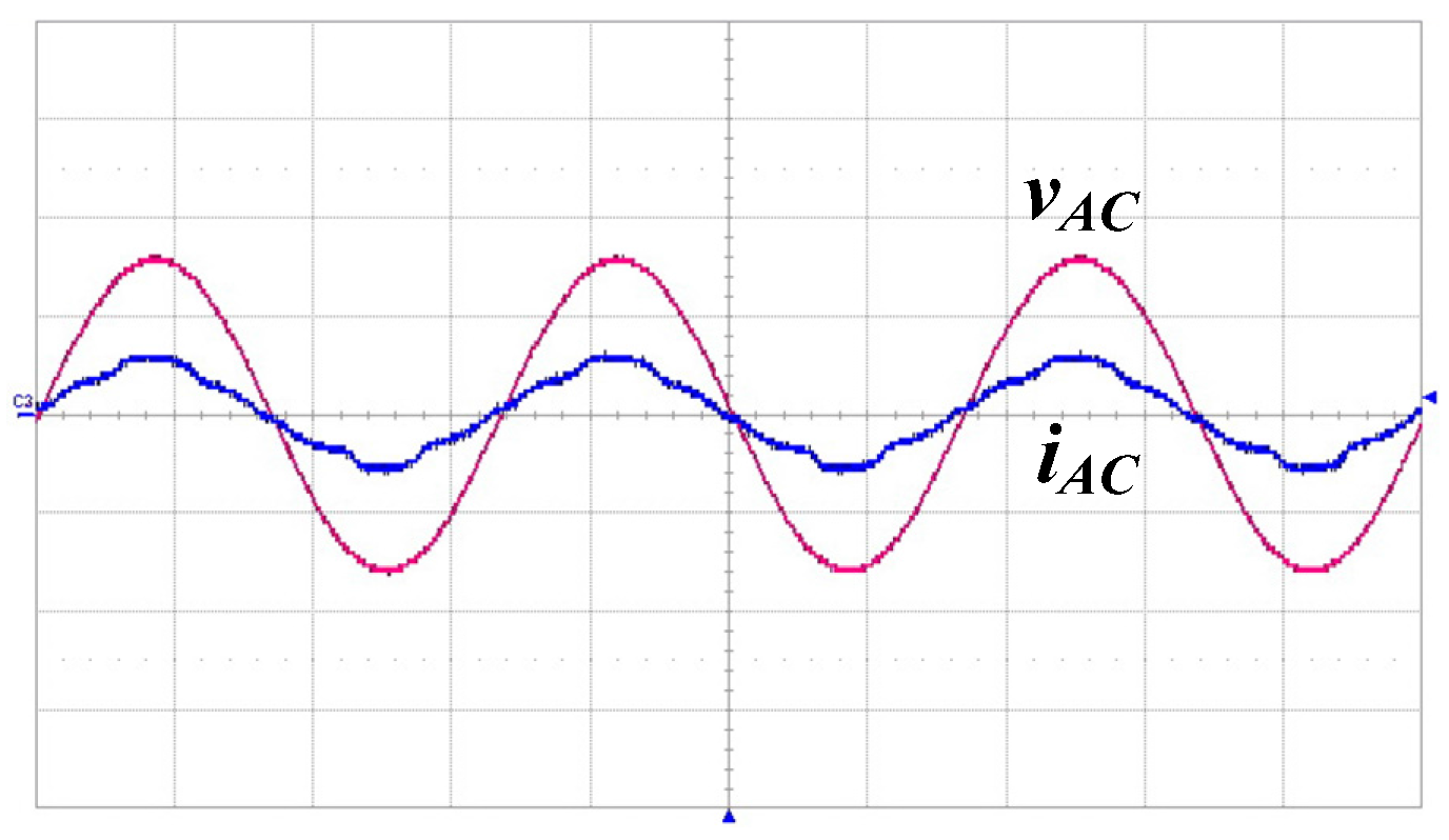
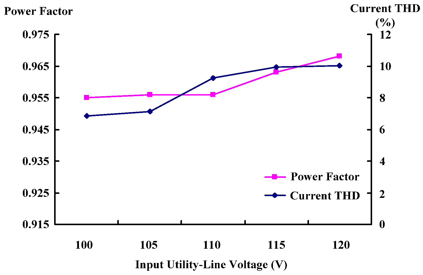
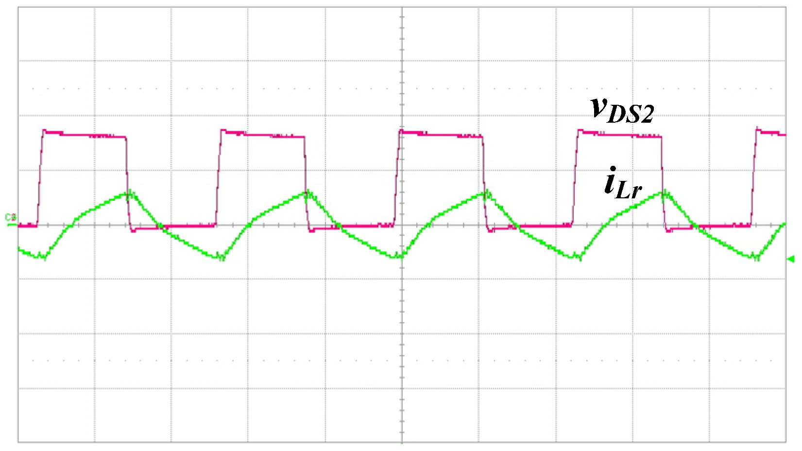
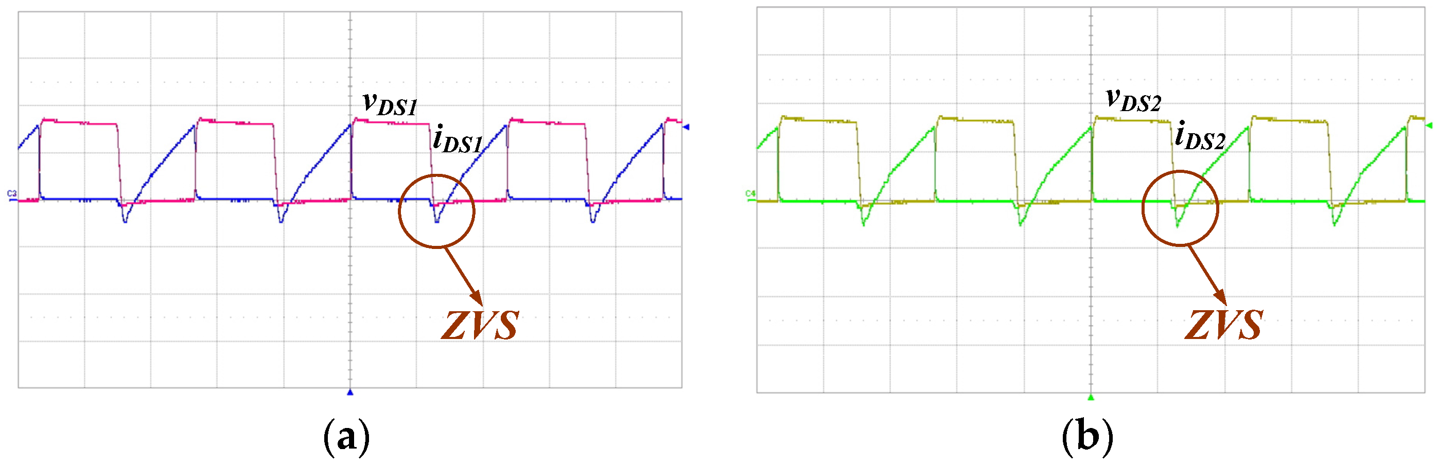
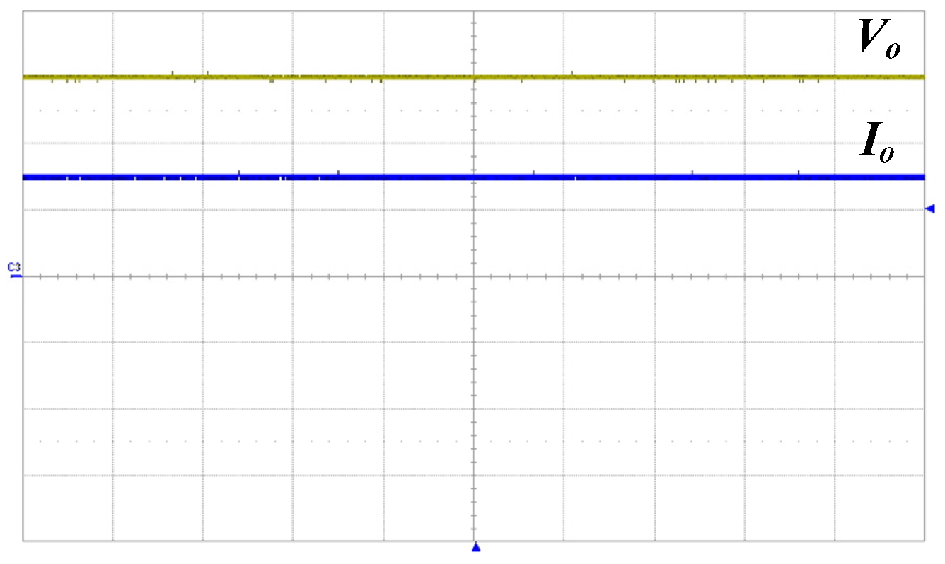
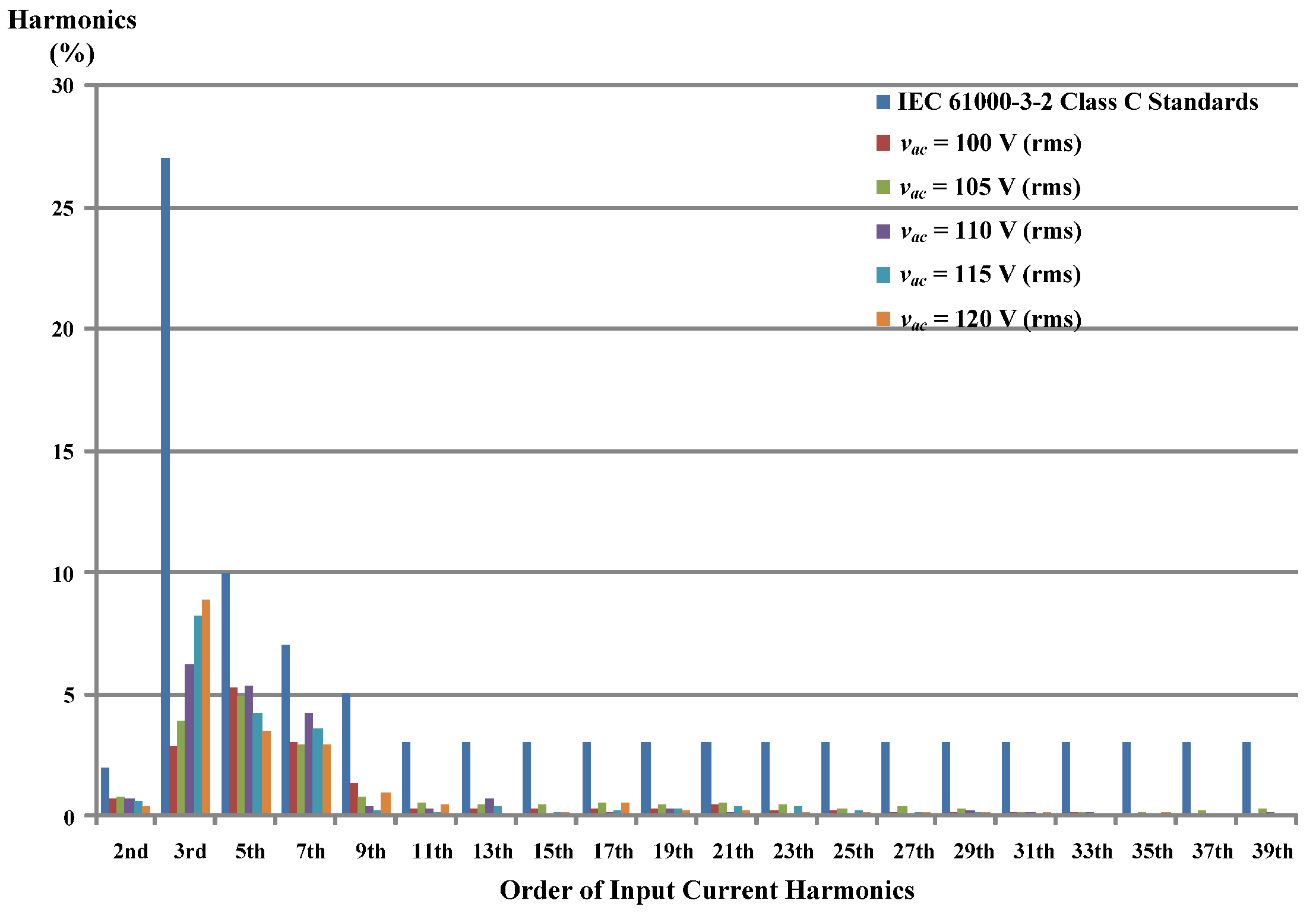
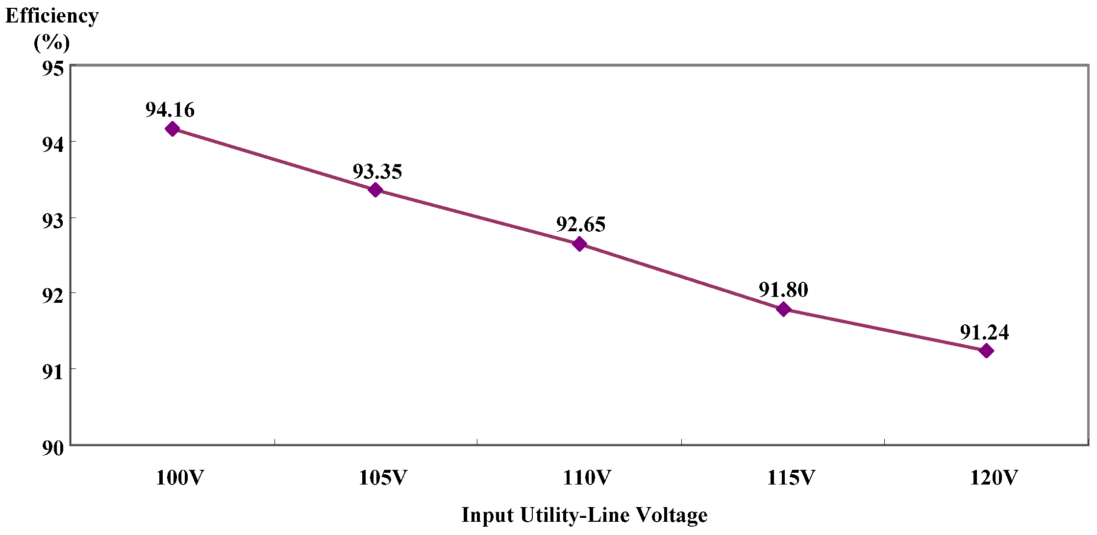
4. Experimental Results

A prototype driver has been built and tested for supplying an 18 W-rated T8-type LED tube lamp (EVERLIGHT FBW/T8/857/U/4ft, ELECTRONICS Co., Ltd., New Taipei City, Taiwan), whose rated voltage and current are 60 V and 0.3 A, respectively. The components utilized in the LED tube lamp driver are shown in Table 1.
Figure 7 presents the measured inductor current iLPFC1. The measured switch voltage vDS2 and inductor current iLr are shown in Figure 8, and the series resonant tank resembles an inductive load. The measured DC-bus voltage is shown in Figure 9, and the average value of VDC is approximately 318 V. Figure 10a,b presents the measured voltages vDS1 and vDS2 and currents iDS1 and iDS2 of the power switches S1 and S2, respectively. ZVS is obviously achieved on the power switches; thus, the circuit efficiency is increased.
Figure 11 shows the measured output voltage and current waveforms, and the average values of Vo and Io are 60 V and 0.3 A, respectively. Table 2 presents the measured output voltage and current of the presented LED tube lamp driver under different input voltages. Figure 12 shows the calculated voltage and current ripple factors of the presented LED tube lamp driver under different input utility-line voltages. In addition, the output voltage (current) ripple factor is obtained by the peak-to-peak (pk–pk) level divided by the average value of output voltage (current). According to Figure 12, the highest and lowest measured output-voltage ripple factors are 7.2% and 6.26%; these occurred at a utility-line rms voltage of 120 V and 100 V, respectively. Moreover, the highest and lowest measured output-current ripple factors are 7.45% and 6.74%; these occurred at a utility-line rms voltage of 100 V and 120 V, respectively.
The measured input utility-line voltage and current are shown in Figure 13, and the input current is in phase with the input voltage. Figure 14 presents the measured input-current harmonics compared with the International Electrotechnical Commission (IEC) 61000-3-2 Class C standards under input utility-line voltages ranging from 100 V to 120 V; all measured current harmonics meet the requirements. Figure 15 shows the measured power factor (PF) and current THD at input utility-line voltages ranging from 100 V to 120 V. At a utility-line rms voltage of 110 V, the measured PF and current THD are 0.96 and 9.3%, respectively. The maximum PF is 0.97 occurred at a utility-line rms voltage of 120 V, and the minimum current THD is 6.9% occurred at a utility-line rms voltage of 100 V.
Figure 16 shows the measured efficiency of the presented LED tube lamp driver under input utility-line voltages from 100 V to 120 V. The highest and lowest measured efficiency levels are 94.16% and 91.24%; these occurred at utility-line rms voltages of 100 V and 120 V, respectively. In addition, the efficiency which drops with increased utility-line voltages is related to the voltage gain of the LC series-resonant tank. For providing rated output power (voltage/current), the voltage gain of the LC series-resonant tank will decrease when the utility-line voltages increase, resulting in increasing the switching frequency of the power switches. Thus, the switching losses of power switches and conduction losses of power diodes will increase resulting in lowering the circuit efficiency.
The comparisons between the existing T8-Type LED tube lamp drivers and the proposed one are shown in Table 3. A flyback-type AC-DC converter as an LED tube lamp driver is presented in [18], and a buck-type AC-DC converter as an LED tube lamp driver is presented in [19]. In addition, these existing LED tube lamp drivers ([18,19]) operate with universal input voltages while the proposed version operates with American utility-line voltages. Although the circuit components counts in the proposed driver are higher than these existing ones, this table illustrates that the proposed single-stage LED tube lamp driver has smaller input current THD and achieves soft-switching on the power switches to increase circuit efficiency over the two existing versions.

5. Conclusions

This paper has presented and implemented a single-stage driver suitable for energy-saving indoor lighting applications, which integrates a dual buck-boost converter with coupled inductors and a half-bridge series resonant converter cascaded with a bridge rectifier, for supplying an LED tube lamp for T8/T10 fluorescent lamp replacements with power-factor corrections and soft switching. A prototype circuit has been successfully built and tested for supplying an 18 W-rated LED tube lamp with utility-line voltages ranging from 100 V to 120 V. The experimental results have demonstrated high efficiency (>91%), satisfying power-factor (>0.96), low current THD (<10%), and soft-switching of power switches in the presented LED tube lamp driver.

Acknowledgments

The authors would like to convey their appreciation for grant support from the Ministry of Science and Technology (MOST) of Taiwan under its grant with reference number MOST 103-2221-E-214-024.

Author Contributions

Chun-An Cheng conceived and designed the circuit. En-Chih Chang performed circuit simulations. Ching-Hsien Tseng and Tsung-Yuan Chung carried out the prototype driver, and measured as well as analyzed experimental results with the guidance from Chun-An Cheng. En-Chih Chang revised the manuscript for submission.

Conflicts of Interest

The authors declare no conflict of interest.

References

  1. Bender, V.C.; Marchesan, T.B.; Alonso, J.M. Solid-state lighting: A concise review of the state of the art on LED and OLED modeling. IEEE Ind. Electron. Mag. 2015, 9, 6–16. [Google Scholar] [CrossRef]
  2. Brañas, C.; Azcondo, F.J.; Alonso, J.M. Solid-state lighting: A system review. IEEE Ind. Electron. Mag. 2013, 7, 6–14. [Google Scholar] [CrossRef]
  3. Liang, T.J.; Tseng, W.J.; Chen, J.F.; Wu, J.P. A novel line frequency multistage conduction LED driver with high power factor. IEEE Trans. Power Electron. 2015, 30, 5103–5115. [Google Scholar] [CrossRef]
  4. Moo, C.S.; Chen, Y.J.; Yang, W.C. An efficient driver for dimmable LED lighting. IEEE Trans. Power Electron. 2012, 27, 4613–4618. [Google Scholar] [CrossRef]
  5. Wang, Y.; Guan, Y.; Ren, K.; Xu, D. A single-stage LED driver based on BCM boost circuit and converter for street lighting system. IEEE Trans. Ind. Electron. 2015, 62, 5446–5457. [Google Scholar] [CrossRef]
  6. Kwak, S.S. Pulse-driven LED circuit with transformer-based current balance technique. Int. J. Electron. 2014, 101, 1683–1693. [Google Scholar] [CrossRef]
  7. Hsia, S.C.; Sheu, M.H.; Lai, S.Y. Chip implementation of high-efficient light-emitting diode dimming driver for high-power light-emitting diode lighting system. IET Power Electron. 2015, 8, 1043–1051. [Google Scholar] [CrossRef]
  8. Choi, W.Y.; Yang, M.K. High-efficiency isolated SEPIC converter with reduced conduction losses for LED displays. Int. J. Electron. 2014, 101, 1495–1502. [Google Scholar] [CrossRef]
  9. Chen, Y.S.; Liang, T.J.; Chen, K.H.; Juang, J.N. Study and implementation of high frequency pulse LED driver with self-oscillating circuit. In Proceedings of the IEEE International Symposium on Circuit and Systems (ISCAS), Rio de Janeiro, Brazil, 15–18 May 2011; pp. 498–501.
  10. Wang, Y.; Guan, Y.; Zhang, X.; Xu, D. Single-stage LED driver with low bus voltage. Eletron. Lett. 2013, 49, 455–456. [Google Scholar] [CrossRef]
  11. Hui, S.Y.R.; Li, S.N.; Tao, X.H.; Chen, W.; Ng, W.M. A novel passive off-line light-emitting diode (LED) driver with long lifetime. IEEE Trans. Power Electron. 2010, 25, 2665–2672. [Google Scholar] [CrossRef]
  12. Qu, X.; Wong, S.C.; Tse, C.K. Resonance-assisted buck converter for offline driving of power LED replacement lamps. IEEE Trans. Power Electron. 2011, 26, 532–540. [Google Scholar]
  13. Wang, Y.; Guan, Y.; Huang, J.; Wang, W.; Xu, D. A single-stage LED driver based on interleaved buck-boost circuit and LLC resonant converter. IEEE J. Emerg. Sel. Top. Power Electron. 2015, 3, 732–741. [Google Scholar] [CrossRef]
  14. Chang, Y.N.; Kuo, C.M.; Cheng, H.L.; Lee, C.R. Design of dimmable LED lighting driving circuit for battery power source. In Proceedings of the 10th IEEE International Conference on Power Electronics and Drive Systems (PEDS), Kitakyushu, Japan, 22–25 April 2013; pp. 1168–1172.
  15. Lin, C.C.; Yang, L.S.; Chang, E.C. Study of a DC-DC converter for solar LED street lighting. In Proceedings of the IEEE International Symposium on Next-Generation Electronics (ISNE), Kaohsiung, Taiwan, 25–26 February 2013; pp. 461–464.
  16. Chen, N.; Chung, H.S.H. A driving technology for retrofit LED lamp for fluorescent lighting fixtures with electronic ballasts. IEEE Trans. Power Electron. 2011, 26, 588–601. [Google Scholar] [CrossRef]
  17. Cheng, C.A.; Chang, E.C.; Tseng, C.S.; Chung, T.Y. A novel single-stage LED driver with coupled inductors and interleaved PFC. In Proceedings of the International Symposium on Computer, Consumer and Control, Taichung, Taiwan, 10–12 June 2014; pp. 1287–1290.
  18. Texas Instruments. 19 W, Single-Stage AC/DC LED Driver for T8/T10 Fluorescent Lamp Replacement; Texas Instruments: Dallas, TX, USA, 2011; pp. 1–21. [Google Scholar]
  19. Fairchild Semiconductor. User Guide for FEBFL7701 L34U018A Evaluation Board Universal Input 18.3 W LED Driver; Fairchild Semiconductor: Sunnyvale, CA, USA, 2012; pp. 1–24. [Google Scholar]
  20. Catalog of Lamps. China Electric MFG. Corporation. Available online: http://ebook.chinaelectric.com.tw/hosts/2/7/files/2712651479460151/book.php (accessed on 9 August2016).
  21. Catalog of LED Lamps. Everlight Electronics Co., Ltd. Available online: http://www.everlightlighting.com/file/image/files/ELL_2015_Catalogue_dealer.pdf (accessed on 18 May 2015).
  22. Cheng, C.A.; Cheng, H.L.; Chung, T.Y. A novel single-stage high-power-factor LED street-lighting driver with coupled inductors. IEEE Trans. Ind. Appl. 2014, 50, 3037–3045. [Google Scholar] [CrossRef]
  23. Steigerwald, R.L. A comparison of half-bridge resonant converter topology. IEEE Trans. Power Electron. 1988, 3, 174–182. [Google Scholar] [CrossRef]
  24. Kazimierczuk, M.K.; Czarkowski, D. Resonant Power Converters; Wiley: New York, NY, USA, 1995. [Google Scholar]
Figure 1. The commercial two-stage driver for supplying a T8-Type LED (light-emitting diode) tube lamp.
Applsci 07 00115 g001
Figure 2. The presented single-stage driver for supplying a T8-type LED tube lamp.
Applsci 07 00115 g002
Figure 3. Operation modes of the presented driver during the positive half-cycle of input voltage vAC. (a) Mode 1; (b) Mode 2; (c) Mode 3; (d) Mode 4; (e) Mode 5; (f) Mode 6; (g) Mode 7; (h) Mode 8.
Applsci 07 00115 g003aApplsci 07 00115 g003bApplsci 07 00115 g003c
Figure 4. Key waveforms of the presented LED tube lamp driver during the positive half-cycle of the input utility-line voltage.
Applsci 07 00115 g004
Figure 5. The utilized control circuit for the presented LED tube lamp driver.
Applsci 07 00115 g005
Figure 6. Equivalent circuit during the design of the series resonant tank.
Applsci 07 00115 g006
Figure 7. Measured inductor current iLPFC1 (0.5 A/div); time scale: 5 μs/div.
Applsci 07 00115 g007
Figure 8. Measured voltage vDS2 (200 V/div) and inductor current iLr (1 A/div); time scale: 5 μs/div.
Applsci 07 00115 g008
Figure 9. Measured DC (direct current)-bus voltage VDC occurred on DC-linked capacitors (CDC1 and CDC2) (100 V/div); time scale: 5 μs/div.
Applsci 07 00115 g009
Figure 10. (a) Measured voltage vDS1 (200 V/div) and current iDS1 (1 A/div); time scale: 5 μs/div; (b) Measured voltage vDS2 (200 V/div) and current iDS2 (1 A/div); time scale: 5 μs/div.
Applsci 07 00115 g010
Figure 11. Measured output voltage Vo (20 V/div) and current Io (0.2 A/div); time scale: 2 ms/div.
Applsci 07 00115 g011
Figure 12. Calculated voltage and current ripple factors of the presented LED tube lamp driver under different input utility-line voltages.
Applsci 07 00115 g012
Figure 13. Measured input utility-line voltage vAC (100 V/div) and current iAC (0.5 A/div); time scale: 5 ms/div.
Applsci 07 00115 g013
Figure 14. Measured input-current harmonics compared with the IEC 61000-3-2 Class C standards.
Applsci 07 00115 g014
Figure 15. Measured power factor and current total-harmonic distortion (THD) of the presented LED tube lamp driver under different input utility-line voltages.
Applsci 07 00115 g015
Figure 16. Measured efficiency of the presented LED tube lamp driver under different input utility-line voltages.
Applsci 07 00115 g016
Table 1. Key components used in the presented led tube lamp driver.
ComponentValue
Filter Inductor (Lf)2 mH
Filter Capacitor (Cf)0.68 μF/250 V
Diodes (Db1, Db2)MUR460
Power Switches (S1, S2)IRF840
Coupled Inductors (LPFC1, LPFC2)1.34 mH
DC (direct current)-Linked Capacitors (CDC1, CDC2)100 μF/450 V
Resonant Inductor (Lr)1.68 mH
Resonant Capacitor (Cr)82 nF
Diodes (D1, D2, D3, D4)MUR460
Output Capacitor (Co)200 μF/63 V
Table 2. Measured output voltage and current of the presented led tube lamp driver under different input voltages.
Input Voltage100 V105 V110 V115 V120 V
Parameters
Output Voltage (mean)60.07 V60.1 V60.08 V60.11 V60.16 V
Output Voltage (pk–pk)3.76 V3.84 V3.93 V4.11 V4.33 V
Output Current (mean)0.321 A0.311 A0.308 A0.304 A0.301 A
Output Current (pk–pk)23.9 mA22.1 mA21.3 mA20.6 mA20.3 mA
Table 3. Comparisons between the existing t8-type led tube lamp drivers and the proposed one.
ItemExisting LED (Direct Current) Tube Lamp Driver in [18]Existing LED Tube Lamp Driver in [19]Proposed LED Tube Lamp Driver
Circuit TopologyFlyback-type AC-DC (alternating current-direct current) ConverterBuck-type AC-DC ConverterIntegration of a Dual Buck-Boost Converter with coupled inductors and a Half-Bridge Series Resonant Converter cascaded with a bridge rectifier
Input Utility-Line Voltages90~264 V90~264 V100~120 V
Rated Output Power (Rated Output Voltage/Current)19 W (42 V/0.45 A)18.3 W (39 V/0.47 A)18 W (60 V/0.3 A)
Required Power Switch1 (Without Soft-Switching)1 (Without Soft-Switching)2 (With Soft-Switching)
Measured Maximum Power Factor0.99 @ 110 V0.96 @ 110 V0.97 @ 120 V
Measured Minimum Input Current THD (total-harmonic distortion)9% @ 180 V21.54% @ 110 V6.86% @ 100 V
Measured Maximum Efficiency87.8% @ 180 V88.56% @ 180 V94.16% @ 100 V

