
Optimization of Silicon MZM Fabrication Parameters for High Speed Short Reach Interconnects at 1310 nm

Abstract
:1. Introduction
2. Notations and Methodology
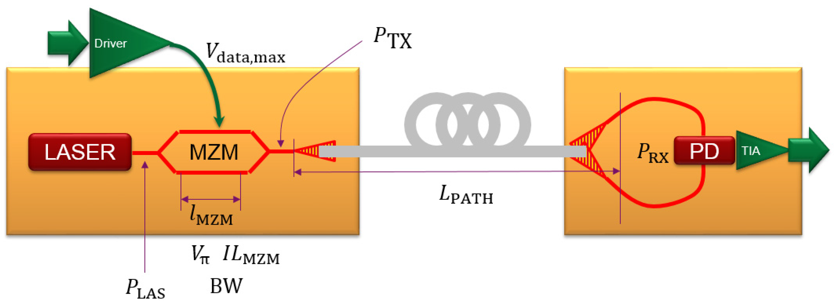
2.1. Presentation of a Typical High Speed Short Reach Interconnect
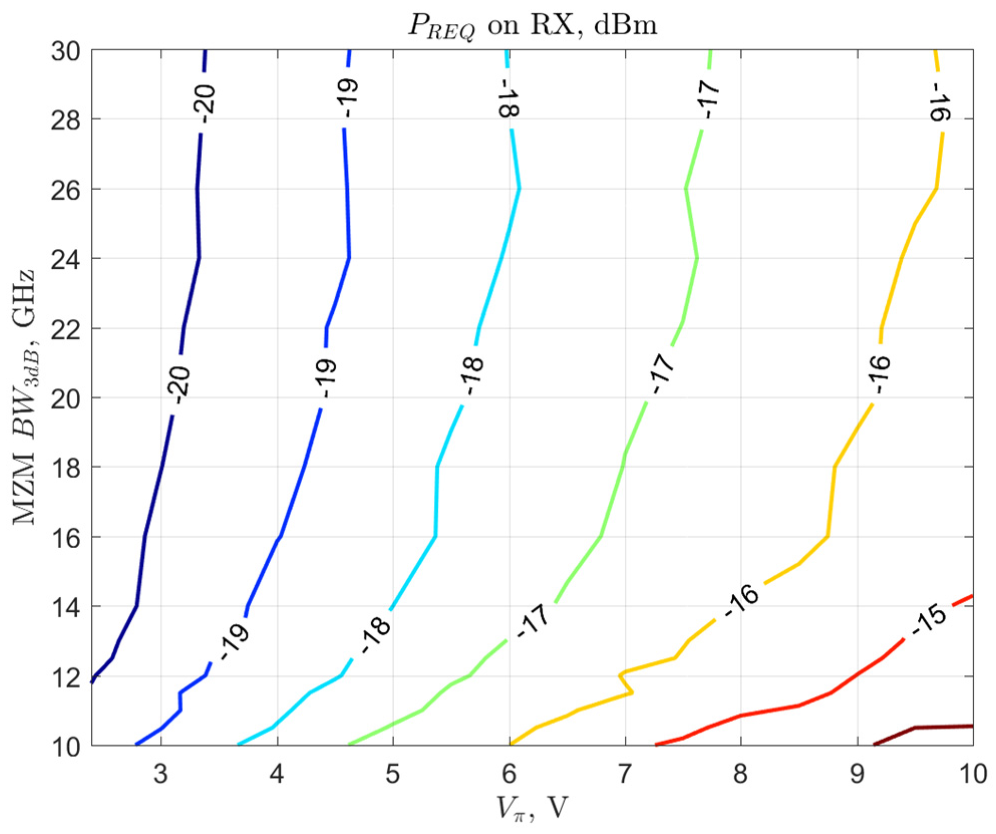
2.2. Simulation of the Input Power Required
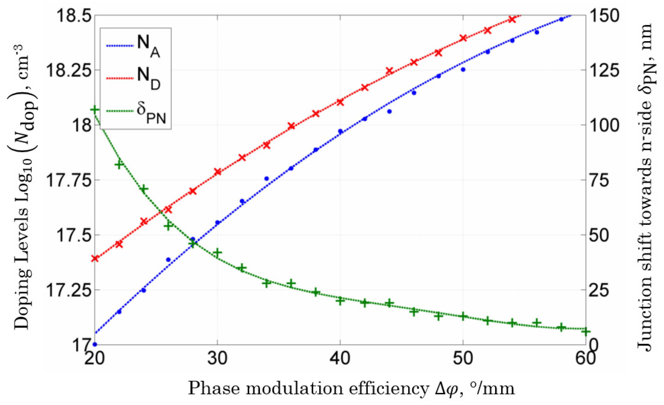
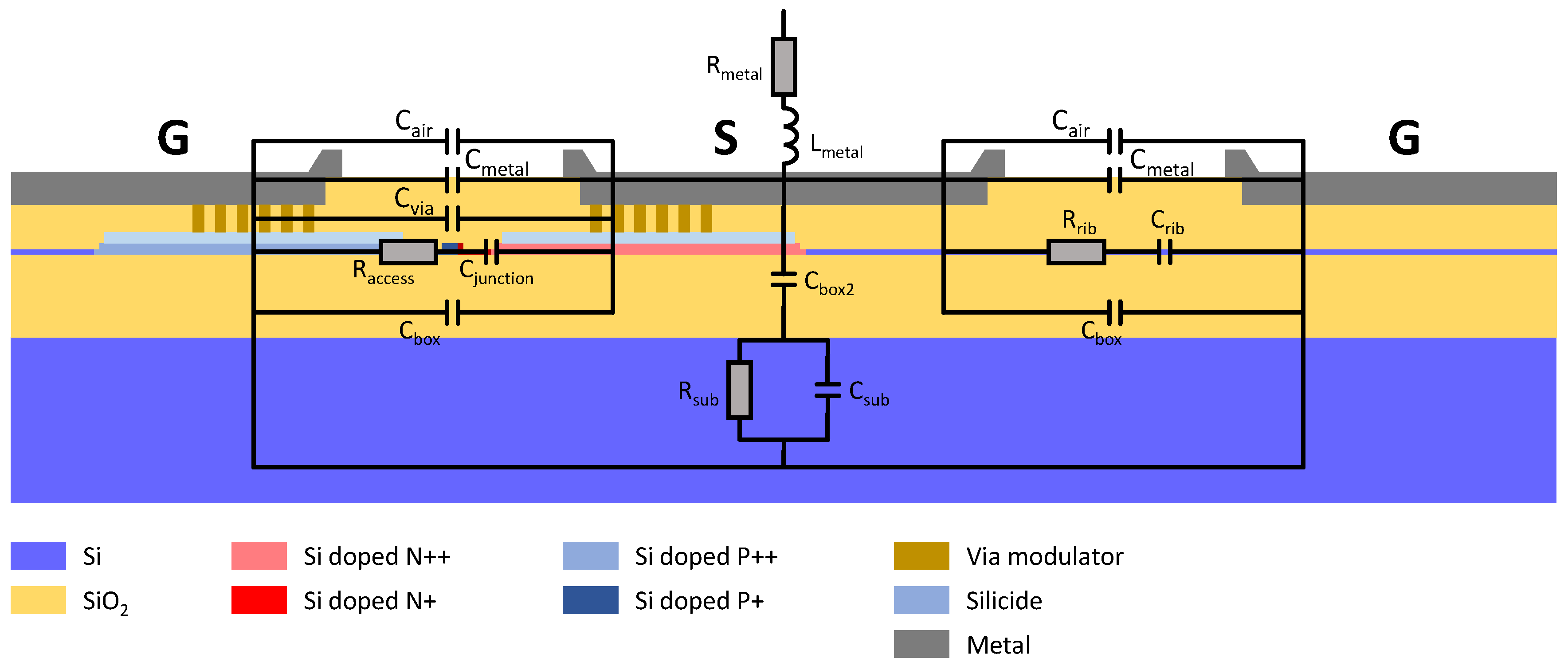
2.3. EO Performances of the Active Region of the MZM
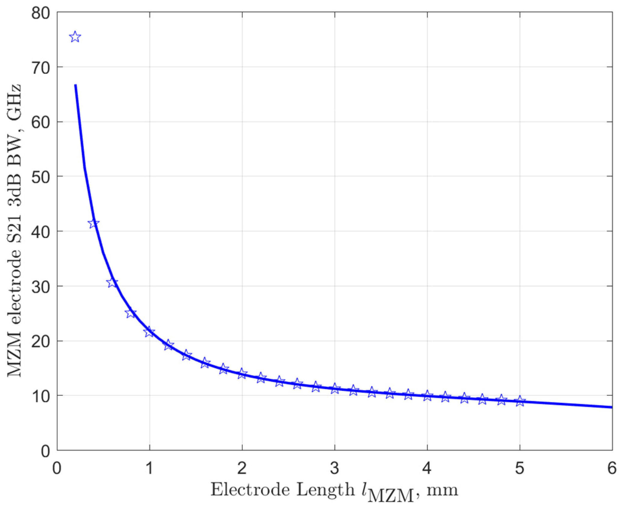
2.4. Modulation Bandwidth
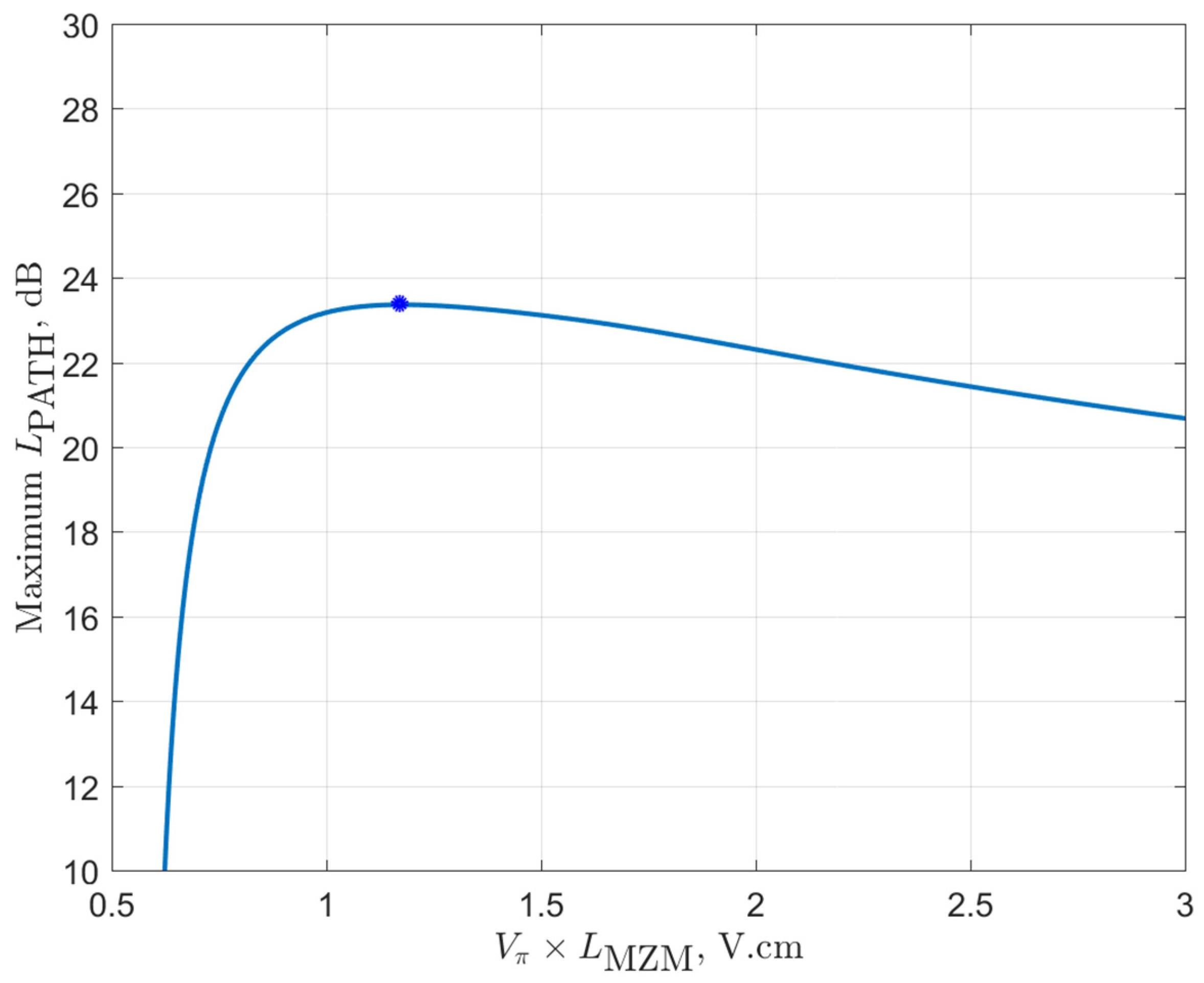
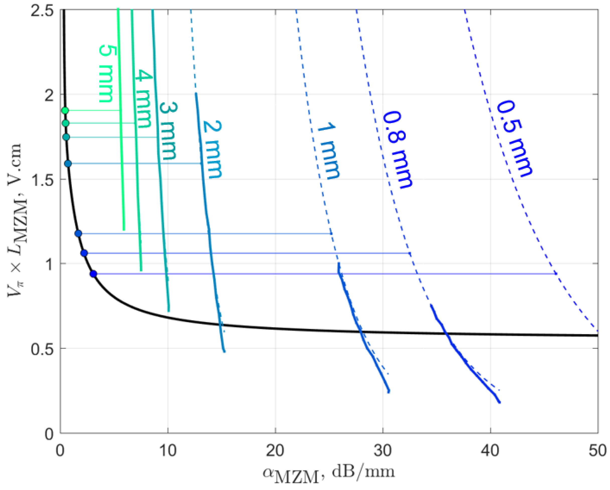
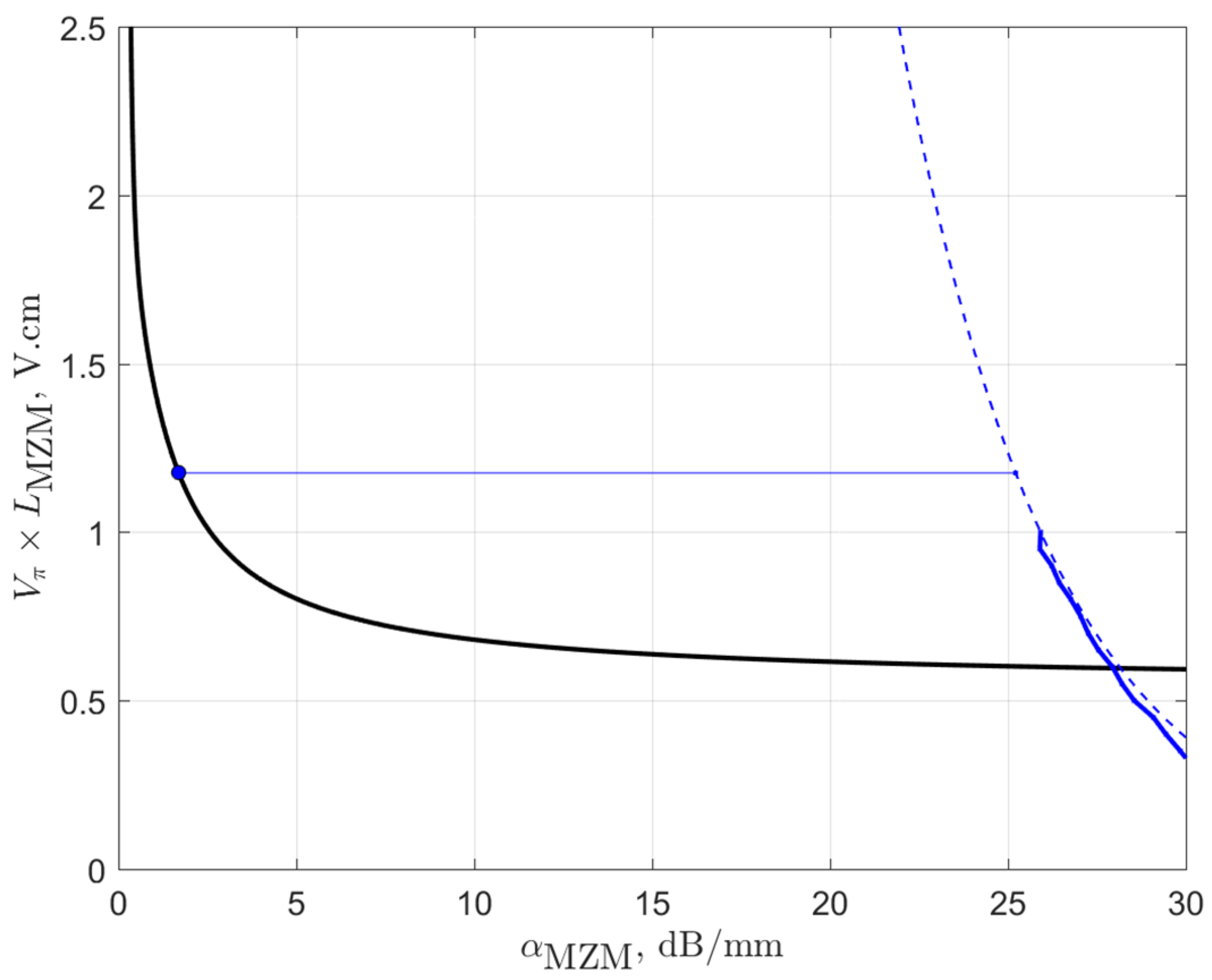
3. MZM Parameter Optimization
4. Conclusions
Acknowledgments
Author Contributions
Conflicts of Interest
References
- Bernabe, S.; Charbonnier, B.; Blampey, B.; Malhouitre, S.; Castany, O.; Temporiti, E.; Minoia, G.; Baldi, G.; Repossi, M.; Pares, G.; et al. A fully packaged 25 Gbps/channel WDM photoreceiver module based on a Silicon Photonic Integrated Circuit and a flip-chipped CMOS quad Transimpedance Amplifier. In Proceedings of the IEEE Optical Interconnects Conference (OI), San Diego, CA, USA, 9–11 May 2016.
- Sun, C.; Wade, M.T.; Lee, Y.; Orcutt, J.S.; Alloatti, L.; Georgas, M.S.; Waterman, A.S.; Shainline, J.M.; Avizienis, R.R.; Lin, S.; et al. Single-chip microprocessor that communicates directly using light. Nature 2015, 528, 534–538. [Google Scholar] [CrossRef] [PubMed]
- Milivojevic, B.; Wiese, S.; Anderson, S.; Brenner, T.; Webster, M. Demonstration of Optical Transmission at Bit Rates of up to 321.4 Gb/s using Compact Silicon Based Modulator and Linear BiCMOS MZM Driver. In Proceedings of the Optical Fiber Communications Conference, Anaheim, CA, USA, 20–24 March 2016.
- Temporiti, E.; Minoia, G.; Repossi, M.; Baldi, D.; Ghilioni, A.; Svelto, F. A 56 Gbps 300 mW Silicon-Photonics Transmitter in 3D-Integrated PIC25G and 55 nm BiCMOS Technologies. In Proceedings of the International Solid-State Circuit Conference (ISSCC), San Francisco, CA, USA, 31 January–4 February 2016.
- Thomson, D.; Zilkie, A.; Bowers, J.; Komljenovic, T.; Reed, G.; Vivien, L.; Marris-Morini, D.; Cassan, E.; Virot, L.; Fédéli, J.M.; et al. Roadmap on silicon photonics. J. Opt. 2016, 18. [Google Scholar] [CrossRef]
- Mellanox MFS1200-xxxx. Available online: www.mellanox.com (accessed on 19 October 2016).
- Luxtera LUX42604 QSFP. Available online: www.luxtera.com (accessed on 19 October 2016).
- Intel SPTSBPxCLCDF. Available online: www.intel.com (accessed on 19 October 2016).
- IEEE802.3ba: 40 Gb/s and 100 Gb/s Ethernet Task Force. Available online: http://www.ieee802.org/3/ba/ (accessed on 19 October 2016).
- Dubray, O.; Abraham, A.; Hassan, K.; Marris-morini, D.; Vivien, L.; Connor, I.O.; Menezo, S. Electro-Optical Ring Modulator: An Ultracompact Model for the Comparison and Optimization of pn, pin, and Capacitive Junction. IEEE J. Sel. Top. Quantum Electron. 2016, 22, 1–10. [Google Scholar] [CrossRef]
- Watkins, L.R.; Zhou, Y.R. Modelling Propagation in Optical Fibers Using Wavelets. IEEE J. Lightwave Technol. 1994, 12, 1536–1542. [Google Scholar] [CrossRef]
- Boeuf, F. Recent progress in Silicon Photonics R&D and manufacturing on 300 mm wafer platform. In Proceedings of the Optical Fiber Conference, Los Angeles, CA, USA, 22–26 March 2015.
- Mattera, F.; Settembre, M. Role of Q-factor and of time jitter in the performance evaluation of optically amplified transmission systems. IEEE J. Sel. Top. Quantum Electron. 2000, 6, 308–316. [Google Scholar] [CrossRef]
- Reed, G.T.; Mashanovich, G.; Gardes, F.Y.; Thomson, D.J. Silicon optical modulators. Nat. Photonics 2010, 4, 518–526. [Google Scholar] [CrossRef]
- Soref, R.; Bennett, B. Electrooptical effects in silicon. IEEE J. Quantum Electron. 1987, 23, 123–129. [Google Scholar] [CrossRef]
- Yu, H.; Bogaerts, W. An Equivalent Circuit Model of the Traveling Wave Electrode for Carrier-Depletion-Based Silicon Optical Modulators. IEEE J. Lightwave Technol. 2012, 30, 1602–1609. [Google Scholar] [CrossRef]
- Heinrich, W. Quasi-TEM Description of MMIC Coplanar Lines Including Conductor-Loss Effects. IEEE Trans. Microw. Theory Tech. 1993, 41, 45–52. [Google Scholar] [CrossRef]
- Jayatilleka, H.; Sacher, W.D.; Poon, J.K.S. Analytical Model and Fringing-Field Parasitics of Carrier-Depletion Silicon-on-Insulator Optical Modulation Diodes. IEEE Photonics J. 2013, 5. [Google Scholar] [CrossRef]


© 2016 by the authors; licensee MDPI, Basel, Switzerland. This article is an open access article distributed under the terms and conditions of the Creative Commons Attribution (CC-BY) license (http://creativecommons.org/licenses/by/4.0/).
Share and Cite
Abraham, A.; Anfray, T.; Dubray, O.; Fowler, D.; Olivier, S.; Marris-Morini, D.; Charbonnier, B. Optimization of Silicon MZM Fabrication Parameters for High Speed Short Reach Interconnects at 1310 nm. Appl. Sci. 2016, 6, 395. https://doi.org/10.3390/app6120395
Abraham A, Anfray T, Dubray O, Fowler D, Olivier S, Marris-Morini D, Charbonnier B. Optimization of Silicon MZM Fabrication Parameters for High Speed Short Reach Interconnects at 1310 nm. Applied Sciences. 2016; 6(12):395. https://doi.org/10.3390/app6120395
Chicago/Turabian StyleAbraham, Alexis, Thomas Anfray, Olivier Dubray, Daivid Fowler, Ségolène Olivier, Delphine Marris-Morini, and Benoit Charbonnier. 2016. "Optimization of Silicon MZM Fabrication Parameters for High Speed Short Reach Interconnects at 1310 nm" Applied Sciences 6, no. 12: 395. https://doi.org/10.3390/app6120395
APA StyleAbraham, A., Anfray, T., Dubray, O., Fowler, D., Olivier, S., Marris-Morini, D., & Charbonnier, B. (2016). Optimization of Silicon MZM Fabrication Parameters for High Speed Short Reach Interconnects at 1310 nm. Applied Sciences, 6(12), 395. https://doi.org/10.3390/app6120395