Article

Polarization Characteristics of a Metasurface with a Single via and a Single Lumped Resistor for Harvesting RF Energy

Graduate School of Natural Science and Technology, Kanazawa University, Kanazawa 920-1192, Japan
*
Authors to whom correspondence should be addressed.
Appl. Sci. 2025, 15(15), 8561; https://doi.org/10.3390/app15158561 (registering DOI)
Submission received: 7 July 2025 / Revised: 29 July 2025 / Accepted: 31 July 2025 / Published: 1 August 2025
(This article belongs to the Special Issue Electromagnetic Waves: Applications and Challenges)

Abstract

A square patch metasurface is designed, simulated, fabricated, and experimentally tested to investigate polarization characteristics quantitatively. The metasurface consists of one layer unit cell in the form of a square patch with one via and a lumped resistor, which is used for harvesting RF (radio frequency) energy. FR4 dielectric is used as a substrate supported by a metal ground plane. Polarization-dependent properties with specific surface current patterns and voltage dip are obtained when simulating under normal incidence of a plane wave. This characteristic results from changes in surface current conditions when the polarization angle is varied. A voltage dip appears at a specific polarization angle when the surface current pattern is symmetrical. This condition occurs when the position of the lumped resistor from the center of the patch is perpendicular to the linearly polarized incident electric field. A couple of 10 × 10 arrays with different resistor positions are fabricated and tested. The experimental results are in good agreement with the simulated results. The proposed design demonstrates a symmetric unit cell structure with one via and a resistor that exhibits polarization-dependent behavior for linear polarization. An asymmetric patch design is explored through both simulation and measurement to mitigate polarization dependence by suppressing the dip behavior, albeit at the expense of reduced absorption efficiency. This study provides a complete polarization analysis for both symmetric and asymmetric patch metasurfaces with a single via and a single lumped resistor, and introduces a predictive relation between the position of the resistor relative to the center of the patch and the resulting voltage dip behavior.

1. Introduction

Research on the potential of radio frequency (RF) waves as an alternative energy source has recently increased. RF energy harvesting has many advantages, such as the source being available all the time, low cost, compact size, lightweight, and the feasibility of long-term power transfer [1]. The rectenna is an important part of any electromagnetic wave energy harvesting system. The rectenna captures electromagnetic wave energy and converts the absorbed wave power into direct current [2]. Traditional rectennas consist of an antenna and a rectifier circuit that effectively harvest energy at a specified angle of incidence and polarization direction [3,4]. However, environmental electromagnetic waves have variations in the incidence angle, polarization, and operational frequency.
In recent years, metamaterial-based metasurfaces have become an interesting object to study because they can be utilized in various fields such as optical cloaking [5], polarization conversion [6], antenna applications [7,8], super lensing [9,10], sensing [11,12,13], absorbers [14,15], energy harvesting [16,17,18], waveguide [19], and imaging [20,21], etc. Metamaterials are artificial materials consisting of an arrangement of small resonators that electrically create materials with permeability or permittivity that do not exist in nature [22]. A metasurface is two-dimensional form of a metamaterial where the structure is confined to a thin surface or layer. As another candidate for harvesting RF energy, metasurfaces have attracted the interest of many people because it can not only capture RF waves like a perfect absorber but also recycle their energy [23,24,25]. This technology can significantly increase the reliability of low-power electronic devices such as sensors and IoT [26]. The development of metasurface technology brings opportunities and challenges in utilizing electromagnetic waves as a source of energy [27].
One promising direction in metasurface energy harvesting research is the development of simplified structures that employ only a single via and a single resistor per unit cell, while maintaining polarization-insensitive performance. Such designs offer significant advantages in terms of fabrication simplicity, cost-effectiveness, and ease of integration with compact rectifier circuits. Several studies have demonstrated metasurfaces capable of harvesting ambient electromagnetic energy with high efficiency using just one via and one resistor [28,29,30]. However, the reported polarization-insensitive characteristics in these works are typically validated over a limited set of polarization angles.
This limited sampling does not adequately reflect the full polarization behavior of the metasurface, especially for real-world applications where the polarization of incoming waves can vary continuously and unpredictably. Therefore, a more comprehensive analysis across a broader range of polarization angles is essential to accurately assess the actual polarization characteristics of such designs.
The objective of this paper is to investigate the polarization characteristics of a square patch metasurface using one via and one lumped resistor for harvesting RF energy. This design is proposed for its simplicity, ease of fabrication, and the fact that using only one via and one lumped resistor simplifies the energy absorption process. The absorption characteristics, which are sensitive to polarization and exhibit a voltage dip related to the position of the lumped resistor and the geometric structure of the unit cell, have been verified through simulations and actual measurements. This characteristic is essential for furthering the development of metasurfaces energy harvesting using one via and one lumped resistor. This study also introduces a linear design rule to predict the dip angle based on the resistor’s position relative to the center of the patch and proposes an asymmetric structure to reduce polarization sensitivity.

2. Design of Unit Cell and Analysis

The unit cell is designed to operate around 5 GHz. The unit cell is developed with a 1 mm thick FR4 substrate dielectric material. The permittivity (ε) and loss tangent (δ) are 4.3 and 0.025, respectively. The overall dimensions of the proposed design and the back-side metallic plane are 15 mm × 15 mm, respectively. The front face of the substrate is a square patch with the dimensions 13 mm × 13 mm as a top layer. The ground plane and top layer are copper with a thickness of 0.035 mm and an electrical conductivity constant is σ = 5.8 × 10⁷ S/m. This structure is illustrated in Figure 1a,b, with the parameters listed in Table 1. To collect the induced current in the metasurface unit cell, a via is placed 3.25 mm below the center of the patch on the y-axis with a diameter 1.2 mm, rather than at the center of the patch, because the field strength at the center is zero. The electric field at the center of the metasurface unit cell becomes zero due to the symmetrical configuration of the unit cell, which causes the balanced surface charge distribution around the center. Consequently, no voltage difference is developed between the patch and the ground at this location, and thus no current flows through a via placed at the center. The resistive load, which is a simplified model representing the input impedance of a rectifier circuit according to Thevenin’s theorem, is placed on the bottom layer to establish an electrical connection between the via and the ground plane, as performed in numerous works concerned with rectenna systems. The ground plane has a circular hole with a little larger diameter than the via. Also, a 50 ohm resistive load is integrated to achieve maximum absorption, based on the structure. This resistive load also collects RF energy.
As the first case, two resistor placement models are presented in Figure 1c. The lumped resistor is placed in the y-axis direction in the first model (Model A). The lumped resistor is placed in the x-axis direction in the second model (Model B). The evaluation of metasurface unit cell performance was conducted through the use of the CST Microwave Studio 2020 commercial software, similar to the simulation methods described in previous papers found in the literature. In order to create a numerically infinite array, the unit cell’s boundary conditions were applied along the x- and y-axes. The electromagnetic (EM) waves emitted through the Floquet port, with a total incident power of 0.5 W at the area of a unit cell, propagate along the −z direction. In this configuration, a linearly polarized plane wave with normal (vertical) incidence propagates along the −z direction toward the metasurface unit cell. At a polarization angle φ = 0° the electric field (E) is oriented along the y-axis and the magnetic field (H) is along the x-axis, forming a linearly polarized wave with fields confined in the x–y plane. The polarization angle φ is defined as the angle between the electric field vector and the y-axis, measured counterclockwise in the x–y plane, and is varied from 0° to 180° in the simulation.
This paper focuses on investigating the polarization character of simple square patches. The data presented is a reflection of the incident wave and voltage on the resistive load. The absorption efficiency is evaluated by A = 1 S 11 2 , where S 11 is the reflection coefficient. Since the bottom layer is implemented as a copper ground plane, the transmitted power is zero. Therefore, the absorption efficiency can be maximized by adjusting the structure to minimize the reflection coefficient.

3. Results and Analysis

3.1. Simulation Results

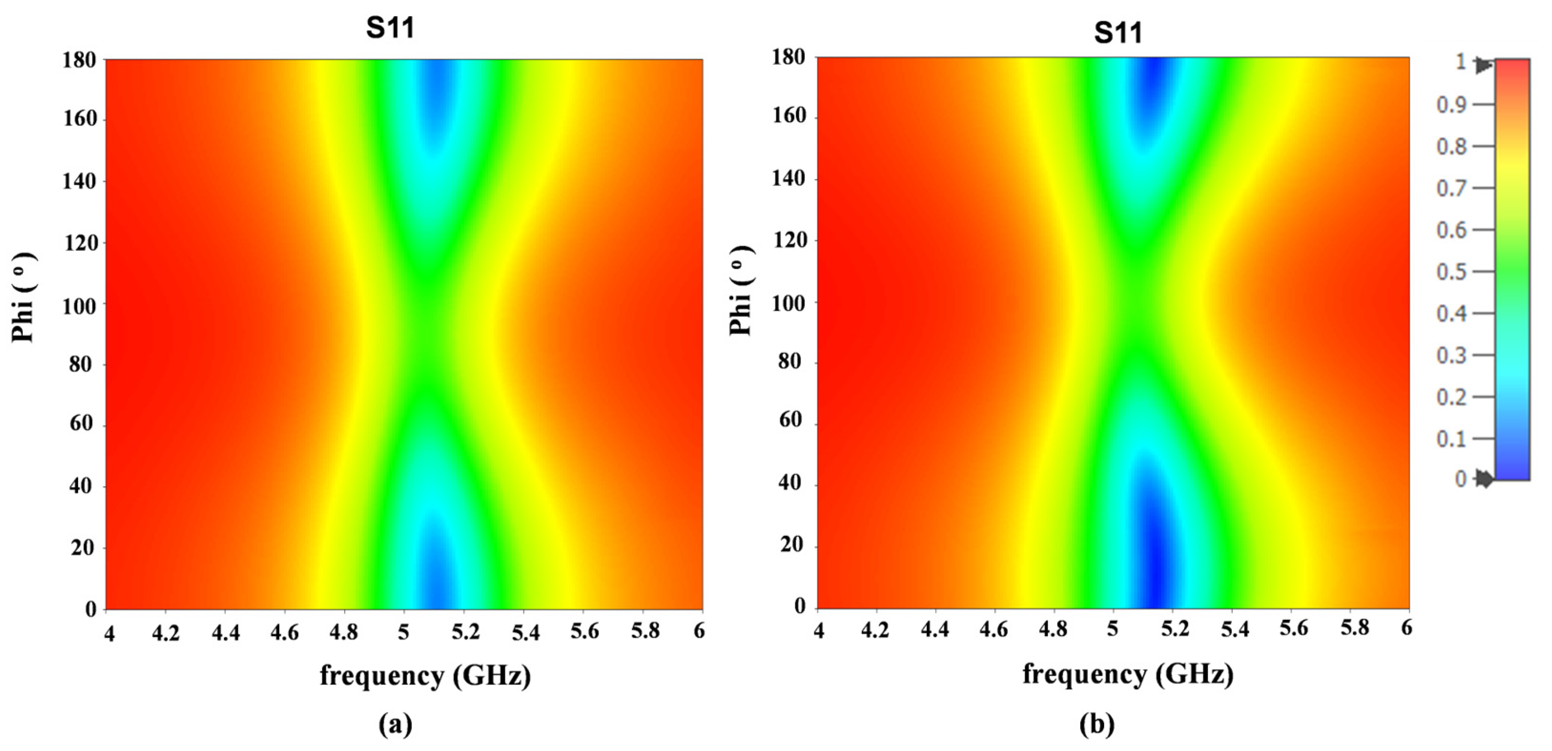
The simulated reflection coefficients for normal incidence, showing both the frequency dependence and the variation with polarization angle (φ) from 0° to 180°, are shown in Figure 2.
It is clear from Figure 2 that the metasurface of the unit cell in Figure 1 (for both models) exhibits a polarization-dependent characteristic when the polarization is varied from 0° to 180°, especially around 5 GHz where the reflection becomes small (absorption becomes large). As shown in Figure 2, the minimum reflection coefficient occurs at 5.122 GHz (absorption > 98%) at φ = 0° and 5.144 GHz (absorption > 99%) at φ = 10°, respectively, based on the two models. These shifts in resonant frequency are mainly caused by changes in the resistor position and structure. The frequency variations in S11 as shown in Figure 2 are mainly due to the resonant behavior of the unit cell, where the interaction between the incident electric field and the lumped resistor varies with polarization angle. Changes in polarization affect the current distribution and impedance matching, leading to variations in the reflection coefficient across frequencies.
The voltage across the lumped resistor is obtained directly from the CST simulation results. This voltage represents the peak (not root mean square, or RMS) amplitude across the resistor. Based on the simulated voltage, the total power harvested across the load R can be calculated using Equation (1), which is as follows:
P l o a d =   V 2 2 R
where V is the voltage amplitude (not the RMS value) of the lumped resistor and P l is the total energy harvested on the lumped resistor R. The lumped resistor was inserted in the unit cell. Choosing the right lumped resistor value can increase the absorption value through impedance matching with free space. The energy absorbed by our structure cannot be completely absorbed by the lumped resistor since some of it is dissipated by dielectric loss in the substrate. In this model, the energy dissipated by dielectric loss is 2.3%. This dielectric loss is frequency-dependent, primarily characterized by the loss tangent (tan δ) which arises from polarization relaxation under time-varying electric fields. Effective metasurface design can minimize energy dissipation during electromagnetic interactions [31].
Figure 3 shows the voltage in each model for normal incidence. Maximum voltage occurs at polarization angles equal to φ p = 0° and 10° for Models A and B, respectively. The polarization angle where the energy absorbed by the lumped resistor is minimum is shown in Figure 3 by the appearance of a minimum voltage that does not depend on frequency. We call this condition the dip phenomenon, which is clearly visible when the voltage across the lumped resistor changes with changing polarization angle, which is a polarization-dependent characteristic. For all models a voltage dip was always found at a specific angle. In the first model, the dip appears at a polarization angle of 90°. In the second model, the dip appears at a polarization angle of 100°. For a geometrical structure the dip phenomenon occurs when the position of the lumped resistor from the center of the patch has an angle of 90° to the direction of the electric field, as shown in Figure 3. It can be analyzed that when the electric field is perpendicular to the line connecting the lumped resistor position and the patch center no effective voltage is developed along that direction on the patch. As a result, no voltage difference is established between the patch and the ground and the lumped resistor does not absorb any current. This misalignment prevents energy from being transferred into the resistive load, leading to negligible power absorption under this condition.
To provide more physical insight into the unit cell of the proposed metasurface, an analysis of the surface current distribution is presented in Figure 4 and Figure 5. In Figure 4, this analysis is conducted at the frequency where power absorption is at its maximum as the polarization angle is varied. The condition of the surface current distribution on the back-side of the unit cell when the electric field is aligned with the position of the lumped resistor from the center of the patch and the voltage on the lumped resistor is at its maximum is shown in Figure 4a,b for Model A at 5.114 GHz ( φ = 0°) and Model B at 5.136 GHz (φ = 10°), respectively. For all models, the current always passes through the circle in the middle (via) with different intensity between the incoming and outgoing sides. The current flow is observed to converge into the via from one side with higher surface current density and to diverge from the other side with lower density, as shown in Figure 4. This imbalance in current density suggests that a portion of the induced surface current is diverted through the via and dissipated by the lumped resistor. This condition occurs when the incident electric field has a component aligned with the direction of the lumped resistor position from the center of the patch, thereby inducing an effective voltage along that direction on the patch. The via, which is shifted from the center of the patch, breaks the geometric symmetry of the unit cell. This asymmetry results in an unbalanced surface current distribution, which enhances the coupling between the incident electric field and the resistive load. As a result a voltage difference between the patch and the ground is developed, enabling current flow through the via which is subsequently absorbed by the lumped resistor. In this configuration the surface patch still supports in-plane current flow, but a portion of the induced surface current is now directed downward through the via into the lumped resistor. This asymmetry allows a net current to enter the resistor. This leads to resistive energy absorption as the induced current flows toward the lumped resistor. Under this condition the metasurface unit cell effectively harvests electromagnetic energy, with clear voltage peaks observable in simulation. Although Figure 4a,b show strong current coupling due to the alignment between the electric field and the resistor position from the center of the patch, the current distribution patterns are slightly different. In Figure 4a, where φp = 0° and the polarization angle φ = 0°, the current is concentrated along the vertical axis (y-direction). In contrast, in Figure 4b, where φp = 10° and φ = 10°, the alignment results in a skew in the current flow concentration. This difference illustrates how variations in the geometric resistor position (φp) influence the orientation of the surface current.
The surface current distribution conditions when a voltage dip appears on the resistor is shown in Figure 5a,b for Model A when the polarization angle is 90° and Model B when the polarization angle is 100°, respectively. For all models the surface current is observed to converge toward the via and subsequently diverge from it, with comparable current density on both the incoming and outgoing paths. This balance indicates that the current flows through the via without being diverted into the lumped resistor, indicating that the lumped resistor does not absorb any current. This occurs when the incident electric field is oriented perpendicular to the direction of the lumped resistor position from the center of the patch, such that it does not induce a potential difference between the patch and the ground. Consequently, no driving voltage is developed across the terminals of the lumped resistor. While the surface patch supports in-plane current flow driven by the incident electric field, these surface currents tend to converge toward the via. However, due to the geometric symmetry of the unit cell an equal amount of current diverges away from the via on the opposite side. This symmetric inflow and outflow form a balanced current pattern, resulting in minimal net current entering the resistor.
As illustrated in Figure 5, the surface currents are distributed symmetrically around the via, and no power is dissipated in the resistor. Under these conditions the structure supports purely reactive surface current flow on the patch, characterized by the storage and exchange of electric and magnetic energy with negligible resistive energy absorption through the via–resistor path. Therefore, in this design the polarization-dependent behavior of the metasurface stems from the use of a single lumped resistor connected through a shifted via, which breaks the symmetry of an otherwise centrally symmetric patch structure, leading to variations in absorption depending on the polarization angle.
The frequency response of the metasurface under varying conditions can be categorized into two distinct effects: shifts caused by structural differences between models and shifts caused by changes in polarization within a single model. The first type of frequency shift arises from differences in the physical structure of the metasurface unit cell, specifically the position of the lumped resistor. In this study, Models A and B utilize point resistors placed along different axes (the y-axis for φp = 0° and the x-axis for φp = 10°, respectively). As shown in Figure 2, even under the same polarization angle these two models exhibit different resonance frequencies. This difference is attributed to variations in the effective resonance conditions caused by the different resistor positions relative to the electric field distribution on the patch. The displacement of the resistor alters the local surface current flow and modifies the electromagnetic coupling, resulting in a shift in the frequency of maximum absorption.
The second type of frequency shift occurs within the same metasurface model when the polarization angle of the incident electric field is varied. For a given structure, rotating the polarization angle changes the alignment between the electric field and the resistor position, thereby altering the strength of the coupling between the incident wave and the resistive load. As a result, small shifts in the absorption frequency are observed as the polarization angle changes. This effect is evident in Models A and B, where variations in φ lead to corresponding shifts in the frequency at which maximum absorption occurs (see Figure 2).
The second case simulation which is also carried out in this paper is that the via and resistor positions are varied at angles ( φ p ) of 30°, 60°, and 90° from the center of the patch, as shown in Figure 6. The simulation results of this case of voltage at the lumped resistor are shown in Figure 7. For each model in the second case, voltage dip appears when the lumped resistor is placed at a 90° angle to the electric field seen from the center of the unit cell. It can be seen that the voltage dips shift with changing lumped resistor positions. This means that there is also a relationship between the position of the lumped resistor and the central point of the patch in capturing RF wave energy.
The relationship between the dip angle and the geometric angle of the structure is shown in Figure 8. Additional simulations were also performed for other angles (15°, 45°, 75°) as well to verify the observed relationship. This condition shows that there will always be a dip wherever the resistor is placed, which means polarization-independence will not be possible with this design. There are two points emphasized by these results: (1) the dip angle does not depend on frequency but is determined by the geometry of the structure itself; (2) there is a clear relationship between the position of the resistor relative to the center of the patch and the resulting dip angle. To further validate this observation we also simulated a circular patch structure using one via and a resistor, and we confirmed a similar relationship between the resistor position from the patch center and the dip angle.

3.2. Measurement Results

To validate the polarization characteristics of the square patch metasurface energy-harvesting experimentally, four 10 × 10 arrays were fabricated, with via positions from the center of the patch ( φ p ) at angles of 0°, 30°, 45°, and 60°, as shown in Figure 9a,b. The 10 × 10 array configuration was selected to provide an adequate electromagnetic response for experimental validation, minimizing edge effects and enhancing the measurement accuracy of the metasurface’s polarization characteristics.
The metasurface was fabricated using an FR-4 substrate with a thickness of 1 mm, and other parameters were set to be the same as those listed in Table 1. The total size of each 10 × 10 array is 15 cm × 15 cm. The front of the unit cell and the back-side of the ground plane were coated with a green resist to prevent oxidation and avoid short circuits during component soldering. A dedicated soldering pad pattern was provided on each unit cell on the ground plane for mounting a lumped resistor or a connector, as shown in Figure 9b. The metasurface was illuminated by a horn antenna connected to a vector network analyzer (VNA) positioned at a distance of 110 cm (R = 110 cm), providing incident power uniformly across all unit cells. The distance R was determined based on the horn antenna’s aperture to ensure far-field conditions. All measurements were conducted inside an anechoic chamber to eliminate reflections and external electromagnetic interference. In the experimental setup shown in Figure 9c, a Rohde & Schwarz ZVB VNA and an A-INFO LB-10125-SF broadband horn antenna were used to measure the transmission coefficient (S21) of the designed metasurface. The VNA was calibrated using the UOSM (Unknown Through–Open–Short–Match) method with a Rohde & Schwarz ZN-Z51 calibration kit, including the connected cables, prior to conducting the measurements. The S21 parameter, representing the harvested signal through the lumped resistor, was then compared with the simulation results. The central unit cell was chosen for measurement due to its minimal edge effects and closest to the conditions of an infinite array. The measurement connection was established using a U.FL connector, which was soldered onto the metasurface and modeled in the simulation as a lumped resistor oriented in a specific direction. To emulate the electromagnetic coupling environment observed in the simulations, all other output ports from the unit cells in the array were terminated with 50 Ω loads by soldering lumped resistors onto the designated pads (see Figure 9b). To vary the polarization angle during the experiment the metasurface was rotated while the transmitting horn remained stationary. The center of the metasurface was precisely aligned with the center of the horn’s aperture.
To make a fair comparison between simulation and measurement, the measured S21 parameter from the VNA is interpreted as an indicator of the voltage across the 50 ohm resistor. In the experiment, the metasurface was illuminated by a plane wave, and the central unit cell was connected to port 2 of the VNA through a matched coaxial connector. The S21 value thus reflects the amount of power that is harvested and delivered through the lumped resistor.
Although S21 is measured as a transmission coefficient, it can be considered proportional to the voltage across the resistor under the assumption of proper impedance matching. While absolute values may differ slightly due to losses or imperfections, the measured S21 remains a reliable proxy for comparing the polarization response of the system. To compare the simulation and measurement results, both datasets were normalized so that their maximum values correspond to the same reference point. This normalization allows a direct visual comparison of the voltage trends as a function of the polarization angle.
As shown in Figure 10, the measurement results confirm the simulation results that the square patch metasurface energy harvesting using one via and one resistor has polarization-dependent characteristics. This can be observed from the change in voltage value against the polarization angle, which is consistent with the measurement and simulation results. Therefore, the key outcome is the agreement achieved between the measurement and simulation results. Both the simulation and measurement results exhibit a voltage dip at the same polarization angle for each design; however, the dip observed in the measurement is not as deep as that in the simulation. The difference in polarization angular characteristics, particularly in terms of voltage dip, can be attributed to practical factors present in the measurement setup. These include edge effects from the finite metasurface array, parasitic elements from coaxial cable connections, minor misalignments during rotation, and the influence of measurement noise. The simulation assumes an ideal infinite array with perfect symmetry and noiseless conditions. A small shift in the frequency of the maximum voltage was observed between the simulation and measurement results for each metasurface model, ranging from 174 MHz to 234 MHz. Specifically, for the designs with via positions φp = 0°, 30°, 45°, and 60°, the simulated maximum voltage frequency was consistently 5.114 GHz, while the corresponding measured frequencies were 4.88 GHz, 4.91 GHz, 4.90 GHz, and 4.94 GHz, respectively. The shift in maximum voltage frequency may arise from fabrication-related imperfections, such as slight deviations in via placement, soldering inaccuracies in the lumped resistor connections, and the connector. Furthermore, material properties such as the dielectric constant and loss tangent of the FR-4 substrate may be different from the ideal values used in simulations, contributing to the observed frequency offset.

4. The Asymmetric Case

The asymmetric case used a square patch for the first case (Model A). Specifically, one of the corners was trimmed by connecting two points: one located 4 mm along the horizontal (x-axis) direction from the top-left corner, and another located 4 mm downward (along the y-axis) from the same corner. A straight diagonal line was drawn between these two points to create the chamfered edge, resulting in an asymmetrical polygonal shape, as illustrated in Figure 11a. Aside from this geometric modification, all other structural parameters remain identical to those of the first case (Model A). This model is also evaluated through simulations and experiments under linearly polarized wave incidence. The purpose of evaluating the asymmetric structure is to investigate whether introducing geometric asymmetry can mitigate the severe voltage dips observed in symmetric designs, rather than to achieve full polarization independence. As shown in Figure 11a, the asymmetric model demonstrates a smoother voltage profile with reduced sharp voltage dips across the frequency range, even when the polarization angle is varied. This indicates that the asymmetrical structure helps modify the surface current distribution in a way that is less sensitive to changes in polarization, reducing the occurrence of sharp voltage dips. Although the asymmetric structure does not eliminate polarization dependence entirely it significantly mitigates voltage dips, leading to more stable energy harvesting performance. In addition, the dip angle varies with frequency because the surface current changes in a complex manner, depending on the relationship between the electric field direction, the position of the via (resistor), and the shape of the cut.
Figure 11b shows a comparison between the simulated voltage responses of the asymmetric patch model (blue line) and the symmetric patch model (Model A, orange line) as a function of polarization angle from 0° to 180°. The results are shown for fixed operating frequencies corresponding to the maximum voltage observed in each design based on earlier simulations: 5.114 GHz for the symmetric case (see Figure 3a) and 4.998 GHz for the asymmetric case (see Figure 11a). Figure 11b clearly shows that the symmetric patch (Model A) exhibits a sharp voltage dip at 90° polarization, indicating high sensitivity to polarization angle. In contrast, the asymmetric patch maintains a more stable voltage response across the entire polarization range, demonstrating less sensitivity. However, this stability comes with a lower maximum voltage as the peak voltage for the asymmetric case reaches 12.7 dBV, while the symmetric design reaches a higher maximum of 14.7 dBV. This reduction in voltage is due to the asymmetric geometry, which interacts more favorably with circularly polarized components and less effectively with linearly polarized waves. This observation clearly illustrates a performance trade-off. The asymmetric structure sacrifices approximately 2 dB in peak voltage compared to the symmetric case, which corresponds to roughly a 37% reduction in power efficiency. However, it offers improved robustness across varying polarization angles. Such robustness is particularly valuable for practical RF energy harvesting applications where the incident polarization may vary unpredictably or randomly over time.
To validate the simulation results, measurements were also conducted on the asymmetric model. As shown in Figure 11c, the measurement results for the asymmetric shape confirm that this shape can reduce sensitivity to changes in the polarization angle, which is clearly visible through a less sharp voltage drop compared to the symmetric shape shown in Figure 10. These measurements align well with the simulation results. The voltage drop observed in the measurements is slightly deeper than in the simulations, which can be attributed to the fact that the asymmetric model was physically created by cutting the fabricated symmetric structure. Such manual modifications may introduce non-ideal edge geometry, surface roughness, or slight discontinuities, locally altering the current distribution and increasing polarization sensitivity. A shift in the maximum voltage frequency is also observed between the simulation and measurement; the simulated maximum occurs at 4.998 GHz, while the measured maximum is at 4.75 GHz. This shift may result from fabrication imperfections, such as minor deviations in via placement, inaccuracies during manual cutting, soldering of the connected resistors, and connector issues. Material properties, like the dielectric constant and loss tangent of the FR-4 substrate, may also differ from the ideal values used in the simulation, contributing to the shift in the maximum voltage frequency.

5. Conclusions

This paper presents a systematic investigation into the polarization characteristics of a symmetrical, square patch metasurface unit cell designed for RF energy harvesting, using a single via and a single lumped resistor. Both simulation and experimental results exhibit polarization-dependent characteristics and confirm the existence of a voltage dip at specific polarization angles, which occurs when the direction of the electric field is perpendicular to the position of the resistor relative to the center of the patch. This behavior reveals a fundamental sensitivity to polarization in such structures.
The key novel contribution of this work is the establishment and experimental validation of a linear relationship between the geometric position angle of the resistor and the resulting polarization dip angle. This relationship is consistently demonstrated across both simulation and measurement and is independent of frequency. Unlike previous studies that only reported polarization characteristics at a limited number of polarization angles, this paper presents a predictive design rule that enables engineers to determine the dip angle directly from the resistor’s geometric placement. This insight sets the present work apart and provides a quantitative foundation for future metasurface design strategies involving polarization-dependent behavior.
Additionally, this study explored, through both simulation and measurement, an asymmetric patch design as a potential approach to mitigate sharp voltage dips and improve stability under varying polarization conditions. While asymmetry reduces dip sharpness it also leads to a decrease in absorption efficiency under linearly polarized waves. Therefore, designers must balance robustness to polarization variations with maximum energy harvesting performance depending on the intended application. In conclusion, the findings of this study provide a new framework for designing metasurface energy harvesters based on predictable and tunable polarization behavior. Further analysis of polarization-dependent behavior based on detailed analysis through equivalent circuit models or field distribution theory will enhance the applicability of this work. Future research may also include further exploration of both various symmetric and asymmetric geometries, investigation over wider frequency bands, and consideration of fabrication-related effects that may influence dip characteristics and measurement accuracy.

Author Contributions

Conceptualization, E.M.P. and S.Y.; methodology, E.M.P.; validation, E.M.P. and S.Y.; formal analysis, E.M.P.; investigation, E.M.P. and S.Y.; resources, S.Y.; writing—original draft preparation, E.M.P.; writing—review and editing, S.Y., T.I. and M.O.; supervision, S.Y. All authors have read and agreed to the published version of the manuscript.

Funding

This research received no external funding.

Institutional Review Board Statement

Not applicable.

Informed Consent Statement

Not applicable.

Data Availability Statement

The original contributions presented in the study are included in the article, further inquiries can be directed to the corresponding authors.

Acknowledgments

The first author would like to express gratitude to the Ministry of Education, Culture, Sports, Science, and Technology (MEXT) Japan and the Japan International Cooperation Agency (JICA) for providing the scholarship during the study at Kanazawa University, Japan.

Conflicts of Interest

The authors declare no conflicts of interest.

References

  1. Valenta, C.R.; Durgin, G.D. Harvesting wireless power: Survey of energy-harvester conversion efficiency in far-field, wireless power transfer systems. IEEE Microw. Mag. 2014, 15, 108–120. [Google Scholar] [CrossRef]
  2. Kim, S.; Vyas, R.; Bito, J.; Niotaki, K.; Collado, A.; Georgiadis, A.; Tentzeris, M.M. Ambient RF energy-harvesting technologies for self-sustainable standalone wireless sensor platforms. Proc. IEEE 2014, 102, 1649–1666. [Google Scholar] [CrossRef]
  3. Nie, M.J.; Yang, X.X.; Tan, G.N.; Han, B. A compact 2.45-GHz broadband rectenna using grounded coplanar waveguide. IEEE Antennas Wirel. Propag. Lett. 2015, 14, 986–989. [Google Scholar] [CrossRef]
  4. Song, C.; Huang, Y.; Carter, P.; Zhou, J.; Yuan, S.; Xu, Q.; Kod, M. A Novel Six-Band Dual CP Rectenna Using Improved Impedance Matching Technique for Ambient RF Energy Harvesting. IEEE Trans. Antennas Propag. 2016, 64, 3160–3171. [Google Scholar] [CrossRef]
  5. Cai, W.; Chettiar, U.K.; Kildishev, A.V.; Shalaev, V.M. Optical cloaking with metamaterials. Nat. Photonics 2007, 1, 224–227. [Google Scholar] [CrossRef]
  6. Chen, H.-Y.; Wang, J.-F.; Ma, H.; Qu, S.-B.; Zhang, J.-Q.; Xu, Z.; Zhang, A.-X. Broadband perfect polarization conversion metasurfaces. Chin. Phys. B 2015, 24, 014201. [Google Scholar] [CrossRef]
  7. Zhu, J.; Eleftheriades, G.V. Dual-band metamaterial-inspired small monopole antenna for WiFi applications. Electron. Lett. 2009, 45, 1104–1106. [Google Scholar] [CrossRef]
  8. Erentok, A.; Ziolkowski, R.W. Metamaterial-inspired efficient electrically small antennas. IEEE Trans. Antennas Propag. 2008, 56, 691–707. [Google Scholar] [CrossRef]
  9. Fang, N.; Zhang, X. Imaging properties of a metamaterial superlens. Appl. Phys. Lett. 2003, 82, 161–163. [Google Scholar] [CrossRef]
  10. Aydin, K.; Bulu, I.; Ozbay, E. Subwavelength resolution with a negative-index metamaterial superlens. Appl. Phys. Lett. 2007, 90, 254102. [Google Scholar] [CrossRef]
  11. Abdulkarim, Y.I.; Deng, L.; Altıntaş, O.; Ünal, E.; Karaaslan, M. Metamaterial absorber sensor design by incorporating swastika shaped resonator to determination of the liquid chemicals depending on electrical characteristics. Phys. E Low-Dimens. Syst. Nanostructures 2019, 114, 113593. [Google Scholar] [CrossRef]
  12. Tabassum, S.; Nayemuzzaman, S.K.; Kala, M.; Mishra, A.K.; Mishra, S.K. Metasurfaces for Sensing Applications: Gas, Bio and Chemical. Sensors 2022, 22, 6896. [Google Scholar] [CrossRef] [PubMed]
  13. Zheng, N.; Aghadjani, M.; Song, K.; Mazumder, P. Metamaterial sensor platforms for Terahertz DNA sensing. In Proceedings of the 13th IEEE International Conference on Nanotechnology (IEEE-NANO 2013), Beijing, China, 5–8 August 2013; pp. 315–320. [Google Scholar] [CrossRef]
  14. Landy, N.I.; Sajuyigbe, S.; Mock, J.J.; Smith, D.R.; Padilla, W.J. Perfect metamaterial absorber. Phys. Rev. Lett. 2008, 100, 207402. [Google Scholar] [CrossRef] [PubMed]
  15. Dincer, F.; Karaaslan, M.; Sabah, C. Design and analysis of perfect metamaterial absorber in GHz and THz frequencies. J. Electromagn. Waves Appl. 2015, 29, 2492–2500. [Google Scholar] [CrossRef]
  16. Wen, Z.; Wang, W.; Khelif, A.; Djafari-Rouhani, B.; Jin, Y. A perspective on elastic metastructures for energy harvesting. Appl. Phys. Lett. 2022, 120, 020501. [Google Scholar] [CrossRef]
  17. Ramahi, O.M.; Almoneef, T.S.; Alshareef, M.; Boybay, M.S. Metamaterial particles for electromagnetic energy harvesting. Appl. Phys. Lett. 2012, 101, 173903. [Google Scholar] [CrossRef]
  18. Shang, S.; Yang, S.; Liu, J.; Shan, M.; Cao, H. Metamaterial electromagnetic energy harvester with high selective harvesting for left- and right-handed circularly polarized waves. J. Appl. Phys. 2016, 120, 045106. [Google Scholar] [CrossRef]
  19. Ohmae, A.; Yagitani, S. Direction-of-Arrival Estimation With Planar Luneburg Lens and Waveguide Metasurface Absorber. IEEE Access 2023, 11, 21968–21976. [Google Scholar] [CrossRef]
  20. Alkurt, F.O.; Altintas, O.; Atci, A.; Bakir, M.; Unal, E.; Akgol, O.; Delihacioglu, K.; Karaaslan, M.; Sabah, C. Antenna-based microwave absorber for imaging in the frequencies of 1.8, 2.45, and 5.8 GHz. Opt. Eng. 2018, 57, 113102. [Google Scholar] [CrossRef]
  21. Yagitani, S.; Katsuda, K.; Nojima, M.; Yoshimura, Y.; Sugiura, H. Imaging radio-frequency power distributions by an EBG absorber. IEICE Trans. Commun. 2011, E94-B, 2306–2315. [Google Scholar] [CrossRef]
  22. Ullah, N.; Islam, M.S.; Haque, A.; Yong, W.H.; Soliman, M.S.; Albadran, S.; Islam, M.T. A compact complementary split ring resonator (CSRR) based perfect metamaterial absorber for energy harvesting applications. Eng. Sci. Technol. Int. J. 2023, 45, 101473. [Google Scholar] [CrossRef]
  23. Wang, N.; Dong, X.; Zhou, W.; He, C.; Jiang, W.; Hu, S. Low-frequency metamaterial absorber with small-size unit cell based on corrugated surface. AIP Adv. 2016, 6, 025205. [Google Scholar] [CrossRef]
  24. Cheng, Y.; Zou, H.; Yang, J.; Mao, X.; Gong, R. Dual and broadband terahertz metamaterial absorber based on a compact resonator structure. Opt. Mater. Express 2018, 8, 3104. [Google Scholar] [CrossRef]
  25. Li, Y.; Assouar, B.M. Acoustic metasurface-based perfect absorber with deep subwavelength thickness. Appl. Phys. Lett. 2016, 108, 063502. [Google Scholar] [CrossRef]
  26. Paradiso, J.A.; Starner, T. Energy scavenging for mobile and wireless electronics. IEEE Pervasive Comput. 2005, 4, 18–27. [Google Scholar] [CrossRef]
  27. Ghaneizadeh, A.; Gavriilidis, P.; Joodaki, M.; Alexandropoulos, G.C. Metasurface Energy Harvesters: State-of-the-Art Designs and Their Potential for Energy Sustainable Reconfigurable Intelligent Surfaces. IEEE Access 2024, 12, 160464–160494. [Google Scholar] [CrossRef]
  28. Yu, F.; Yang, X.; Zhong, H.; Chu, C.; Gao, S. Polarization-insensitive wide-angle-reception metasurface with simplified structure for harvesting electromagnetic energy. Appl. Phys. Lett. 2018, 113, 123903. [Google Scholar] [CrossRef]
  29. Yu, F.; He, G.Q.; Yang, X.X.; Du, J.; Gao, S. Polarization-insensitive metasurface for harvesting electromagnetic energy with high efficiency and frequency stability over wide range of incidence angles. Appl. Sci. 2020, 10, 8047. [Google Scholar] [CrossRef]
  30. Zhang, X.; Liu, H.; Li, L. Electromagnetic Power Harvester Using Wide-Angle and Polarization-Insensitive Metasurfaces. Appl. Sci. 2018, 8, 497. [Google Scholar] [CrossRef]
  31. Li, L.; Zhang, X.; Song, C.; Huang, Y. Progress, challenges, and perspective on metasurfaces for ambient radio frequency energy harvesting. Appl. Phys. Lett. 2020, 116, 060501. [Google Scholar] [CrossRef]
Figure 1. The proposed first case unit cell of metasurface. (a) Perspective view. (b) Front view. (c) Back view for Models A and B. φ defines the polarization angle and φ p defines the geometric angle position of the resistor from the center of the patch.
Applsci 15 08561 g001
Figure 2. Reflection coefficients for the unit cell in Figure 1 for normal incidence with different polarization angles. (a) Model A and (b) Model B.
Applsci 15 08561 g002
Figure 3. The voltage on the unit cell of the first case in Figure 1 for normal incidence with different polarization angles: (a) Model A and (b) Model B.
Applsci 15 08561 g003
Figure 4. Surface current distribution around the via, viewed from the back-side of the patch of the unit cell for the metasurface in Figure 1, when the electric field is aligned with the position of the lumped resistor from the center of the patch and the voltage across the resistor is at its maximum: (a) first model at 5.114 GHz, and (b) second model at 5.136 GHz. The left panel: front view of the unit cell with the area inside the box as the focus of the surface current distribution display. The middle panels: surface current distribution contour on the back-side of the patch. The right panels: surface current distribution arrows on the back-side of the patch.
Applsci 15 08561 g004
Figure 5. Surface current distribution around the via on the back-side of the patch for the metasurface in Figure 1, when the electric field is perpendicular with the position of the lumped resistor from the center of the patch and the voltage on the resistor is minimum (dip appears): (a) first model at 5.114 GHz, (b) second model at 5.136 GHz. The left panel: front view of unit cell with the area inside the box as the focus of the surface current distribution display. The middle panels: surface current distribution contour on the back-side of the patch. The right panels: surface current distribution arrows on the back-side of the patch.
Applsci 15 08561 g005
Figure 6. The proposed second case unit cell of metasurface with variations of φ p . (a) Front view, (b) back view.
Applsci 15 08561 g006
Figure 7. The voltage on the unit cell of the second case with different polarization angles from 0° to 180°. (a) φ p = 30°, (b) φ p = 60°, (c) φ p = 90°.
Applsci 15 08561 g007
Figure 8. The relationship between dip angle of voltage and geometry angle position of resistor from center of the patch. A blue dashed line represents a linear relation between dip angle of voltage and geometry angle position of resistor from center of the patch.
Applsci 15 08561 g008
Figure 9. Fabricated 10 × 10 array of the metasurface unit cells: (a) the top and (b) the bottom. (c) The measurement setup used in the experiment.
Applsci 15 08561 g009
Figure 10. Measurement and simulation results from (a) φ p = 0°, (b) φ p = 30°, (c) φ p = 45°, (d) φ p = 60°.
Applsci 15 08561 g010
Figure 11. (a) The asymmetric model of the unit cell and the simulated voltage results. The black dashed line represents the frequency-dependent position of the voltage dips. (b) Comparison of simulation results of the voltage on the asymmetric model (blue line) and symmetric model of the first case Model A (orange line). (c) Comparison of measurement and simulation results for the voltage on the asymmetric model at the maximum voltage frequencies of 4.75 GHz and 4.998 GHz, respectively. Simulation results are the blue line and measurement results are the orange dots.
Applsci 15 08561 g011
Table 1. Descriptions of the structure parameters.
ParametersDimension (mm)
s15
l13
m3.25
d1.2
Disclaimer/Publisher’s Note: The statements, opinions and data contained in all publications are solely those of the individual author(s) and contributor(s) and not of MDPI and/or the editor(s). MDPI and/or the editor(s) disclaim responsibility for any injury to people or property resulting from any ideas, methods, instructions or products referred to in the content.

