
A 0.3 V Current Differencing Buffered Amplifier and Its Application in Current-Mode Third-Order Low-Pass Filters


Abstract
1. Introduction
2. Circuit Description
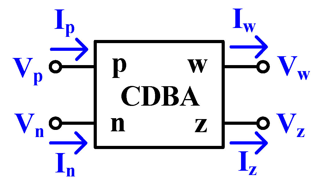
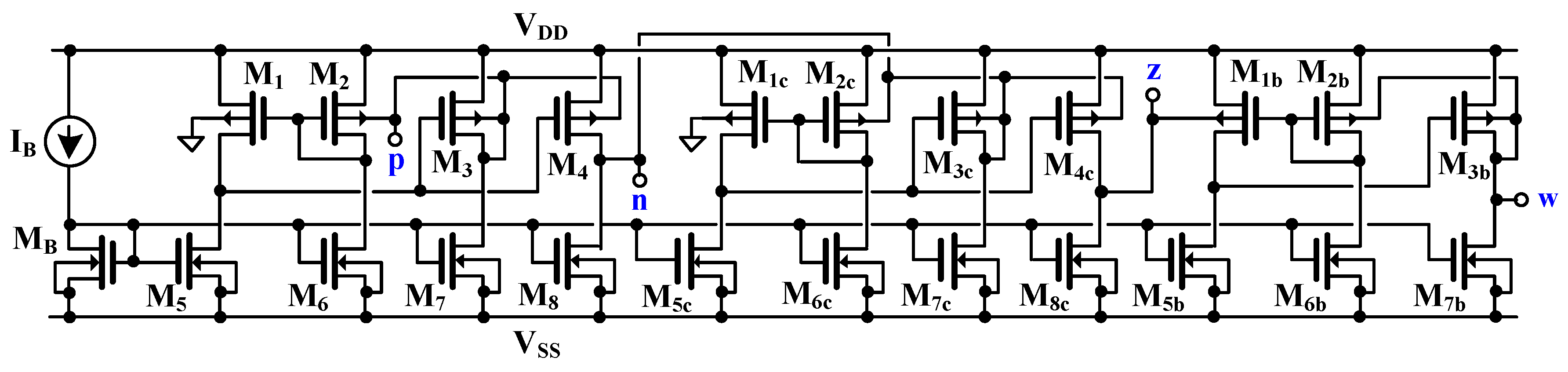
2.1. Proposed 0.3 V CDBA
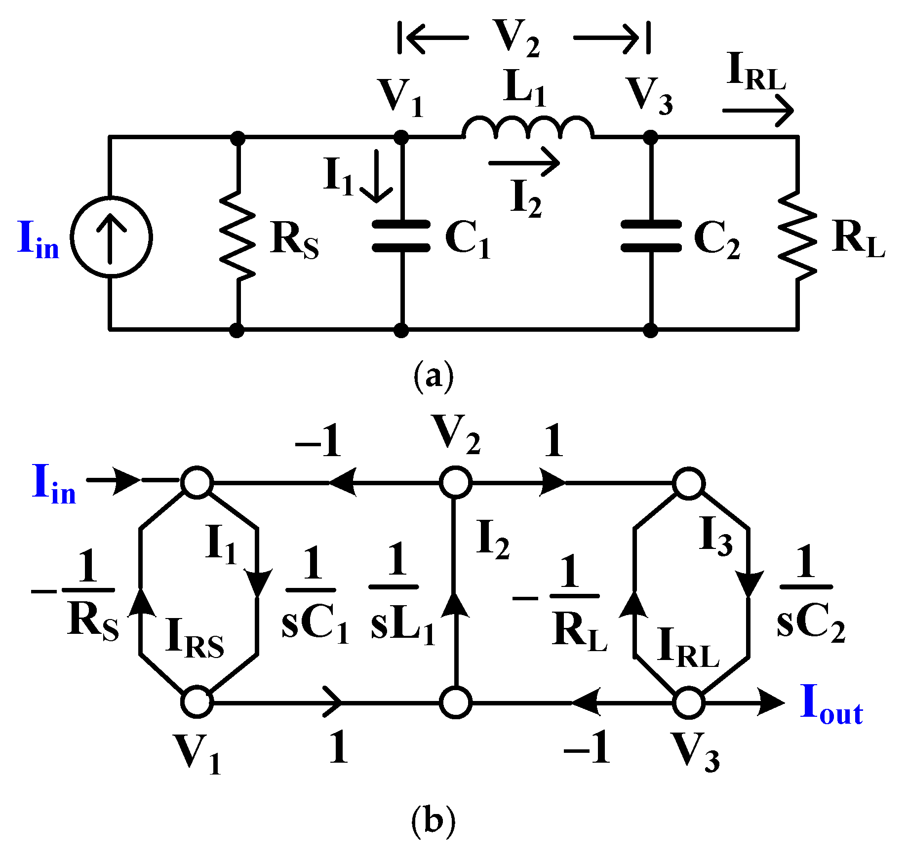
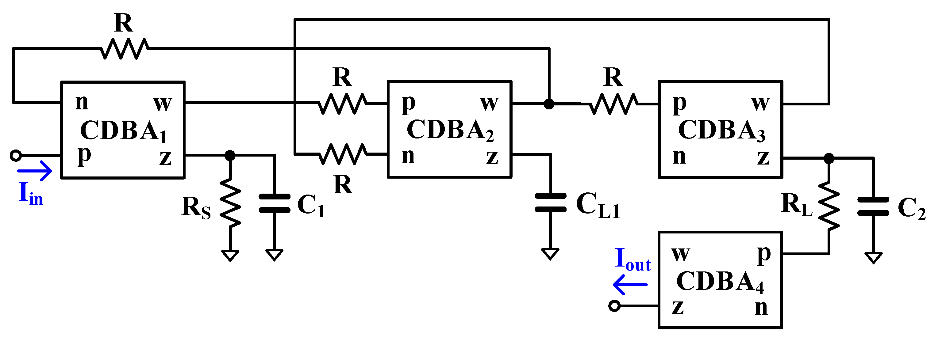
2.2. Proposed Filter
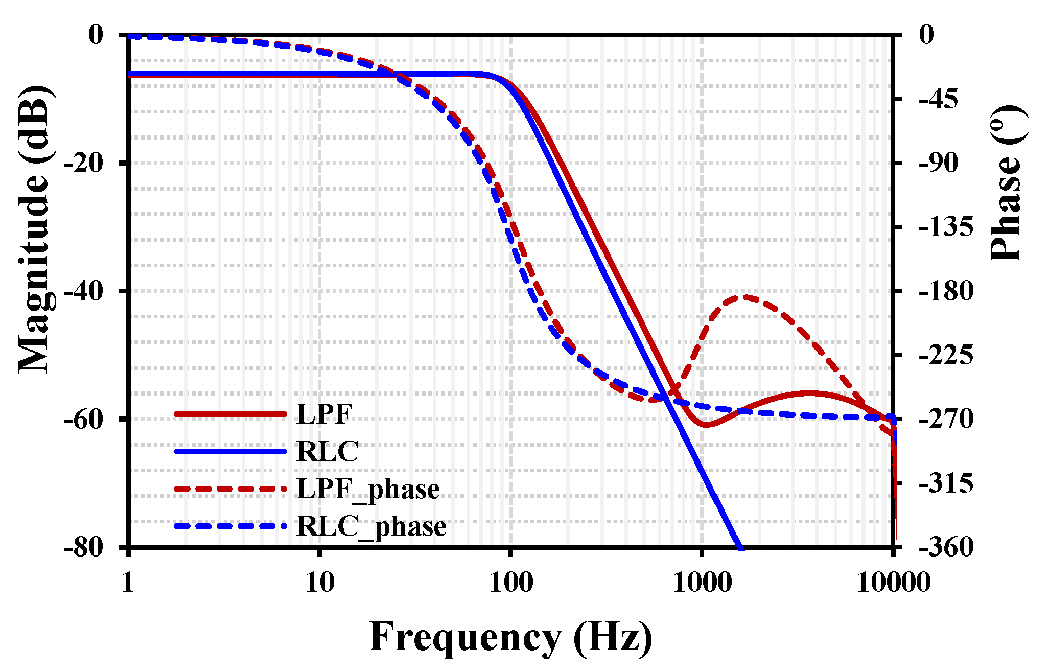
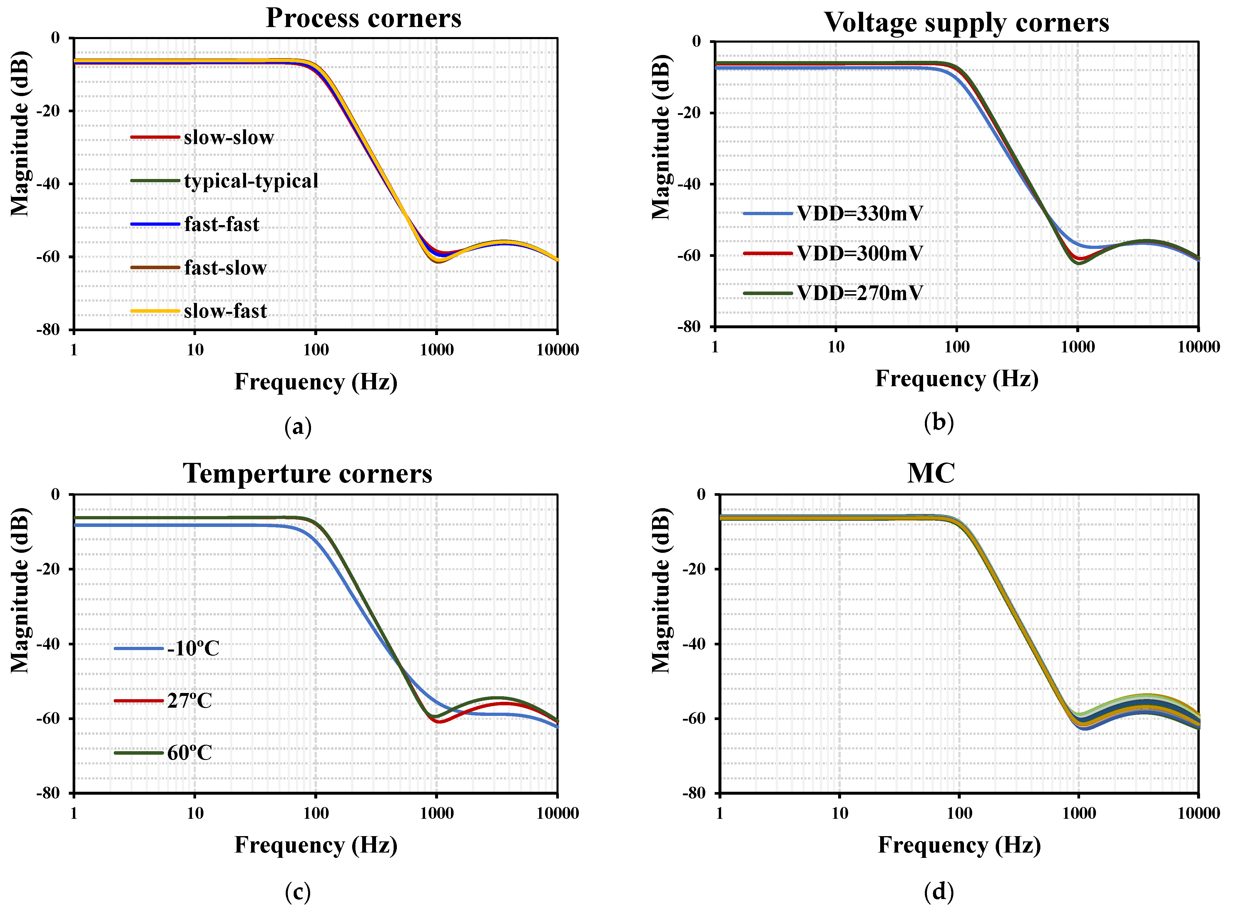
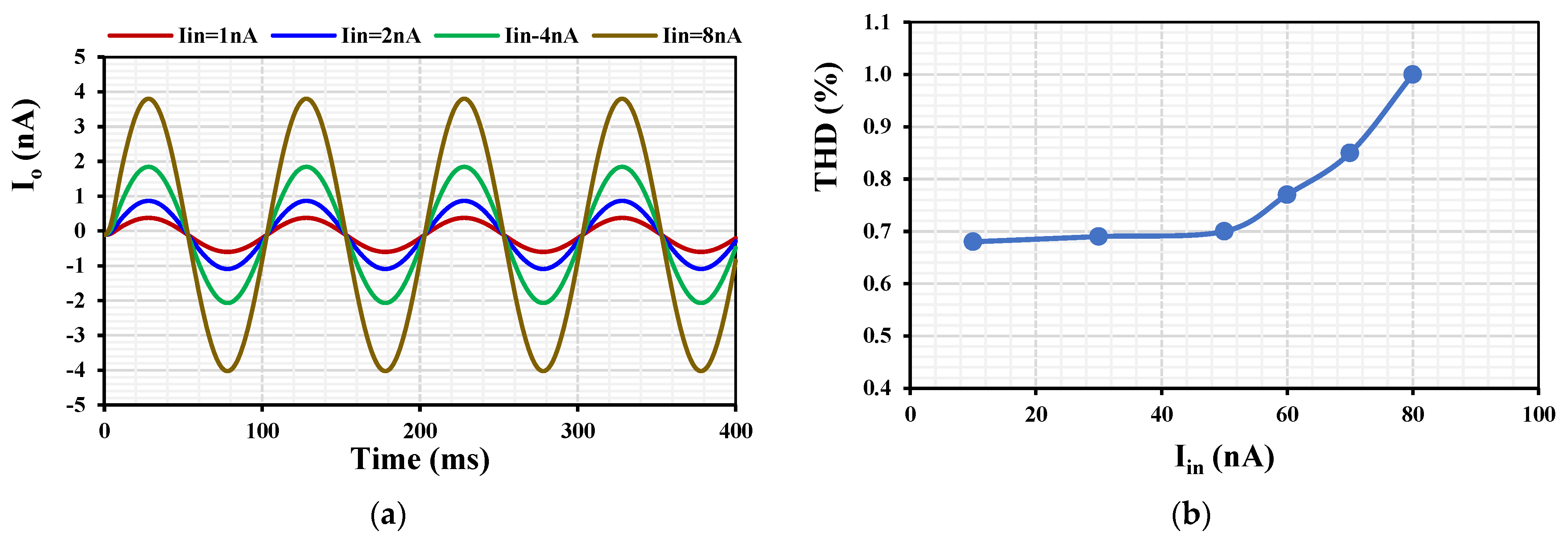
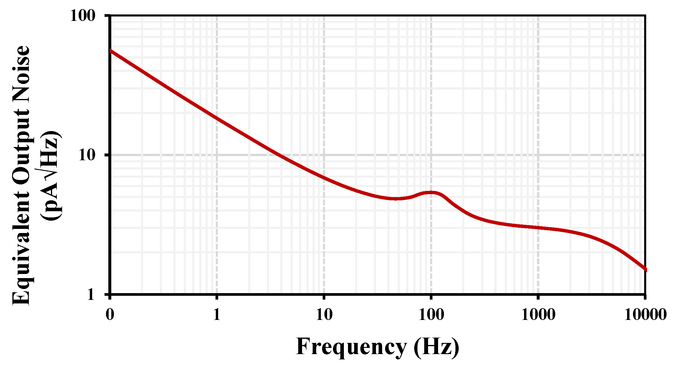
3. Results

| Parameters | Value |
|---|---|
| Supply voltage | 0.3 V |
| Bias current | 10 nA |
| Technology | 0.18 μm |
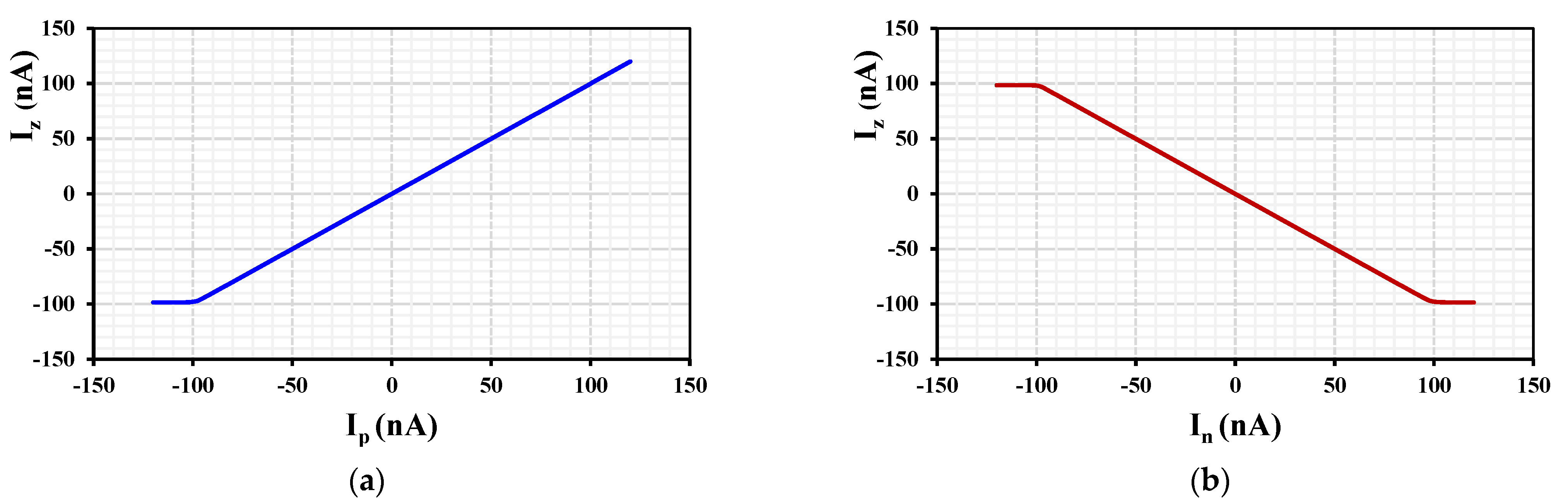
| DC current swings: | ±100 nA |
| Current gains: | 0.997, 0.998 |
| Current offset = 0) | 1.35 nA |
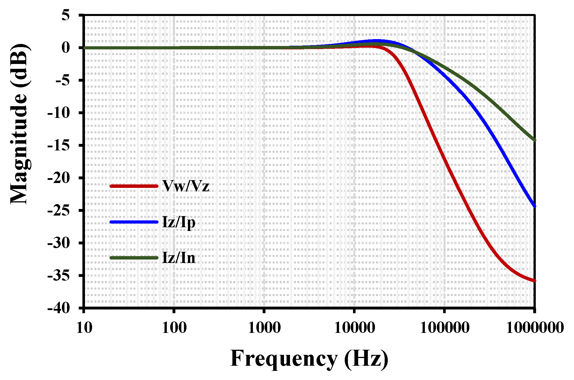
| –3 dB bandwidth: | [79.4, 100] kHz |
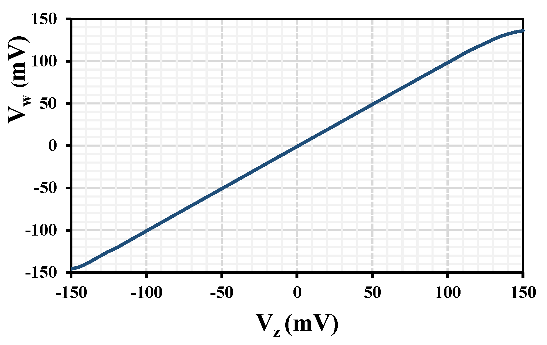
| DC voltage swings: | ±120 mV |
| Voltage gain: | 0.996 |
| Voltage offset = 0) | 2.4 mV |
| –3 dB bandwidth:= 5pF) | 35 kHz |
| 17 kΩ | |
| 24.5 MΩ | |
| Power dissipation | 170 nW |
| Factor | Unit | Proposed | [12] 2006 | [29] 2010 | [31] 2014 | [49] 2024 |
|---|---|---|---|---|---|---|
| Technology | µm | 0.18 | 0.5 | 0.18 | 0.18 | 0.045 |
| Voltage supply | V | 0.3 | ±1.25 | ±0.6 | ±1 | ±0.6 |
| Power consumption | nW | 170 | 0.93 × 10⁶ | 565.25 × 10³ | 1.58 × 10⁶ | 271.9 × 10³ |
| Current gains: | - | 0.997, 0.998 | 0.991, 0.996 | 0.981, 0.981 | 1.015, 1.015 | 0.75, 0.75 |
| Voltage gain: | - | 0.996 | 0.989 | 0.978 | 0.995 | 0.941 |
| DC current swing: | nA | ±100 | ~±30 × 103 | ~±50 × 103 | ±50 × 103 | - |
| DC offset | nA | 1.35 * | 0.49 × 10⁶ | 0.05 × 10⁶ | - | 4.6 |
| DC voltage swing: | mV | ±120 | ~±75 | ~±75 | ±215 | ~±180 |
| −3 dB bandwidth: | kHz | 79.4, 100 | 580 × 103, 643 × 103 | 25 × 103, 25 × 103 | 238.84 × 10³, 174.65 × 10³ | 20 × 103, 20 × 103 |
| −3 dB bandwidth: | kHz | 5pF) | 570 × 103 | 474 × 103 | 243.43 × 10³ | 657.8 × 10³ |
| kΩ | 17 | 14 | 56.4 | 263.77 | - | |
| kΩ | 17 | 14 | 56.4 | 161.15 | - | |
| kΩ | 17 | 14 | 270 | 214.67 | - | |
| MΩ | 21.5 | 0.29 | 0.157 | 0.242 | - | |
| Achieved result | - | Sim. | Sim. | Sim. | Post-Layout Sim. | Sim. |

4. Conclusions
Author Contributions
Funding
Institutional Review Board Statement
Informed Consent Statement
Data Availability Statement
Conflicts of Interest
References
- Acar, C.; Ozoguz, S. A new versatile building block: Current differencing buffered amplifier suitable for analog signal-processing filters. Microelectron. J. 1999, 30, 157–160. [Google Scholar] [CrossRef]
- Ozoguz, S.; Toker, A.; Acar, C. Current-mode continuous-time fully-integrated universal filter using CDBAs. Electron. Lett. 1999, 35, 97–98. [Google Scholar] [CrossRef]
- Sedef, H.; Acar, C. On the Realisation of Voltage-Mode Filters Using CDBA. Frequenz 2000, 54, 198–202. [Google Scholar] [CrossRef]
- Salama, K.N.; Soliman, A.M. Voltage mode Kerwin-Huelsman-Newcomb Circuit Using CDBAs. Frequenz 2000, 54, 90–93. [Google Scholar] [CrossRef]
- Tangsrirat, W.; Surakampontorn, W. Realization of multiple-output biquadratic filters using current differencing buffered amplifiers. Int. J. Electron. 2005, 92, 313–325. [Google Scholar] [CrossRef]
- Maheshwari, S.; Khan, I.A. Novel voltage-mode universal filter using only two CDBAs. J. Circuits Syst. Comput. 2005, 14, 159–164. [Google Scholar] [CrossRef]
- Tangsrirat, W.; Prasertsom, D.; Surakampontorn, W. Low-voltage digitally controlled current differencing buffered amplifier and its application. AEU Int. J. Electron. Commun. 2009, 63, 249–258. [Google Scholar] [CrossRef]
- Hwang, Y.-S.; Huang, Z.-H.; Chen, J.-J.; Lee, W.-T. High-Order Current-Mode Filters Based on Current Differencing Buffered Amplifiers. In Proceedings of the 2007 International Conference on Communications, Circuits and Systems, Kokura, Japan, 11–13 July 2007; pp. 999–1002. [Google Scholar] [CrossRef]
- Acar, C.; Ozoguz, S. Nth-order current transfer function synthesis using current differencing buffered amplifier: Signal-flow graph approach. Microelectron. J. 2000, 31, 49–53. [Google Scholar] [CrossRef]
- Tangsrirat, W.; Surakampontorn, W.; Fujii, N. Realization of Leapfrog Filters Using Current Differential Buffered Amplifiers. EICE Transactions on Fundamentals of Electronics. Commun. Comput. Sci. 2003, E86-A, 318–326. [Google Scholar]
- Biolek, D.; Olsak, M.; Biolekova, V. Optimization of elliptic leap-frog CDBA-based filters. Comput. Methods Circuits Syst. Appl. 2003, 1, 221–225. [Google Scholar]
- Tangsrirat, W.; Klahan, K.; Dumawipata, T.; Surakampontorn, W. Low-voltage NMOS-based current differencing buffered amplifier and its application to current-mode ladder filter design. Int. J. Electron 2006, 93, 777–791. [Google Scholar] [CrossRef]
- Ghosh, M.; Mondal, P.; Kumar, S. Fourth-order inverse filter configuration using current differencing buffered amplifier. Int. J. Numer. Model. Electron. Netw. Devices Fields 2024, 37, e3243. [Google Scholar] [CrossRef]
- Khateb, F.; Jaikla, W.; Kubánek, D.; Khatib, N. Electronically tunable voltage-mode quadrature oscillator based on high performance CCCDBA. Analog. Integr. Circuits Signal Process. 2013, 74, 499–505. [Google Scholar] [CrossRef]
- Ghosh, M.; Borah, S.S.; Singh, A.; Ranjan, A. Third order quadrature oscillator and its application using CDBA. Analog. Integr. Circuits Signal Process. 2021, 107, 575–595. [Google Scholar] [CrossRef]
- Bhagat, R.; Bhaskar, D.R.; Kumar, P. Quadrature Sinusoidal Oscillators Using CDBAs: New Realizations. Circuits Syst. Signal Process. 2021, 40, 2634–2658. [Google Scholar] [CrossRef]
- Borah, S.S.; Singh, A.; Ghosh, M.; Ranjan, A. Electronically Tunable Higher-Order Quadrature Oscillator Employing CDBA. Microelectron. J. 2021, 108, 104985. [Google Scholar] [CrossRef]
- Keskin, A.Ü.; Hancioglu, E. CDBA-Based Synthetic Floating Inductance Circuits with Electronic Tuning Properties. ETRI J. 2005, 27, 133–242. [Google Scholar] [CrossRef]
- Pathak, J.K.; Singh, A.K.; Senani, R. New canonic lossy inductor using a single CDBA and its application. Int. J. Electron. 2015, 103, 1–13. [Google Scholar] [CrossRef]
- Pal, R.; Pandey, R.; Tiwari, R.C. Single CDBA based grounded negative Inductor. In Proceedings of the 2018 IEEE 61st International Midwest Symposium on Circuits and Systems (MWSCAS), Windsor, ON, Canada, 5–8 August 2018; pp. 1138–1141. [Google Scholar] [CrossRef]
- Bhagat, R.; Bhaskar, D.R.; Raj, A.; Kumar, P. Single CDBA-based grounded parallel lossy inductor simulator circuits. AEU Int. J. Electron. Commun. 2023, 168, 154728. [Google Scholar] [CrossRef]
- Bhaskar, D.R.; Bhagat, R.; Raj, A.; Kumar, P. Grounded synthetic series lossy inductor simulator circuits employing single current differencing buffered amplifier. Int. J. Circuit Theory Appl. 2024, 53, 3081–3098. [Google Scholar] [CrossRef]
- Gür, F.; Anday, F. Current Differencing Buffered Amplifier-Based PID Controller Design. J. Circuits Syst. Comput 2021, 30, 2150218. [Google Scholar] [CrossRef]
- Kaur, G.; Ansari, A.Q.; Hashmi, M.S. Fractional order multifunction filter with 3 degrees of freedom. AEU Int. J. Electron. Commun. 2017, 82, 127–135. [Google Scholar] [CrossRef]
- Kaur, G.; Ansari, A.Q.; Hashmi, M.S. Analysis and investigation of CDBA based fractional-order filters. Analog. Integr. Circuits Signal Process. 2020, 105, 111–124. [Google Scholar] [CrossRef]
- Gupta, A.; Rai, S.K.; Gupta, M. A Fractional-Order Meminductor Emulator Using OTA and CDBA with Application in Adaptive Learning Circuit. Wirel. Pers. Commun. 2023, 131, 2675–2696. [Google Scholar] [CrossRef]
- Yadav, N.; Rai, S.K.; Pandey, R. An Electronically Tunable Meminductor Emulator and Its Application in Chaotic Oscillator and Adaptive Learning Circuit. J. Circuits Syst. Comput. 2023, 32, 2350031. [Google Scholar] [CrossRef]
- Yadav, N.; Rai, S.K.; Pandey, R. Simple grounded and floating meminductor emulators based on VDGA and CDBA with application in adaptive learning circuit. J. Comput. Electron. 2023, 22, 531–548. [Google Scholar] [CrossRef]
- Cakir, C.; Minaei, S.; Cicekoglu, O. Low voltage low power CMOS current differencing buffered amplifier. Analog. Integr. Circuits Signal Process. 2010, 62, 237–244. [Google Scholar] [CrossRef]
- Kanjanop, A.; Kasemsuwan, V. Low voltage class AB current differencing buffered amplifier (CDBA). In Proceedings of the 2011 International Symposium on Intelligent Signal Processing and Communications Systems (ISPACS), Chiang Mai, Thailand, 7–9 December 2011; pp. 1–5. [Google Scholar] [CrossRef]
- Alaybeyoğlu, E.; Güney, A.; Altun, M.; Kuntman, H. Design of positive feedback driven current-mode amplifiers Z-Copy CDBA and CDTA, and filter applications. Analog. Integr. Circuits Signal Process. 2014, 81, 109–120. [Google Scholar] [CrossRef]
- Inchan, S.; Chaisayun, I. A Modified Current Differencing Buffered Amplifier and Its Application. In Proceedings of the 2019 34th International Technical Conference on Circuits/Systems, Computers and Communications (ITC-CSCC), JeJu, Republic of Korea, 23–26 June 2019; pp. 1–4. [Google Scholar] [CrossRef]
- Chatterjee, S.; Tsividis, Y.; Kinget, P. 0.5-V analog circuit techniques and their application in OTA and filter design. IEEE J. Solid-State Circuits 2005, 40, 2373–2387. [Google Scholar] [CrossRef]
- Trakimas, M.; Sonkusale, S. A 0.5 V bulk-input OTA with improved common-mode feedback for low-frequency filtering applications. Analog. Integr. Circuits Signal Process. 2009, 59, 83–89. [Google Scholar] [CrossRef]
- Raikos, G.; Vlassis, S.; Psychalinos, C. 0.5V bulk-driven analog building blocks. AEU Int. J. Electron. Commun. 2012, 66, 920–927. [Google Scholar] [CrossRef]
- Liu, Z.; Tan, Y.; Li, H.; Jiang, H.; Liu, J.; Liao, H. A 0.5-V 3.69-nW complementary source-follower-C based low-pass filter for wearable biomedical applications. IEEE Trans. Circuits Syst. I Reg. Pap 2020, 67, 4370–4381. [Google Scholar] [CrossRef]
- Lee, S.-Y.; Wang, C.-P.; Chu, Y.-S. Low-voltage OTA–C filter with an area- and power-efficient OTA for biosignal sensor applications. IEEE Trans. Biomed. Circuits Syst. 2019, 13, 56–67. [Google Scholar] [CrossRef]
- Rajan, V.S.; Venkataramani, B. Design of low power, programmable low-Gm OTAs and Gm-C filters for biomedical applications. Anal. Integr. Circuits Signal Process 2021, 107, 389–409. [Google Scholar] [CrossRef]
- Devi, S.; Nath, S.; Guha, K.; Baishnab, K.L. Design and Analysis of a Fifth Order Low Pass Gm-C Filter for Seizure Detection. Arab. J. Sci. Eng 2024, 49, 2935–2944. [Google Scholar] [CrossRef]
- Cinco-Izquierdo, O.J.; De la Cruz-Blas, C.A.; Sanz-Pascual, M.T.; Ocampo-Hidalgo, J.J. Tunable Low Frequency Gm-C Low-Pass Filter using an OTA with Bootstrapping. Circuits Syst. Signal Process 2024, 44, 1443–1455. [Google Scholar] [CrossRef]
- Fava, A.; Centurelli, F.; Scotti, G. 0.5 V Digitally-Tunable Filters for Biomedical Applications Exploiting Segmented Duty-Cycled Resistors. IEEE Access 2025, 13, 17996–18004. [Google Scholar] [CrossRef]
- Kumngern, M.; Khateb, F.; Kulej, T. 0.5 V, Low-Power Bulk-Driven Current Differencing Transconductance Amplifier. Sensors 2024, 24, 6852. [Google Scholar] [CrossRef]
- Tasneem, S.; Ranjan, R.K.; Paul, S.K. Low-Frequency Electronically Tunable Fractional Filter and its Implementation as Neural Network. J. Circuits Syst. Comput. 2024, 33, 2450037. [Google Scholar] [CrossRef]
- Prommee, P.; Thongdit, P.; Angkeaw, K. Log-domain high-order low-pass and band-pass filters. AEU Int. J. Electron. Commun. 2017, 79, 234–242. [Google Scholar] [CrossRef]
- Prommee, P.; Saising, E. CMOS-based high-order LP and BP filters using biquad functions. IET Circuits Devices Syst. 2018, 12, 326–334. [Google Scholar] [CrossRef]
- Singh, A.K.; Kumar, P.; Senani, R. Fully-differential current-mode higher order filters using all grounded passive elements. AEU Int. J. Electron. Commun. 2018, 97, 102–109. [Google Scholar] [CrossRef]
- Khateb, F.; Kulej, T.; Kumngern, M. 0.3V Bulk-Driven Current Conveyor. IEEE Access 2019, 7, 65122–65128. [Google Scholar] [CrossRef]
- Kulej, T.; Khateb, F. Sub 0.5-V bulk-driven winner take all circuit based on a new voltage follower. Analog. Integr. Circuits Signal Process. 2017, 90, 687–691. [Google Scholar] [CrossRef]
- Yusof, A.M.M.; Zakaria, J. Enhanced Performance of Current Differencing Buffered Amplifier (CDBA) based 45nm CMOS Technology. In Proceedings of the 2024 IEEE 22nd Student Conference on Research and Development (SCOReD), Selangor, Malaysia, 19–20 December 2024; pp. 628–632. [Google Scholar] [CrossRef]

| Component | W/L (µm/µm) |
|---|---|
| M1, M2, MB, M1c, M2c, M1b, M2b | 50/1 |
| M3, M4, M3c, M4c, M3b | 5 × 50/1 |
| M5, M6, M5c, M6c, M5b, M6b | 100/1 |
| M7, M8, M7c, M8c, M7b | 5 × 100/1 |
Disclaimer/Publisher’s Note: The statements, opinions and data contained in all publications are solely those of the individual author(s) and contributor(s) and not of MDPI and/or the editor(s). MDPI and/or the editor(s) disclaim responsibility for any injury to people or property resulting from any ideas, methods, instructions or products referred to in the content. |
© 2025 by the authors. Licensee MDPI, Basel, Switzerland. This article is an open access article distributed under the terms and conditions of the Creative Commons Attribution (CC BY) license (https://creativecommons.org/licenses/by/4.0/).
Share and Cite
Khateb, F.; Kumngern, M.; Kulej, T. A 0.3 V Current Differencing Buffered Amplifier and Its Application in Current-Mode Third-Order Low-Pass Filters. Appl. Sci. 2025, 15, 5740. https://doi.org/10.3390/app15105740
Khateb F, Kumngern M, Kulej T. A 0.3 V Current Differencing Buffered Amplifier and Its Application in Current-Mode Third-Order Low-Pass Filters. Applied Sciences. 2025; 15(10):5740. https://doi.org/10.3390/app15105740
Chicago/Turabian StyleKhateb, Fabian, Montree Kumngern, and Tomasz Kulej. 2025. "A 0.3 V Current Differencing Buffered Amplifier and Its Application in Current-Mode Third-Order Low-Pass Filters" Applied Sciences 15, no. 10: 5740. https://doi.org/10.3390/app15105740
APA StyleKhateb, F., Kumngern, M., & Kulej, T. (2025). A 0.3 V Current Differencing Buffered Amplifier and Its Application in Current-Mode Third-Order Low-Pass Filters. Applied Sciences, 15(10), 5740. https://doi.org/10.3390/app15105740