Abstract
This study introduces an electronically tunable resistorless mixed-mode universal filter and dual-mode quadrature oscillator configuration utilizing merely two voltage differencing gain amplifiers and two grounded capacitors. The suggested filter can perform all generic biquadratic filter functions in all four modes: voltage mode, trans-admittance mode, current mode, and trans-impedance mode, while utilizing the same design. The pole frequency and the quality factor can be tuned electronically and orthogonally by means of the transconductances of the voltage differencing gain amplifier. The dual-mode quadrature oscillator featuring both voltage and current outputs can also be obtained from the proposed filter core. It additionally provides separate electronic control of the oscillation condition and frequency. Several PSPICE simulations with the TSMC 0.18 μm CMOS model confirm the feasibility of the proposed configurations. Both proposed circuits were experimentally evaluated using commercially available integrated circuit LM13600s. Both simulation and experimental results have validated the performance of the design.
1. Introduction
Active frequency-selective universal filters play an important part in several signal processing systems, as they can implement multiple filtering functions simultaneously. Analog-to-digital converters (ADCs) and digital-to-analog converters (DACs) utilize active universal filters for diverse signal processing functions, including noise elimination, phase adjustment, and aliasing prevention. They are also an integral part of audio processing, telecommunications, and instrumentation systems. Image processing uses analog universal filters to eliminate noise or enhance the edges of images. Additionally, sinusoidal quadrature oscillators (QOs) produce two identical sinusoidal output signals, which have equal amplitude and frequency with a 90° phase shift. They are widely employed in numerous electrical engineering applications, including communication, information, and measurement systems, such as communication receivers, zero-IF and image rejection receivers, soil measurement systems, and phase-sensitive detection.
Therefore, the design and synthesis of active analog universal filters and QOs have attracted the interest of researchers during the past decades. In the technical literature [1,2,3,4,5,6,7,8,9,10,11,12,13,14,15,16,17,18,19,20,21,22,23,24,25,26,27,28], there are numerous analog universal filters and QO realizations that utilize a variety of active components. In addition, the circuits mentioned above are examined to provide further insight on certain aspects of circuit design and integrated circuit (IC) fabrication as follows:
- Modern analog signal processing circuits may process signals in a mixed mode, integrating both voltage or current operations. Many configurations, as reported in [1,2,3,4,6,7,8,9,10,11,14,15,16,17,18,19,20,23,24,25,26,28], are designed for only a single mode of operation.
- Circuit designs that use floating capacitors generally suffer from the perspective of IC fabrication [9,21]. The design structures referenced in [1,2,3,5,8,9,10,11,12,13,14,15,16,17,18,19,20,21,22,23,25,26,28] further employ external passive resistors for their implementations.
- The electronic tuning feature is a crucial characteristic of modern analog signal processing circuits. The filter architectures described in [2,9,11,22,25,26] lack the characteristic of electronic tunability.
- Configurations capable of operating as both a mixed-mode universal filter and QO with the same structure seem to be more useful and versatile in signal processing circuits and solutions. It was intended for the circuit configurations presented in [1,3,4,5,6,7,9,10,11,12,15,16,17,18,21,22,23,26,27,28] to function solely as universal filters or as QO circuits.
- Experimental measurements are a crucial method for assessing the feasibility of the circuit for acceptance purposes. In [4,5,7,8,9,11,12,13,16,23,24,25,27,28], the features and applications of the circuits were evaluated by only computer simulations.
In the present scenario, mixed-signal processing systems necessitate interaction between current-mode (CM) and voltage-mode (VM) circuits. To enable a distortion-free interface between CM and VM sections, transimpedance-mode (TIM) and transadmittance-mode (TAM) circuits are required to satisfy this criterion. The voltage differencing gain amplifier (VDGA) has emerged as an alternative active component in recent years for a wide range of analog generation circuits and signal processing tasks [13,29,30]. The VDGA generally has three voltage-controlled current sources, each possessing the requisite number of outputs, which are internally interconnected sub-circuits. Active components with multiple adjustable characteristics are especially advantageous in circuit design and synthesis. The resulting circuit solutions frequently enable electronic control of many parameters. Thus, the main objective of this study is to propose an electronically tunable resistorless mixed-mode universal biquadratic active filter and QO circuit employing a VDGA as the active element. There are only two VDGAs and two grounded capacitors in the proposed core circuit; no external passive resistors are used. The designed filter is capable of generating all five biquadratic filter functions: lowpass (LP), bandpass (BP), bandstop (BS), highpass (HP), and allpass (AP), in CM. The filter in VM, TAM, and TIM can simultaneously realize LP, BP, and HP responses. The pole frequency and quality factor of the filter can be changed electronically and independently by varying the transconductance gains of the VDGA. Furthermore, a dual-mode QO featuring both voltage and current outputs is derived from the filter design. The oscillation condition and frequency of the QO are electronically and separately adjustable. The PSPICE simulations employing TSMC 0.18 μm CMOS technology have confirmed the effectiveness of the proposed filter circuit. Experimental findings of commercially available IC LM13600 dual OTAs have been incorporated as proof of the theoretical claims. Table 1 provides a comparative study of the proposed circuits and the related works [1,2,3,4,5,6,7,8,9,10,11,12,13,14,15,16,17,18,19,20,21,22,23,24,25,26,27,28] to further improve the literature survey. It summarizes benefits and drawbacks of both the prior research studies and the proposed designs.

Table 1.
Performance comparison of the prior related works [1,2,3,4,5,6,7,8,9,10,11,12,13,14,15,16,17,18,19,20,21,22,23,24,25,26,27,28,29,30] with the proposed circuits.
2. Basic Concept of VDGA
This study utilizes VDGAs as active building blocks in the design. The VDGA component features two voltage input terminals (p and n) characterized by high input impedance, three current output terminals (z+, z−, and x) with high output impedance, and one voltage output terminal (w) exhibiting low output impedance. The differential input voltage, (vp − vn), is converted into current by the transconductance gain, gmA, which flows through the output terminal z+ (iz+), while an inverted current flows via the terminal z− (iz−). The voltage at terminal z+ (vz+) is transformed into current at terminal x (ix) by the transconductance gain gmB and is simultaneously sent to terminal w (vw) with a voltage gain η. Figure 1 shows the VDGA representation and its CMOS realization with its ideal functionality expressed as follows:
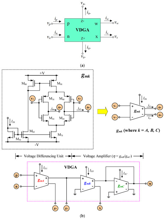
Figure 1.
Voltage differencing gain amplifier (VDGA). (a) Circuit representation; (b) CMOS realization.
Here, gmk (where k = A, B, C) and η are the transconductance gain and the transfer voltage gain of the VDGA, respectively. Generally, the gmk value is electronically tunable via an external bias current, simplifying the design of circuit parameters. Electronic control becomes crucial when circuit design parameters are altered and the integrated circuit is constructed. According to the CMOS VDGA circuit in Figure 1b, the voltage gain η is equal to the ratio of gmB to gmC (or η = gmB/gmC).
3. Proposed Resistorless Mixed-Mode Universal Filter
Figure 2 illustrates the proposed mixed-mode universal biquadratic filter, which is designed using two VDGA units and two grounded capacitors, eliminating the need for any external passive resistors. In IC design, employing grounded capacitors is helpful for reducing stray parasitic capacitance at their terminals, which is alleviated by external grounded capacitors.
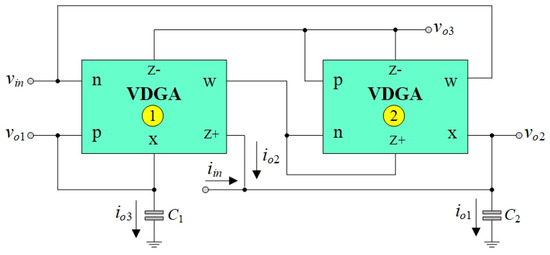
Figure 2.
Proposed resistorless mixed-mode universal biquad filter.
With the same designed topology, the proposed circuit can realize mixed-mode universal filter functions in VM, TAM, CM, and TIM, as characterized below.
3.1. VM Filter
If iin = 0, namely open-circuited, the electronically tunable SITO universal filter in VM can be obtained with the following voltage transfer functions:
and
In the above relations, the transfer functions TLP(s), TBP(s), and THP(s) are in the form of, respectively:
and
where:
In the expressions above, the parameters gmki and ηi (i = 1, 2) refer to the gains gmk and η of the corresponding VDGA. As indicated by Equations (2)–(4), the output voltage vo1 exhibits a noninverting LP response, vo2 displays an inverting BP response, and vo3 presents an inverting HP response. In addition to Equation (7), the realization of the HP filter requires an equal element condition gmA2 = gmB2.
3.2. TAM Filter
With iin = 0, the BP and HP filter responses in TAM can also be realized from io2 and io3, respectively, as given by:
and
The proposed circuit realizes TAM BP and HP filter functions, as shown in Equations (9) and (10), with the passband gains of (gmB1/gmA1) and (gmA2/gmA1), respectively. Note that the passband gains for the proposed circuit can be tuned electronically by adjusting the ratio of VDGA transconductances. It is important to mention that the output current responses of this type are sensed from the passive elements; therefore, the practical implementations necessitate the current sensing units. The works of [4,19,23] suggested innovative solutions to achieving high-output impedance.
3.3. CM Filter
If vin = 0, namely the node vin is connected to ground, three generic biquadratic filter functions in CM may be derived simultaneously, and its transfer functions can be expressed by the following:
and
It is further noted that the BS current response can be realized by connecting the relevant output currents as follows: iBS = io3 + io1. Similarly, the AP current response can be derived from the interconnection of LP, BP, and HP responses, expressed as iAP = io3 + io2 + io1. Since the LP current response io1 exhibits an inverting phase, an additional element is necessary to provide the noninverting phase of io1 for the BS and AP filter functions.
3.4. TIM Filter
With vin = 0, the following LP, BP, and HP filter response in TIM can be obtained at the output terminals vo1, vo2, and vo3, respectively:
and
The realized filtering functions demonstrate that the circuit can generate all three standard biquadratic filter functions in all four operational modes utilizing the same circuit design. Thus, the circuit depicted in Figure 2 operates as a mixed-mode universal biquad filter, featuring the following key parameters:
and
where η1 = gmB1/gmC1, ωp is the pole frequency in radians/second and Q is the quality factor of the filter. Equation (17) indicates that the circuit possesses electronic adjustability of the frequency ωp through gmA1 and/or gmB1. On the other hand, the parameter Q in Equation (18) can also be electronically and independently tuned without affecting ωp by gmB2 and/or gmC1. Consequently, the parameters ωp and Q are orthogonally tunable by controlling (gmA1 and/or gmB1) and (gmB2 and/or gmC1) in that order. This feature is desired in universal biquadratic filters to provide flexibility of designing and tuning. Table 2 provides the passband gains for the proposed filter functioning in all four modes.
Table 2.
Passband gains of the proposed mixed-mode universal biquad filter in Figure 2.
4. Proposed Resistorless Dual-Mode Quadrature Oscillator
The proposed resistorless dual-mode QO circuit is slightly modified from Figure 2 by removing both input signals vin and iin, as illustrated in Figure 3. Circuit analysis of the configuration shown in Figure 3 leads to the following characteristic equation:
where η2 = gmB2/gmC2.
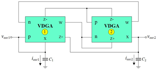
Figure 3.
Proposed resistorless dual-mode quadrature oscillator.
From Equation (19), the oscillation condition (OC) and the oscillation frequency (ωosc) of the proposed dual-mode QO can be derived, respectively, as:
and
Equation (20) shows that the OC may be electrically modulated via gmC2 without influencing the ωosc. It should also be noted that the ωosc in Equation (21) can be independently adjusted by gmA1 and/or gmB1. In other words, both OC and ωosc parameters can be electronically and separately regulated by the selection of separate transconductances.
In a sinusoidal steady state, two output voltages vosc1 and vosc2 of the oscillator have the following relationship:
This implies that the two voltage outputs are phase-shifted by 90°. Consequently, we expect that the output voltages vosc1 and vosc2 will be in quadrature form.
In the same way, the output currents iosc1 and iosc2 in the sinusoidal steady state exhibit a similar relationship as:
Consequently, the output currents are quadrature signals as well.
5. Finite Tracking Error Analysis
The finite tracking signal errors associated with the VDGA terminals may be taken into account in practical performance. By considering the parasitic transfer gains, we can describe the realistic VDGA using the following relationships:
In this case, αk (αk = 1 − εα) denotes the nonideal transconductance gain, while δ (δ = 1 − εδ) indicates the nonideal voltage gain. Both deviate from their optimal values due to the transfer errors εα (|εα | << 1) and εδ (|εδ | << 1).
The suggested resistorless mixed-mode universal biquad filter circuit depicted in Figure 2 is examined utilizing the nonideal model (24) of VDGA, resulting in the modified values ωp and Q as follows:
and
where αAi, αBi, and δi are the nonideal gains αA, αB, and δ of the i-th VDGA (i = 1, 2), respectively. From Equations (25) and (26), the various sensitivity coefficients with respect to active and passive elements are determined as:
and
Further, from Figure 3, the impact of the finite tracking signal errors on the OC and ωosc can then be obtained as:
and
From Equation (31), we find that the active and passive sensitivities of the ω′osc for the proposed dual-mode QO circuit depicted in Figure 3 are identical to those expressed in Equation (27).
6. Parasitic Impedance Effect Analysis
The next nonlinear consideration is the effects of the VDGA parasitic impedances on the circuit performance. Figure 4 shows the practical behavior model of the VDGA, including corresponding terminal parasitics [30]. The real VDGA possesses high-impedance parallel parasitic elements (Rp//Cp), (Rn//Cn), (Rz+//Cz+), (Rz−//Cz−), and (Rx//Cx) at the respective ports p, n, z+, z−, and x, together with a small serial parasitic resistance Rw at port w. Taking these parasitics into account, the nonideal values of ωp and Q for the proposed mixed-mode universal biquad filter depicted in Figure 2 are modified as follows:
and
where R′1 = (Rp1//Rx1), C′1 = C1 + Cp1 + Cx1, and C′2 = C2 + Cz2+ + Cx2. Since it is known that R′1 >> 1, the values of the external capacitors C1 and C2 should be designated as Equation (34) to avoid the parasitic effects shown in Figure 4.
C1 >> Cp1 + Cx1 and C2 >> Cz2+ + Cx2,
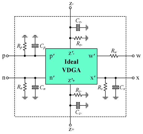
Figure 4.
Practical behavior model of the VDGA with its parasitic impedances.
Likewise, if the proposed dual-mode QO circuit in Figure 3 is evaluated in the presence of parasitics, the nonideal OC and ωosc may be derived as follows:
and
7. Simulation Verification
The practicality of the proposed circuits in Figure 2 and Figure 3 has been evaluated by PSPICE simulation using CMOS VDGA, shown in Figure 1b [30], whereas 0.18 μm CMOS technology from TSMC was employed. In the simulation, the aspect ratios W/L (in μm/μm) of different CMOS transistors are as follows: M1k − M2k = 24/0.18, M3k − M4k = 30/0.18, M5k − M7k = 5/0.18, and M8k − M9k = 6/0.18. They were supplied with DC voltages of ±0.9 V. The CMOS VDGA circuit in Figure 1b gives the relationship between the transconductance gain gmk and the corresponding bias current IBk, which can be written as [29]:
where:
and μ is the carrier mobility, Cox is the gate-oxide capacitance per unit area, and Wj/Lj is the aspect ratio of transistor Mjk, respectively.
7.1. Simulation Results of the Proposed Mixed-Mode Universal Biquad Filter in Figure 2
The proposed resistorless mixed-mode universal biquad filter in Figure 2 was designed for the following frequency specifications: fp = 1.59 MHz and Q = 1. The specified filter parameters yield component values of gmAi = gmBi = gmCi = 1 mA/V (i = 1, 2) and C1 = C2 = 100 pF.
Figure 5 and Figure 6, respectively, illustrate the simulation results of the time-domain and frequency-domain responses in VM and CM. A sinusoidal input signal with a peak amplitude of 40 mV at 1.59 MHz was applied to the proposed filter during time-domain response study. Similarly, Figure 7 and Figure 8 present the simulated frequency characteristics for the TIM and TAM filters, respectively. There is significant agreement between the theory and simulation values. Additionally, the total power consumption of the circuit was determined to be 2.84 mW.
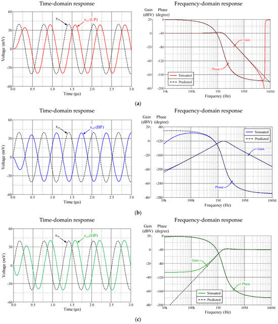
Figure 5.
Simulation results of the proposed VM filter in Figure 2. (a) LP; (b) BP; (c) HP.
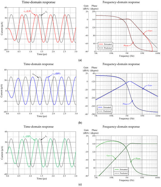
Figure 6.
Simulation results of the proposed CM filter in Figure 2. (a) LP; (b) BP; (c) HP.
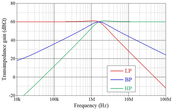
Figure 7.
Simulated frequency responses of the proposed TIM filter in Figure 2.
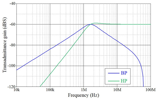
Figure 8.
Simulated frequency responses of the proposed TAM filter in Figure 2.
To demonstrate the electronic tunability of the proposed universal filter illustrated in Figure 2, the frequency responses of the VM BP filter for various pole frequencies fp are plotted in Figure 9. To achieve this, the frequency fp was adjusted for three different values, i.e., fp = 0.62 MHz, 1.01 MHz, and 1.59 MHz, by changing the gmki value to 0.39 mA/V, 0.63 mA/V, and 1 mA/V, respectively. The findings indicated that the simulated fp values were 0.616 MHz, 1.07 MHz, and 1.585 MHz, which correspond to the percentage absolute errors of 0.64%, 5.90%, and 0.31%, respectively. Figure 10 depicts the simulated frequency responses of the VM BP filter for various Q-values. Table 3 tabulates the values of the active component corresponding to different Q-values based on the designs. The proposed circuit facilitates independent electronic adjustment of the fp and Q values, as seen in Figure 9 and Figure 10.
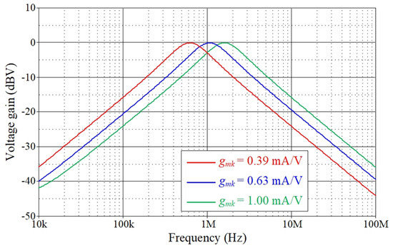
Figure 9.
Simulated frequency responses of the VM BP filter in Figure 2 with tuning fp value.
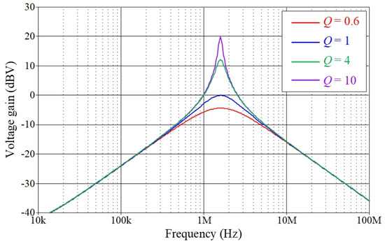
Figure 10.
Simulated frequency responses of the VM BP filter in Figure 2 with tuning Q value.
Table 3.
Active component values of the proposed VM BP filter for tuning Q values at fp = 1.59 MHz (gmA1 = gmA2 = gmB2 = gmC2 = 1 mA/V).
Additionally, the sensitivity performance was examined for 100 runs using Monte Carlo statistical analysis, which considers both transconductances (gmki) and capacitance values (C1 and C2) with a 5% variation. Figure 11 shows the generated family histograms of fp. The mean and standard deviation were 1.63 MHz and 53.74 kHz, respectively, demonstrating that the scheme possesses sufficient sensitivity.
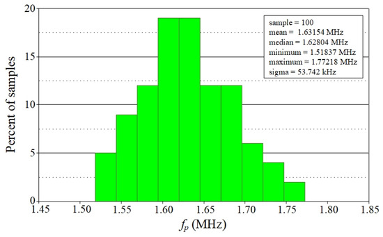
Figure 11.
Monte Carlo statistical analysis results of the VM BP response with 5% deviation in transconductance and capacitor values.
Furthermore, to demonstrate the robustness of the proposed universal filter in Figure 2, the pole frequency fp is analyzed at different process corner, voltage, and temperature (PVT) variations. Figure 12 presents the simulation results for the fp of the VM BP filter response under PVT variations. The process corners were selected for the parameters nominal–nominal (NN), slow–slow (SS), fast–fast (FF), slow–fast (SF), and fast–slow (FS). We observe that the fp increases as the supply voltage increases. As the temperature increases, the operating transistor current decreases, leading to a decrease in fp. As a result, power dissipation diminishes up to a specific temperature. In both cases, the fp of the proposed universal filter was varied by variations in temperature and voltage, as it is contingent upon the device current of the transistor.
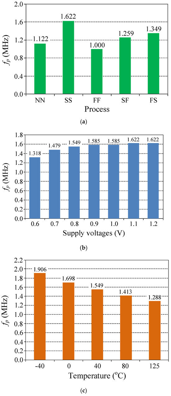
Figure 12.
Simulation results for the PVT variation. (a) Process variation; (b) supply voltage variation; (c) temperature variation.
7.2. Simulation Results of the Proposed Dual-Mode Quadrature Oscillator in Figure 3
The VM quadrature sinusoidal output waveforms of the proposed resistorless dual-mode QO circuit in Figure 3, with gmki = 1 mA/V and C1 = C2 = 100 pF, are shown in Figure 13. The circuit was designed to oscillate at a frequency of fosc = 1.59 MHz. The simulated frequency of oscillation was recorded at 1.58 MHz, exhibiting a phase difference of 92.85° between the quadrature outputs. Figure 14 displays the corresponding Lissajous plot (x-y mode) between vosc1 and vosc2. The total harmonic distortion analysis of vosc1 is also derived, yielding a value of approximately 1.89%. An additional pertinent concern is the phase noise performance of the oscillator. As the next step, the phase noise of both outputs, vosc1 and vosc2, is determined, and the obtained results are plotted in Figure 15. Table 4 provides the phase noise performance data evaluated at various relative frequencies.
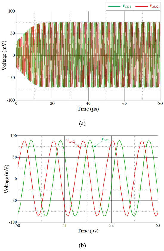
Figure 13.
Simulation results for vosc1 and vosc2 of the proposed dual-mode QO circuit in Figure 3. (a) Initial state; (b) steady state.
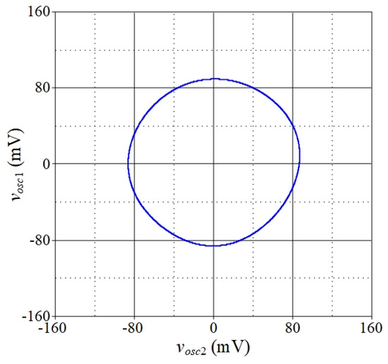
Figure 14.
Simulated Lissajous plot between vosc1 and vosc2.
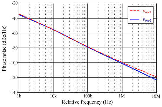
Table 4.
Phase noise performance of the proposed QO circuit evaluated at various frequencies.
Furthermore, Figure 16 illustrates the simulated quadrature output waveforms of iosc1 and iosc2 in Figure 3. Note that the waveform appears visibly mismatched in both amplitude and symmetry. These asymmetries could indeed stem from the differences in the VDGA implementation shown in Figure 3 and the biasing between the two signal paths. To address this issue, the layout-level symmetry or tuning mechanisms should consider and potentially incorporate phase and amplitude error metrics. The electronic tunability of both calculated and simulated fosc is plotted in Figure 17, with changing gmB1 value while keeping gmA1 constant at 1 mA/V. According to Figure 17, the useful fosc ranges from roughly 750 kHz to 1.87 MHz.
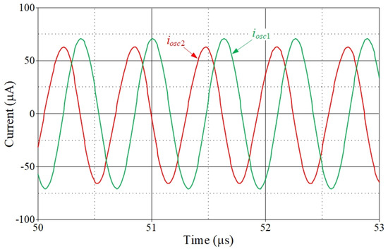
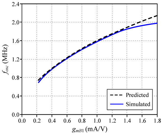
Figure 17.
Electronic controllability of fosc as a function of gmB1.
8. Experimental Verification
The proposed circuits in Figure 2 and Figure 3 were experimentally confirmed to support the theoretical hypotheses. As conceptually illustrated in Figure 18, the VDGA was performed using practical measurements with commonly utilized IC-type LM13600 dual operational transconductance amplifiers (OTAs) from National Semiconductor company, USA [31]. The power supply voltages were employed as ±5 V.
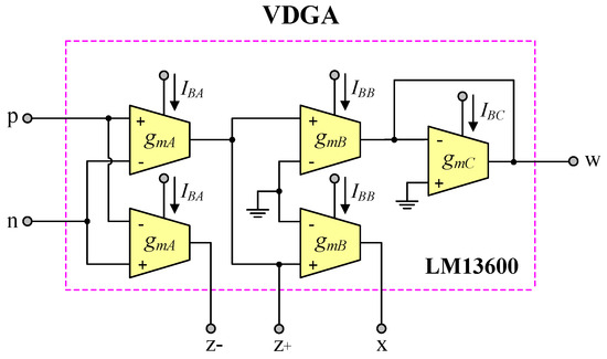
Figure 18.
Practical implementation of VDGA in experimental measurement testing.
8.1. Experimental Results of the Proposed Mixed-Mode Universal Biquad Filter in Figure 2
The active and passive component values of Figure 2 were designated as gmki = 0.8 mA/V (for IBki = 42 μA) and C1 = C2 = 2 nF, corresponding to the theoretical values of fp = 63.66 kHz and Q = 1. Figure 19, Figure 20 and Figure 21 show the measured time-domain responses and their corresponding frequency spectrums for the LP, BP, and HP filters in VM. The signal input voltage (vin) for time-response measurements was set to 50 mV (peak) at a frequency of 63.66 kHz. The recorded fp in the measured LP and BP voltage response of Figure 19 and Figure 20 was 63.80 kHz, which is a −0.22% deviation from the ideal value. In the HP voltage response of Figure 21, the measured fp is 63.10 kHz, reflecting a deviation of +0.88% from the predicted value. Figure 22 represents the experimental frequency responses for the LP, BP, and HP voltage responses of Figure 2. The results indeed show that the measured BP and HP responses at low frequencies reach only about −10 dB in their stopbands, which is unusually low and not characteristic of ideal filter behavior. This indicates a significant parasitic effect: a fraction of the LP response term contaminates the BP and HP numerators. Such contamination mainly could occur due to parasitic capacitances within the integrated circuit layout and incomplete pole-zero cancellation in the signal path caused by mismatches. This contamination leads to a partial addition of the low-frequency gain from the LP function into the BP and HP outputs, which should ideally have attenuated these components significantly more deeply—on the order of −40 dB or lower. As also noted in [31], the gain-bandwidth product (GBP) of the IC LM13600 used in experiments is around 2 MHz. As a result, the discrepancies in gain for the measured high-frequency HP and BP responses arise mainly from GBP effects of the IC LM13600 OTAs. Nevertheless, the use of high-speed IC devices extends the useful frequency of the proposed circuit.
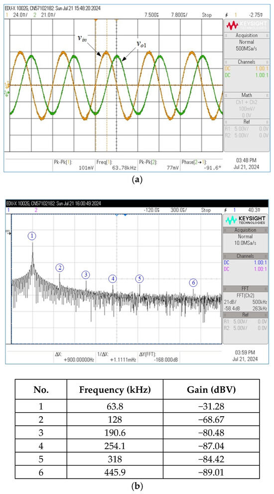
Figure 19.
Experimentally measured responses of the LP filter in VM. (a) Time-domain responses; (b) frequency spectrum.
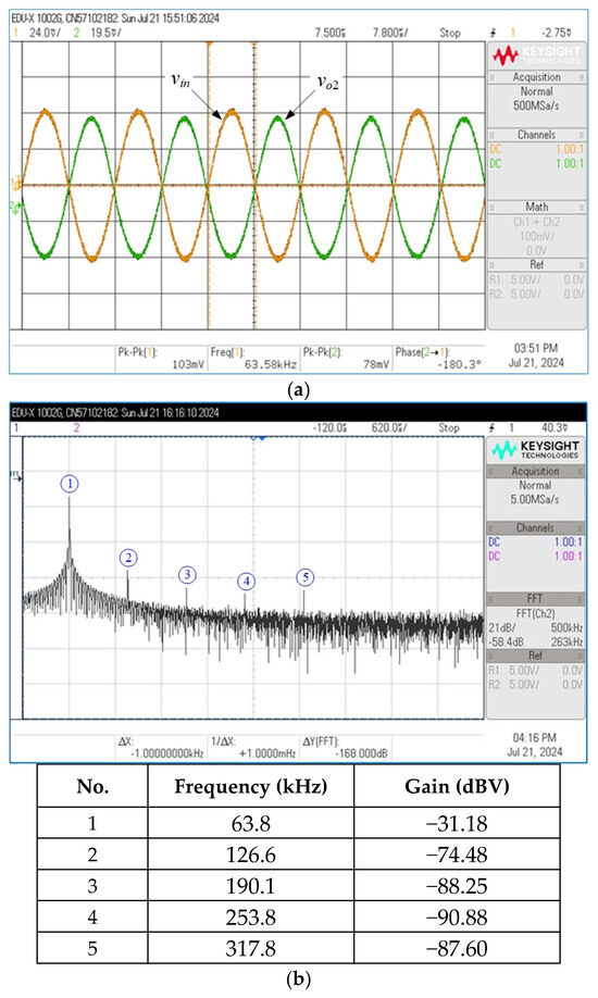
Figure 20.
Experimentally measured responses of the BP filter in VM. (a) Time-domain responses; (b) frequency spectrum.
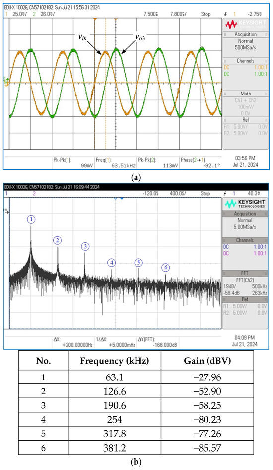
Figure 21.
Experimentally measured responses of the HP filter in VM. (a) Time-domain responses; (b) frequency spectrum.
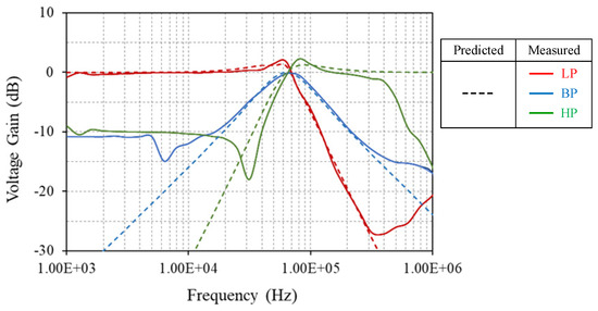
Figure 22.
Experimental frequency responses for the LP, BP, and HP voltage responses in Figure 2.
8.2. Experimental Results of the Proposed Dual-Mode Quadrature Oscillator in Figure 3
The VDGA-based resistorless dual-mode QO circuit in Figure 3 was designed to achieve an oscillation frequency of fosc = 63.66 kHz. As per Equation (21), the designed component values for C1 = C2 = 2 nF yielded gmki = 0.8 mA/V. Figure 23 shows the measured transient waveforms for the quadrature voltage outputs vosc1 and vosc2. It is observed that the quadrature oscillation outputs exhibit a 92.8° phase difference. The Lissajous figure of the two output voltages is shown in Figure 24 to determine the correlation between the quadrature outputs. Figure 25 further illustrates the corresponding spectrum frequency of vosc1, revealing that the practical fosc was around 63 kHz, with a percentage error of 1.04% and a gain of −33.20 dBV.
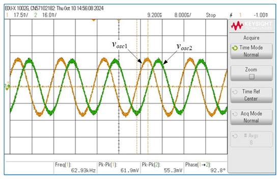
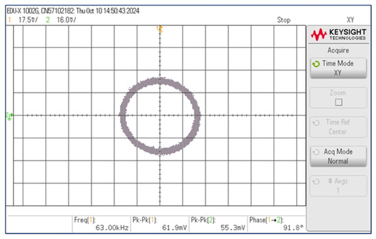
Figure 24.
Measured Lissajous plot between vosc1 and vosc2.
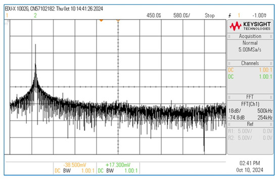
Figure 25.
Experimental frequency spectrum of vosc1 in Figure 3.
9. Comparison with the Prior Similar Circuits
This study introduces a simple structure for a biquadratic filter and quadrature oscillator circuit, designed without resistors and using only two grounded capacitors. The proposed filter circuit can operate in four modes: VM, TAM, CM, and TIM, with its important parameters electronically adjustable via the transconductance gain (gm). Meanwhile, the proposed oscillator circuit can generate two modes of sinusoidal signals: VM and CM.
Based on the comparison in Table 1, it is evident that most of the articles present either a filter or an oscillator circuit. In contrast, the works of [3,8,13,14,19,20,24,25] are capable of filtering the signal and generating a sine wave. While some oscillator circuits in [8,13,19,24] can produce both VM and CM signals, it is noted that, in [8,19], the filter circuit operates in only one mode. Only the filters in [13,24] can function in two modes, VM and CM. Despite the lack of a resistor in [24], the circuit of [13] requires both grounded and floating resistors in [13]. In addition, both articles use computer simulation to verify circuit operations. Neither article conducts experimental circuit testing.
Consequently, the design proposed in this study provides significant features and practical advantages in terms of flexibility, space saving, and ease of integration with commercial ICs.
10. Conclusions
This study proposes a VDGA-based electrically tunable resistorless mixed-mode universal filter, utilizing only two grounded capacitors and eliminating the requirement for external passive resistors. The proposed filter circuit is capable of implementing all general biquadratic filter functions across the four operational modes: VM, TAM, CM, and TIM. The pole frequency and quality factor of the implemented filter can be altered electronically and independently by changing the transconductance gains of the VDGA. The suggested filter circuit can be modified to operate as a dual-mode quadrature oscillator, producing both voltage and current output from a single configuration. An examination of the nonideal circuit performance has been conducted. The practical feasibility of the circuit has been validated using PSPICE computational results and experimental tests.
Author Contributions
Conceptualization, O.C., J.T., T.P. and W.T.; methodology, O.C., J.T., T.P. and W.T.; software, O.C. and J.T.; validation, O.C., J.T., T.P. and W.T.; formal analysis, T.P. and W.T.; investigation, O.C., J.T. and W.T.; resources, T.P. and W.T.; data curation, T.P. and W.T.; writing—original draft preparation, O.C. and J.T.; writing—review and editing, T.P. and W.T.; visualization, O.C., J.T. and W.T.; supervision, T.P. and W.T.; project administration, T.P.; funding acquisition, O.C., J.T. and W.T. All authors have read and agreed to the published version of the manuscript.
Funding
This research project is supported by Rajamangala University of Technology Isan, Contract No. ENG7/67.
Institutional Review Board Statement
Not applicable.
Informed Consent Statement
Not applicable.
Data Availability Statement
The original contributions presented in the study are included in the article, further inquiries can be directed to the corresponding author.
Acknowledgments
The authors appreciate the support and infrastructure provided by the School of Engineering, King Mongkut’s Institute of Technology Ladkrabang, for the completion of this work.
Conflicts of Interest
The authors declare no conflicts of interest.
References
- Chen, H.P.; Hwang, Y.S.; Ku, Y.T.; Lin, T.J. Voltage-mode biquadratic filters using single DDCCTA. Int. J. Electron. Commun. (AEU) 2016, 70, 1403–1411. [Google Scholar] [CrossRef]
- Horng, J.W.; Chiu, W.Y. High input impedance voltage-mode biquad with one input and five outputs employing four CCII ICs. Indian J. Pure Appl. Phys. 2016, 54, 577–582. [Google Scholar]
- Tuntrakool, S.; Kumngern, M.; Sotner, R.; Herencsar, N.; Suwanjan, P.; Jaikla, W. High input impedance voltage-mode universal filter and its modification as quadrature oscillator using VDDDAs. Indian. J. Pure Appl. Phys. 2017, 55, 324–332. [Google Scholar]
- Gupta, M. New single input multiple output type current mode biquad filter using OTAs. Circuits Syst. 2016, 7, 231–238. [Google Scholar] [CrossRef]
- Pandey, R.; Pandey, N.; Singhal, N. Single VDTA based dual mode single input multioutput biquad filter. J. Eng. 2016, 2016, 1674343. [Google Scholar] [CrossRef]
- Kumngern, M.; Khateb, F.; Kulej, T.; Kyselak, M.; Lerkvaranyu, S.; Knobnob, B. Current-mode shadow filter with single-input multiple-output using current-controlled current conveyors with controlled current gain. Sensors 2024, 24, 460. [Google Scholar] [CrossRef] [PubMed]
- Kumngern, M. One-input three-output current-mode universal filter using translinear current conveyors. Int. J. Inf. Technol. Electr. Eng. 2018, 2, 101–106. [Google Scholar] [CrossRef]
- Kumar, A.; Chaturvedi, B. Novel CMOS dual-X current conveyor transconductance amplifier realization with current-mode multifunction filter and quadrature oscillator. Circuits Syst. Signal Process. 2018, 37, 2250–2277. [Google Scholar] [CrossRef]
- Mohan, J.; Chaturvedi, B.; Kumar, A.; Jitender. SIMO type voltage-mode biquadratic multifunction filter. In Proceedings of the 6th International Conference on Signal Processing and Integrated Networks (SPIN), Noida, India, 7–8 March 2019; pp. 478–482. [Google Scholar]
- Huaihongthong, P.; Chaichana, A.; Suwanjan, P.; Siripongdee, S.; Sunthonkanokpong, W.; Supavarasuwat, P.; Jaikla, W.; Khateb, F. Single-input multiple-output voltage-mode shadow filter based on VDDDAs. Int. J. Electron. Commun. (AEU) 2019, 103, 13–23. [Google Scholar] [CrossRef]
- Alpaslan, H.; Yuce, E. DVCC+ based multifunction and universal filters with the high input impedance features. Analog. Integr. Circuits Signal Process. 2020, 103, 325–335. [Google Scholar] [CrossRef]
- Choraria, K.; Divya; Basson, I.; Pandey, R. CDTA based multimode SIMO biquad filter. In Proceedings of the 2020 International Conference on Communication and Signal Processing (ICCSP), Chennai, India, 28–30 July 2020; pp. 0661–0666. [Google Scholar]
- Tangsrirat, W.; Pukkalanun, T.; Channumsin, O. Single VDGA-based dual-mode multifunction biquadratic filter and quadrature sinusoidal oscillator. Inf. MIDEM 2020, 50, 125–136. [Google Scholar]
- Wang, S.F.; Chen, H.P.; Ku, Y.; Zhong, M.X. Voltage-mode multifunction biquad filter and its application as fully-uncoupled quadrature oscillator based on current-feedback operational amplifiers. Sensors 2020, 20, 6681. [Google Scholar] [CrossRef]
- Wai, M.P.P.; Suwanjan, P.; Jaikla, W.; Chaichana, A. Electronically and orthogonally tunable SITO voltage-mode multifunction biquad filter using LT1228s. Elektron. Elektrotechnika 2021, 27, 2962–2973. [Google Scholar] [CrossRef]
- Güney, A.; Kacar, F.; Kuntman, H. CMOS realization of electronically tunable VDCC based single-input-dual-output filter. Int. J. Electron. Commun. (AEU) 2021, 139, 153627. [Google Scholar] [CrossRef]
- Wang, S.F.; Chen, H.P.; Ku, Y.; Li, Y.F. High-input impedance voltage-mode multifunction filter. Appl. Sci. 2021, 11, 387. [Google Scholar] [CrossRef]
- Wai, M.P.P.; Chaichana, A.; Jaikla, W.; Siripongdee, S.; Suwanjan, P. One input voltage and three output voltage universal biquad filters with orthogonal tune of frequency and bandwidth. Int. J. Electr. Comput. Eng. 2021, 11, 2962–2973. [Google Scholar]
- Arora, T.S. A current mode universal filter and a single resistance controlled oscillator employing only grounded passive elements: Applications of VDCC. Electronics 2021, 25, 65–76. [Google Scholar] [CrossRef]
- Jaikla, W.; Siripongdee, S.; Khateb, F.; Sotner, R.; Silapan, P.; Suwanjan, P.; Chaichana, A. Synthesis of biquad filters using two VD-DIBAs with independent control of quality factor and natural frequency. Int. J. Electron. Commun. (AEU) 2021, 132, 153601. [Google Scholar] [CrossRef]
- Roongmuanpha, N.; Faseehuddin, M.; Herencsar, N.; Tangsrirat, W. Tunable mixed-mode voltage differencing buffered amplifier-based universal filter with independently high-Q factor controllability. Appl. Sci. 2021, 11, 9606. [Google Scholar] [CrossRef]
- Unuk, T.; Yuce, E. A mixed-mode filter with DVCCs and grounded passive components only. Int. J. Electron. Commun. (AEU) 2022, 144, 153063. [Google Scholar] [CrossRef]
- Pandey, Y.; Arora, T.S. A current-mode active filter using VDCCs and only grounded passive elements. In Proceedings of the 2022 2nd International Conference on Emerging Frontiers in Electrical and Electronic Technologies (ICEFEET), Patna, India, 24–25 June 2022. [Google Scholar]
- Tangsrirat, W.; Channumsin, O.; Unhavanich, S.; Pukkalanuna, T. Dual-mode single-input three-output multifunction filter and quadrature oscillator consisting of two voltage differencing transconductance amplifiers and two grounded capacitors. J. Commun. Technol. Electron. 2023, 68, 460–473. [Google Scholar] [CrossRef]
- Chen, H.P.; Wang, S.F.; Ku, Y.; Yi, Y.C.; Chen, Y.H. Experimental verification of on-chip biquadratic filter and oscillator. IEEE Sens. J. 2023, 23, 3736–3746. [Google Scholar] [CrossRef]
- Nakoa, J.; Psychalinosa, C.; Minaei, S. Single-input multiple-output inverse filter designs with cascade capability. Int. J. Electron. Commun. (AEU) 2024, 175, 155061. [Google Scholar] [CrossRef]
- Singh, S.; Garima; Jaint, B. Dual mode SIMO biquad filter using VDTA. In Proceedings of the 2024 International Conference on Electronics, Computing, Communication and Control Technology (ICECCC), Bengaluru, India, 2–3 May 2024. [Google Scholar]
- Wai, M.P.P.; Jaikla, W.; Chaichana, A.; Chanapromma, C.; Suwanjan, P.; Sunthonkanokpong, W. Voltage-mode biquad filter using three LT1228s with independent and electronic control of center frequency and quality factor. Eng. Lett. 2023, 31, 681–688. [Google Scholar]
- Satansup, J.; Tangsrirat, W. CMOS realization of voltage differencing gain amplifier (VDGA) and its application to biquad filter. Indian. J. Eng. Mater. Sci. 2013, 20, 457–464. [Google Scholar]
- Roongmuanpha, N.; Tangsrirat, W.; Pukkalanun, T. Single VDGA-based mixed-mode universal filter and dual-mode quadrature oscillator. Sensors 2022, 22, 5303. [Google Scholar] [CrossRef]
- National Semiconductor. LM13600: Dual Operational Transconductance Amplifiers with Linearizing Diodes and Buffers. Available online: https://pdf1.alldatasheet.com/datasheet-pdf/view/8640/NSC/LM13600N.html (accessed on 12 December 2024).
Disclaimer/Publisher’s Note: The statements, opinions and data contained in all publications are solely those of the individual author(s) and contributor(s) and not of MDPI and/or the editor(s). MDPI and/or the editor(s) disclaim responsibility for any injury to people or property resulting from any ideas, methods, instructions or products referred to in the content. |
© 2025 by the authors. Licensee MDPI, Basel, Switzerland. This article is an open access article distributed under the terms and conditions of the Creative Commons Attribution (CC BY) license (https://creativecommons.org/licenses/by/4.0/).