Abstract
In this study, various factors affecting the efficiency of the MAPbI3 perovskite solar cell (PSC) were analyzed using the SCAPS-1D simulation program. The basic device analyzed in this study had a structure of ITO/TiO2/MAPbI3/Cu2O/Au. The thickness of each layer (electron transport layer (ETL), perovskite absorption layer (PAL), and hole transport layer (HTL)), PAL defect density and interface defect density were investigated as parameters. The optimized parameters that yielded the highest light conversion efficiency were an ETL (TiO2) thickness of 100 nm, a PAL (MAPbI3) thickness of 1300 nm, an HTL (Cu2O) thickness of 400 nm, a PAL defect density of 1014 cm−3, and an interface defect density of 1013 cm−3 for both absorber/ETL and absorber/HTL interfaces. The optimized PSC exhibited a maximum efficiency of 19.30%. These results obtained in this study are expected to contribute considerably to the optimization and efficiency improvement of perovskite solar cells using inorganic charge-carrier transport layers.
1. Introduction
Organic–inorganic perovskites have recently attracted considerable attention as absorbers in solar cells; they have a chemical formula of ABX3 and have a three-dimensional structure with organic cations, such as CH3NH3, CH(NH2)2, Cs, and Rb at A, cations such as Pb, Sn, and Ge at B, and halogen anions such as I, Br, Cl, and F at X [1,2]. Perovskites exhibit different performances and properties in solar cells depending on their constituent elements [3]. Since the first study on CH3NH3PbX3 perovskites in 2009, their efficiency has considerably improved to 25.7% or more, resulting in the maximum power conversion efficiency (PCE) [4,5,6,7,8]. Representative perovskites include CH3NHPbI3 (MAPbI3) and CH(NH2)2PbI3 (FAPbI3). The advantages of perovskites include the possibility of a low-cost production through a low-temperature solution process and a high efficiency because of a high light-absorption coefficient [9]. However, some issues need to be solved; in particular, Pb is harmful to the environment; thus, Pb-free materials should be developed [10].
In addition, existing structures using organic materials for the common layers, Electron Transport Layer (ETL) and Hole Transport Layer (HTL), are sensitive to moisture [11,12]. Therefore, in order to overcome these disadvantages, research on using inorganic materials instead of organic materials for common layers such as ETL and HTL is being actively conducted [13].
Among the widely studied inorganic Electron Transport Layers (ETL) and Hole Transport Layers (HTL) in the device structure of perovskite solar cells (PSCs), looking first at ETL materials, substances such as SnO2, ZnO, and TiO2, which exhibit n-type semiconductor characteristics, are commonly utilized [14,15].
SnO2 is one of the most widely researched transparent conducting oxides (TCOs) as a transparent electrode since the early days of TCOs research, due to its transparent properties and high conductivity [16]. Furthermore, by controlling oxygen deficiency, its electrical characteristics can be adjusted from conducting to semiconductor, enabling extensive application research on thin film transistors as channel layers [17]. In particular, significant research has been conducted to control the electrical properties and improve reliability by doping SnO2 with other materials, such as Al, In, Ta, etc. [18,19,20].
Additionally, ZnO is one of the most abundant materials on earth and is currently being evaluated in various multi-layer device structures as an Electron Transport Layer (ETL) material in perovskite solar cells. ZnO has a wide bandgap energy (Eg = 3.26 eV) and excellent mobility [21]. With its wide bandgap and significant exciton binding energy, ZnO is considered one of the most interesting ETL materials [22]. In particular, there has been active research in doping with various other materials to create p-type ZnO [23,24]. However, a reliable p-type ZnO has not yet been reported [25]. Nonetheless, in the case of IGZO (a mixture of In2O3, Ga2O3, and ZnO), although it exhibits n-type characteristics, it is commercially utilized as the channel layer of the thin film transistor (TFT) in large organic light-emitting devices, due to its reliability under operating voltage and current conditions [26,27].
TiO2 is the most researched material for the electron transport layer in the multi-layer structure of perovskite solar cells. This preference is due to TiO2’s high chemical and optical stability, non-toxicity, and low cost, making it well-suited for applications in the optical field [28,29]. Among TiO2 structures, anatase is preferred in the photovoltaic field due to its higher conduction band edge energy and lower electron–hole recombination rate [30]. These various excellent properties led to the selection of TiO2 as the ETL material in this study.
In addition, p-type inorganic semiconductor materials that can serve as a hole transport layer (HTL) include MoO3, CuI, NiOx and Cu2O [31,32,33]. MoO3 has a wide bandgap, typically around 3.0 eV, which contributes to its transparency in the visible part of the spectrum [34]. This makes it useful in applications requiring transparent conducting layers, as well as in optoelectronic devices where light absorption or transmission is critical. Also, MoO3 has a high work function, which makes it an excellent hole-injection layer in organic electronic devices [35]. This property facilitates the efficient transfer of holes from the anode to the organic layer in organic-emitting diodes (OLEDs) and organic photovoltaics (OPVs). Copper Iodide (CuI) is another p-type inorganic semiconductor material known for its distinctive properties that make it suitable for a range of electronic and optoelectronic applications [36]. CuI has a direct bandgap that is typically reported to be around 3.1 eV, making it transparent to visible light [37]. One of the significant advantages of CuI is its relatively high hole mobility compared to other p-type semiconductors [38]. CuI is chemically stable under a wide range of conditions and can be easily doped with various elements to fine-tune its electrical and optical properties [39].
P-type NiOx demonstrates a significant bandgap (greater than 3.5 eV) coupled with exceptional transparency within the visible spectrum [40]. This characteristic effectively reduces losses, including charge recombination, improves charge transport, and ensures ideal energy level alignment with diverse photoactive absorbers, attributed to its adequate conductivity and chemical stability [41,42,43]. These properties have led to extensive research on using these materials as hole injection layers or hole transfer layers in Quantum-Organic Light Emitting Diodes (QLED) device structures [44,45].
In this paper, Cu2O was selected as the hole transport layer (HTL) material. Because Cu2O has a low bandgap energy of 1.8~2.5 eV, the efficient conversion of light into electrical energy is possible, and it has a high hole mobility, enabling the photovoltaic solar cell efficiency to be improved [46,47]. Furthermore, Cu2O is a stable material and does not undergo significant changes in its electronic properties, even under harsh conditions, and it is a non-toxic and environmentally friendly material, making it a desirable choice for applications in the fields of energy and environment [48,49]. Therefore, in this study, TiO2 and Cu2O were selected as the ETL and HTL materials, respectively, based on these excellent characteristics and the band alignment of the energy band diagram. In summary, this study optimized the power conversion efficiency (PCE) of perovskite solar cells using TiO2 as an Electron Transport Layer (ETL), MAPbI3 as an absorber layer, and Cu2O as a Hole Transport Layer (HTL), respectively.
We analyzed the effects of the following parameters on the power conversion efficiency (PCE) of perovskite solar cells (PSCs) through parameters optimization via the SCAPS-1D simulation tool [50,51]: HTL thickness, perovskite absorber layer (PAL) thickness, ETL thickness, the defect density in the perovskite absorber layer (PAL), the defect density at the interface between the absorber and electron transport layers (ETLs), and that between the absorber and hole transport layers (HTLs). Hence, herein, each key factor on PCE was optimized through a SCAPS-1D simulation, and the effects of each factor on the PCE were clarified.
2. Materials and Methods
In this study, the current density–voltage (J–V) plot, Voc, Jsc, fill factor (FF), and PCE of the ITO/TiO2/MAPbI3/Cu2O/Au solar cell with MAPbI3 as an absorber were calculated using the numerical simulation program SCAPS-1D [50,51]. In the SCAPS-1D program, each output value is derived through Equations (1)–(5) [52,53,54].
Poisson’s equation is commonly used for simulating semiconductor devices:
Here, is the electrostatic potential, e is the electrical charge, εr is the relative permittivity, ε0 is the vacuum permittivity, p and n are the hole and electron concentrations, ND and NA are the charged impurities of the donor and acceptor types, and ρP and ρn are the distributions of holes and electrons, respectively.
The continuity equations for electrons and holes are:
Here, jn is the electron current density, jp is the hole current density, G is the generation rate, and R is the recombination rate.
In the above drift-diffusion model, is the mobility of electrons, is the mobility of holes, Dn is the electron diffusion coefficient, and Dp is the hole diffusion coefficient. Figure 1a shows the basic structure of the PSC considered in this study: ITO/TiO2/MAPbI3/Cu2O/Au. ITO was used as the front contact, TiO2 as the ETL, MAPbI3 as the PAL, Cu2O as the HTL, and Au as the back contact. The energy band alignment of this structure is shown in Figure 1b. The work function (W/F) of ITO is −4.6 eV, the lowest unoccupied molecular orbital (LUMO) in TiO2 is at −3.9 eV, and the LUMO in MAPbI3 are at −3.9 eV. Thus, the transfer of electrons to ITO was expected to proceed well. In addition, the highest occupied molecular orbital (HOMO) in MAPbI3 is at −5.45 eV, and the HOMO in Cu2O are at −5.37 eV [55,56,57,58]. The W/F of Au is −5.1 eV [59]. Therefore, the migration of holes from the absorption layer to the Au electrode, which is the lower electrode, was also expected to proceed well.
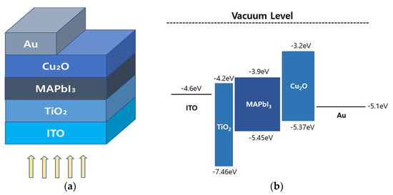
Figure 1.
(a) Basic structure of an all-inorganic multi-layer perovskite solar cell (PSC); and (b) the energy band alignment of an all-inorganic PSC.
Table 1 shows the parameters of each layer used in the simulation here. Variables not specified in Table 1 are the thermal velocity of electrons/holes of 107 cm/s, the interface defect density of 1 × 10⁻¹³ cm−3, the hole capture cross-section of the absorber/ETL of 10−18 cm2, the hole capture cross-section of the absorber/HTL of 10−19 cm2, the electron capture cross-section of the absorber/ETL of 10−19 cm2, and the electron capture cross-section of the absorber/HTL of 10−18 cm2. A series resistance of 1 Ω-cm2, shunt resistance of 4200 Ω-cm2, constant illumination of 1000 W/m2, and operating temperature of 300 K at AM 1.5G were used [55].

Table 1.
The initial physical parameters of TiO2, MAPbI3, and Cu2O used in the ITO/TiO2/MAPbI3/Cu2O/Au PSC.
3. Results and Discussion
3.1. Performance of the Perovskite Solar Cell under Initial Conditions
Prior to the optimization of each factor affecting the efficiency of PSCs, the initial conditions for the PSC device were set: an ETL TiO2 layer thickness of 100 nm, a PAL MAPbI3 layer thickness of 600 nm, and an HTL Cu2O layer thickness of 400 nm. Figure 2 shows the current density–voltage (J–V) graph of the initial PSC. The maximum optical conversion efficiency was calculated using Equations (6) and (7) [60] while considering the initial conditions as 13.79%.
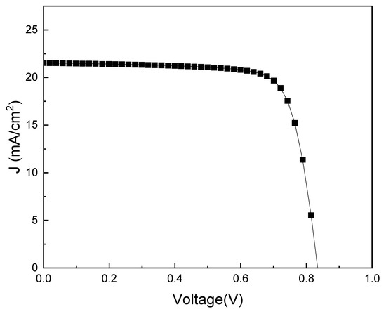
Figure 2.
Current Density-Voltage (J–V) graph for the ITO/TiO2/MAPbI3/Cu2O/Au PSC structure.
Here, FF is the fill factor, Vmax is the maximum voltage, Jmax is the maximum current density, Voc is the open-circuit voltage, Jsc is the short-circuit current density, PCE is the power conversion efficiency, and Pin is the incident power of the sun (Table 2).
Table 2.
Solar cell main parameters for the ITO/TiO₂/MAPbI3/Cu₂O/Au PSC structure.
3.2. Optimization of HTL Thickness
The PCE of PSCs is affected by the properties of ETL and HTL materials. Furthermore, the thickness of the thin film is closely related to its electrical properties, which determine the transport of electrons and holes. Thickness is also directly related to PCE. Thus, as shown in Figure 3, we first investigated the effects of thickness on the Voc, Jsc, FF, and PCE of the Cu2O HTL layer. Extremely thin HTL film forms micro-pinholes, resulting in direct contact between the absorption layer and the rear electrode, and an extremely thick HTL can increase the series resistance in the interface between the metal electrode and the HTL [61].
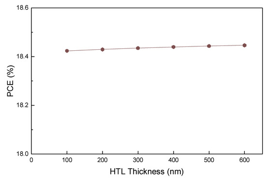
Figure 3.
PCE curve for various HTL (Cu2O) thicknesses.
Notably, as shown in Figure 3, the PCE value does not change with an increasing HTL thickness at the initial acceptor density of the HTL layer from Table 1. To understand such behavior from the PCE, the effects of HTL thickness on Voc, Jsc, and FF were examined. Similar to PCE, all these parameters remain almost constant with an increasing HTL thickness. In general, as the thickness of the charge transport layer increases, the physical distance that the charge can migrate across increases. However, the results in Figure 3 demonstrate that the PCE remains almost constant with an increasing HTL thickness. To clarify these results further, we examined the factors that had the most significant effect by changing the level of each parameter specified in Table 1. Among them, the impact of the HTL acceptor density was most significant, as shown in Figure 4, with the acceptor density of Cu2O being adjusted from 1011 to 1020 cm−3.
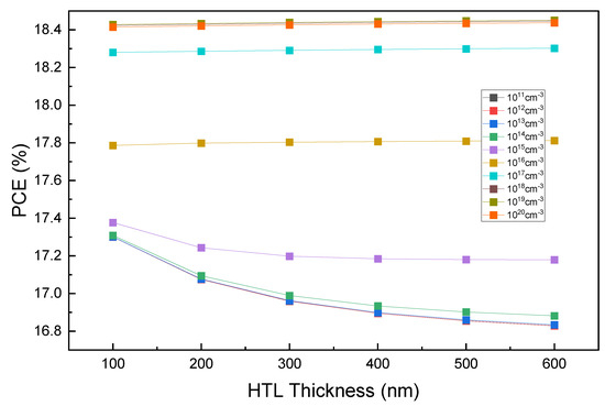
Figure 4.
HTL thickness vs. PCE curves for various HTL acceptor densities.
Figure 4 shows the PCE values according to the thickness and acceptor density of Cu2O. Figure 4 confirms that the efficiency decreases with an increasing thickness when the acceptor density of HTL is 1015 cm−3 or less. In contrast, when the acceptor density is 1016 cm−3 or higher, the PCE changes insignificantly due to the increase in thickness. To investigate the cause of this effect, the relationship between the PCE and acceptor density was examined for a 100 nm HTL thickness, where we obtained a remarkable change. Figure 5 shows the PCE as a function of the acceptor density at a Cu2O thickness of 100 nm. This result indicates that the higher the acceptor density, the greater the efficiency. In particular, the rapid increase in the values of 1016 cm−3 or higher appears to be due to the improvement of sheet resistance and conductivity at a high doping rate [62,63].
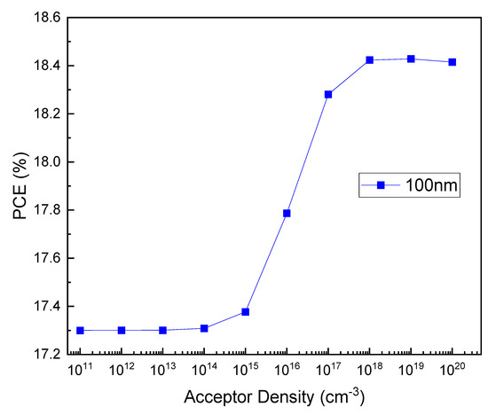
Figure 5.
Acceptor density–PCE plot for HTL thickness of 100 nm.
3.3. Optimization of Perovskite Absorber Layer Thickness
The absorption layer critically affects solar cell efficiency because it absorbs solar light and produces electron–hole pairs. Therefore, the optimization of PAL thickness is most important.
Figure 6 shows the current density–voltage (J–V) plot for various PAL thicknesses, and Figure 7 shows Voc, Jsc, FF, and PCE values as functions of PAL thickness (100–1300 nm). As shown in Figure 7d, with an increasing PAL thickness, the PCE gradually increases until the thickness of the PAL reaches 1300 nm with the highest conversion efficiency of 19.30%. Afterwards, the PCE tends to decrease with an increasing PAL thickness. This decrease in PCE was attributed to the increasing electron–hole recombination in the absorption layer, rather than the generation of electron–hole pairs [64,65,66]. The Jsc value increases as the thickness of PAL increases, which is due to improved light absorption [67]. It increases sharply from 15.18 mA/cm2 to 23.70 mA/cm2 for the range of 100–700 nm. Beyond this thickness, it increases slowly until it saturates at 24.91 mA/cm2. Additionally, as Voc increases from 100 nm to 1200 nm, PCE also increases. Afterward, from 1300 nm to 2000 nm (not shown in Figure 6), Voc slightly decreases. The initial increase in Voc indicates a reduction in charge carrier recombination within the thin absorber layer, but as the thickness increases beyond 1300 nm, the decrease in Voc could be due to a reduction in the effective bandgap and increased recombination [68].
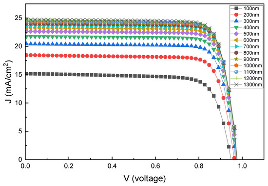
Figure 6.
Current density–voltage (J–V) curves for various PAL thicknesses.
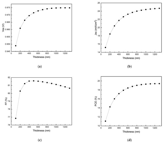
Figure 7.
Effects of PAL thickness on (a) Voc, (b) Jsc, (c) FF, and (d) PCE.
3.4. Optimization of ETL Thickness
ETL is the first layer in the PSC through which light passes, and its thickness has a significant impact on efficiency. To find out the effect of ETL on PSC, the thickness was changed from 50 to 200 nm for the simulation.
Figure 8 exhibits the current density-voltage (J–V) graphs for different ETL (TiO2) thicknesses, and Figure 9 shows the effects of ETL thickness on Voc, Jsc, FF, and PCE. As shown in Figure 9d, PCE increases with ETL thickness until the thickness of the ETL layer reaches 100 nm and decreases afterwards. The maximum PCE of 19.30% is observed at an ETL thickness of 100 nm. An overly thin ETL leads to leakage current and device failure due to discontinuity. Therefore, as the thickness increases up to 100 nm, the efficiency also increases. After reaching the maximum of 19.30% at 100 nm, the PCE efficiency decreases with an increasing ETL thickness because, similar to the HTL, the charging resistance and series resistance rapidly increase with the ETL thickness, resulting in a decrease in PCE due to absorption loss [69,70].
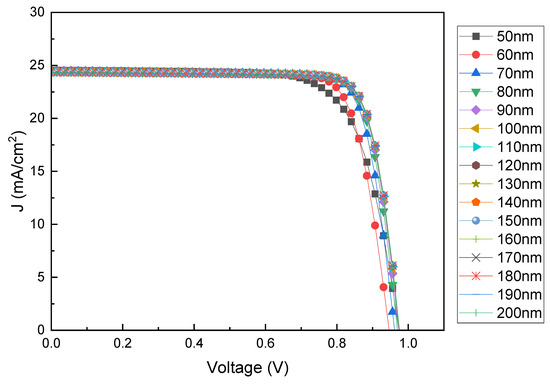
Figure 8.
Current Density-Voltage (J–V) curves for various TiO2 thicknesses.
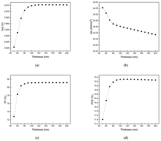
Figure 9.
Effects of ETL thickness on (a) Voc, (b) Jsc, (c) FF, and (d) PCE.
3.5. Optimization of PAL Defect Density
The defects of the absorption layer can interfere when the carriers in the device move to electrodes [71]. The PAL defect density was changed from 1010 to 1020 cm−3 to determine its effect on the PSC characteristics. Figure 10 and Figure 11 show the current density–voltage (J–V) graphs and changes in PCE according to the PAL defect densities. With an increase in defect density up to 1015 cm−3, the PCE remains at ~17%; however, with a further increase in defect density, PCE decreases to 13%. The Shockley–Read–Hall model shows that an increase in carrier life can reduce recombination [72,73,74].
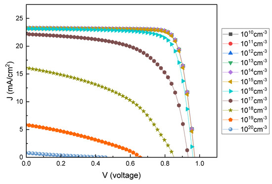
Figure 10.
The current density–voltage (J–V) curves for various PAL defect densities.
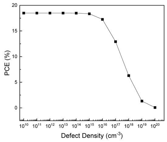
Figure 11.
Effect of PAL defect density on the PCE.
Here, τ, σ, Vth, D, and L are the minority carrier lifetime, capture cross-section, thermal velocity, diffusion coefficient, and diffusion length, respectively.
A low defect density prolongs carrier life and extends diffusion length, thereby reducing recombination (Equations (8) and (9)). Therefore, the defects in the absorption layer should be minimized to inhibit recombination.
3.6. Optimization of Interface Defect Density
The effect of the interface defect density on the PCE of PSC was investigated for the absorber/ETL and absorber/HTL interface with interface defect densities of 1013 to 1020 cm−3 (Figure 12). As shown in Figure 12a, the PCE steadily decreases as the interface defect density between the absorber and ETL layer increases. The interface defect density decreases from 18.45% to 8.26%. As shown in Figure 12b, when increasing the interface defect density of the absorber/HTL up to 1014 cm−3, the PCE also remains almost constant (18%). The PCE then decreases, reaching 17.28% at 1018 cm−3. The decrease in PCE when increasing the interface defect density was attributed to the increase in the number of traps [55].
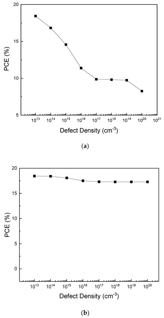
Figure 12.
PCE–defect density for (a) absorber/ETL interfaces and (b) absorber/HTL interfaces.
Comparing the range of change in Figure 12a,b, it can be seen that the change in the interface defect density between the absorber and the ETL has a greater effect on the PCE than that in the interface defect density between the absorber and the HTL. As shown in Figure 1a, upon irradiation, carriers started to be generated at the interface between absorber/ETL before those at the absorber/HTL interface. Thus, the change in the interface defect density between the absorber/ETL layer has a greater effect on the loss rate. This seems to have led to a rapid decrease in PCE [75].
3.7. Optimized PSC Device
Efficiency optimization of the ITO/TiO2/MAPbI3/Cu2O/Au structure was performed using the optimal level of each factor. Figure 13 shows the current density–voltage (J–V) graph of the optimized PSC. The initial structure is ITO/TiO2 (100 nm)/MAPbI3 (600 nm)/Cu2O (400 nm)/Au, whereas the optimized structure is ITO/TiO2 (100 nm)/MAPbI3 (1300 nm)/Cu2O (400 nm)/Au. The PCE of the optimized structure is higher by 5.51% than that of the initial structure (19.30% and 13.79%, respectively). The key factor for this increase in efficiency is considered to be the increase in PAL thickness. At a PAL thickness of 1300 nm, the PCE showed the highest value of 19.30%. The more sunlight was absorbed, the more hole–electron pairs could be created [76]. Therefore, it is thought that these increased hole–electron pairs have contributed to the enhancement of PCE.
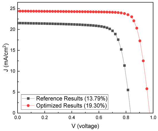
Figure 13.
Comparison of the current density–voltage (J–V) curves for the initial and optimized structures.
4. Conclusions
This study explored the influence of various parameters on the efficiency of MAPbI3 perovskite solar cells (PSCs) through SCAPS-1D simulation analysis. The examined PSC featured a layered configuration of ITO/TiO2/MAPbI3/Cu2O/Au, with a focus on the electron transport layer (ETL) thickness, perovskite absorption layer (PAL) thickness, and hole transport layer (HTL) thicknesses, as well as the PAL defect density and interface defect densities between the absorber and ETL layer and between the absorber and HTL layer. Optimal conditions achieving the highest photovoltaic conversion efficiency included an ETL (TiO2) thickness of 100 nm, PAL (MAPbI3) thickness of 1300 nm, and HTL (Cu2O) thickness of 400 nm, with a PAL defect density at 1014 cm−3 and interface defect densities at 1013 cm−3 for both the absorber/ETL interfaces and absorber/HTL interfaces. These optimizations enhanced the PSC’s power conversion efficiency (PCE) to 19.30%, a significant increase from the baseline of 13.79% by 5.51%. The findings of this study are expected to contribute significantly to the optimization and efficiency enhancement of perovskite solar cells, particularly those employing inorganic charge carrier transport layers.
Author Contributions
Conceptualization, C.S. and B.-S.J.; software, C.S. and H.S.; methodology, C.S. and B.-S.J.; formal analysis, C.S., H.S. and B.-S.J.; writing—original draft preparation, C.S.; writing—review and editing, B.-S.J.; supervision, B.-S.J. All authors have read and agreed to the published version of the manuscript.
Funding
This work was supported by KNU Advanced Material Research Institute, Kyungpook National University, Daegu 41566, Republic of Korea.
Institutional Review Board Statement
Not applicable.
Informed Consent Statement
Not applicable.
Data Availability Statement
The data presented in this study are available upon request from the corresponding author.
Conflicts of Interest
The authors declare no conflict of interest.
References
- Rong, Y.; Hu, Y.; Mei, A.; Tan, H.; Saidaminov, M.; Seok, S.; Mcgehee, M.; Sargent, E.; Han, H. Challenges for commercializing perovskite solar cells. Science 2018, 361, eaat8235. [Google Scholar] [CrossRef]
- Qian, J.; Xu, B.; Tian, W. A comprehensive theoretical study of halide perovskites ABX3. Org. Electron. 2016, 37, 61–73. [Google Scholar] [CrossRef]
- Hsiao, K.; Ho, C.; Lin, T.; Chen, S.; Chang, Y.; Liao, Y.; Chang, J.; Lin, T.; Huang, Y.; Lee, K.; et al. Ceiling of Barium substitution for B-Site cation in organometal halide perovskite solar Cells. Int. J. Energy Res. 2024, 2024, 990559. [Google Scholar] [CrossRef]
- Kojima, A.; Teshima, K.; Shirai, Y.; Miyasaka, T. Organometal halide perovskites as visible-light sensitizers for photovoltaic cells. J. Ameri. Chem. Soc. 2009, 131, 6050–6051. [Google Scholar] [CrossRef] [PubMed]
- National Renewable Energy Labs (NREL). Best Research-Cell Efficiency Chart. Available online: https://www.nrel.gov/pv/assets/pdfs/cell-pv-eff-emergingpv-rev220630.pdf (accessed on 12 February 2023).
- Kumar, N.; Rani, J.; Kurchania, R. A review on power conversion efficiency of lead iodide perovskite-based solar cells. Mater. Today Proc. 2021, 46, 5570–5574. [Google Scholar] [CrossRef]
- Chiu, Y.; Chen, S.; Lee, K.; Lin, T.; Wu, M. Side chain modulated carbazole-based bifunctional hole-shuttle interlayer simultaneously improves interfacial energy level alignment and defect passivation in high-efficiency perovskite solar cells. Chem. Eng. J. 2023, 477, 147208. [Google Scholar] [CrossRef]
- Jeong, J.; Kim, M.; Seo, J.; Lu, H.; Ahlawat, P.; Mishra, A.; Kim, J.Y. Pseudo-halide anion engineering for α-FAPbI3 perovskite solar cells. Nature 2021, 592, 381–385. [Google Scholar] [CrossRef]
- Nazeeruddin, M.; Snaith, H. Methylammonium lead triiodide perovskite solar cells: A new paradigm in photovoltaics. MRS Bull. 2015, 40, 641–645. [Google Scholar] [CrossRef]
- Sun, P.; Li, Q.; Yang, L.; Li, Z. Theoretical insights into a potential lead-free hybrid perovskite: Substituting Pb 2+ with Ge 2+. Nanoscale 2016, 8, 1503–1512. [Google Scholar] [CrossRef]
- Smecca, E.; Numata, Y.; Deretzis, I.; Pellegrino, G.; Boninelli, S.; Miyasaka, T.; La Magna, A.; Alberti, A. stability of solution-processed MAPbI3 and FAPbI3 Layers. Phys. Chem. Chem. Phys. 2016, 18, 13413–13422. [Google Scholar] [CrossRef]
- Yang, J.; Kelly, T. Decomposition and Cell Failure Mechanisms in Lead Halide Perovskite Solar Cells. Inorg. Chem. 2017, 56, 92–101. [Google Scholar] [CrossRef]
- Liang, J.; Wang, C.; Wang, Y.; Xu, Z.; Lu, Z.; Ma, Y.; Zhu, H.; Hu, Y.; Xiao, C.; Yi, X. All-Inorganic Perovskite Solar Cells. J. Am. Chem. Soc. 2016, 138, 15829–15832. [Google Scholar] [CrossRef]
- Yuan, H.; Zhao, Y.; Duan, J.; Wang, Y.; Yang, X.; Tang, Q. All-Inorganic CsPbBr3 perovskite solar cell with 10.26% efficiency by spectra engineering. J. Mater. Chem. A 2018, 6, 24324–24329. [Google Scholar] [CrossRef]
- Petti, L.; Münzenrieder, N.; Vogt, C.; Faber, H.; Büthe, L.; Cantarella, G.; Bottacchi, F.; Anthopoulos, T.; Tröster, G. Metal Oxide Semiconductor Thin-Film Transistors for Flexible Electronics. Appl. Phys. Rev. 2016, 3, 021303. [Google Scholar] [CrossRef]
- Uwihoreye, V.; Yang, Z.; Zhang, J.; Lin, Y.; Liang, X.; Yang, L.; Zhang, K. Transparent conductive SnO2 thin films via resonant Ta doping. Sci. China Mater. 2022, 66, 264–271. [Google Scholar] [CrossRef]
- Wang, Q.; Hu, J.; Song, A. Influence of Oxygen Flow on Structural, Optical, and Electrical Properties of Al:SnO2 Films Deposited at Room Temperature. J. Electron. Mater. 2024, 53, 2094–2103. [Google Scholar] [CrossRef]
- Boucherka, T.; Touati, M.; Berbadj, A.; Brihi, N. Al3+ doping induced changes of structural, morphology, photoluminescence, optical and electrical properties of SnO2 thin films as alternative TCO for optoelectronic applications. Ceram. Int. 2023, 49, 5728–5737. [Google Scholar] [CrossRef]
- Laghrib, S.; Benhaliliba, M.; Adnani, H.; Abdi, D. Wide bandgap Indium-doped SnO2 semiconductor prepared by solgel route: Multilayer fabrication and Low resistivity for solar cell application. J. Sol-Gel Sci. Technol. 2023, 106, 530–544. [Google Scholar] [CrossRef]
- Senthilkumar, P.; Raja, S.; Babu, R.; Kavinkumar, V.; Jothivenkatachalam, K.; Vasuki, G. Impact of Ta doping on the optoelectronic and catalytic properties of SnO2 thin films. Appl. Phys. A 2023, 129, 675. [Google Scholar] [CrossRef]
- Craciun, V.; Elders, J.; Gardeniers, J.; Boyd, I.W. Characteristics of High Quality ZnO Thin Films Deposited by Pulsed Laser Deposition. Appl. Phys. Lett. 1994, 65, 2963–2965. [Google Scholar] [CrossRef]
- Prasad, S.; Bansal, S.; Mansoori, A.; Bala, M.; Sharma, P. Effect of Annealing Temperature on Excitonic Binding Energy and Other Optical Properties of Mn-Ni Co-Doped Transparent ZnO Thin Films. Trans. Ind. Ceram. Soc. 2023, 82, 31–39. [Google Scholar] [CrossRef]
- Zagal-Padilla, C.; Gamboa, S. Role of native defects on the opto-electronic properties of p-type ZnO synthesized during the most straightforward method: Only water. Appl. Phys. A 2023, 129, 183. [Google Scholar] [CrossRef]
- Zhao, Y.; Ding, W.; Xiao, Y.; Yang, P. First-principles study on p-type transformation of ZnO doped by Ag element. Phys. B 2023, 657, 414810. [Google Scholar] [CrossRef]
- Yang, R.; Wang, F.; Lu, J.; Lu, Y.; Lu, B.; Li, S.; Ye, Z. ZnO with p-Type Doping: Recent Approaches and Applications. ACS Appl. Electron. Mater. 2023, 5, 4014–4034. [Google Scholar] [CrossRef]
- Shin, H.; Choi, S.; Hong, S.; Lee, C.; Oh, D.; Bae, S.; Kim, T.; Song, H.; Kim, H.; Oh, C. Technical Progress of OLED Displays for Premium TVs. SID Dig. 2022, 53, 673–676. [Google Scholar] [CrossRef]
- Shin, H.; Kim, Y.; Kim, D.; Yun, S.; Bae, S.; Kim, H.; Lee, H.; Oh, C. A novel ultra large size organic light emitting diode display for premium televisions. J. Soc. Inf. Display 2023, 31, 253–263. [Google Scholar] [CrossRef]
- Aslam, M.; Abdullah, A.; Rafatullah, M. Recent development in the green synthesis of titanium dioxide nanoparticles using plant-based biomolecules for environmental and antimicrobial applications. J. Ind. Eng. Chem. 2021, 98, 1–16. [Google Scholar] [CrossRef]
- Medhi, R.; Marquez, M.; Lee, T. Visible-light-active doped metal oxide nanoparticles: Review of their synthesis, properties, and applications. ACS Appl. Nano Mater. 2020, 3, 6156–6185. [Google Scholar] [CrossRef]
- Rajendran, S.; Karimi-Maleh, H.; Qin, J.; Lichtfouse, E. Metal, Metal-Oxides and Metal Sulfides for Batteries, Fuel Cells, Solar Cells, Photocatalysis and Health Sensors; Springer: Cham, Switzerland, 2021; pp. 147–168. [Google Scholar]
- Chen, J.; Park, N. Inorganic Hole Transporting Materials for Stable and High Efficiency Perovskite Solar Cells. J. Phys. Chem. C 2018, 122, 14039–14063. [Google Scholar] [CrossRef]
- Hossain, M.; Hasan, A.; Qarony, W.; Shahiduzzaman, M.; Islam, M.; Ishikawa, Y.; Uraoka, Y.; Amin, N.; Knipp, D.; Akhtaruzzaman, M. Electrical and Optical Properties of Nickel-Oxide Films for Efficient Perovskite Solar Cells. Small Methods 2020, 4, 2000454. [Google Scholar] [CrossRef]
- Kung, P.; Li, M.; Lin, P.; Chiang, Y.; Chan, C.; Guo, T.; Chen, P. A Review of Inorganic Hole Transport Materials for Perovskite Solar Cells. Adv. Mater. Interfaces. 2018, 5, 1800882. [Google Scholar] [CrossRef]
- Pavoni, E.; Modreanu, M.; Mohebbi, E.; Mencarelli, D.; Stipa, P.; Laudadio, E.; Pierantoni, L. First-Principles Calculation of MoO2 and MoO3 Electronic and Optical Properties Compared with Experimental Data. Nanomaterials 2023, 13, 1319. [Google Scholar] [CrossRef]
- Lee, H. Thickness Dependence of MoO3 Hole Injection Layer on Energy-Level Alignment with NPB Hole Transport Layers in OLEDs. Appl. Sci. Converg. Technol. 2023, 32, 73–76. [Google Scholar] [CrossRef]
- Bericat-Vadell, R.; Zou, X.; Drillet, M.; Corvoysier, H.; Silveira, V.; Konezny, S.; Sá, J. Carrier Dynamics in Solution-Processed CuI as a P-Type Semiconductor: The Origin of Negative Photoconductivity. J. Phys. Chem. Lett. 2023, 14, 1007–1013. [Google Scholar] [CrossRef] [PubMed]
- Woods-Robinson, R.; Han, Y.; Zhang, H.; Ablekim, T.; Khan, I.; Persson, K.; Zakutayev, A. Wide Band Gap Chalcogenide Semiconductors. Chem. Rev. 2020, 120, 4007–4055. [Google Scholar] [CrossRef] [PubMed]
- Willis, J.; Claes, R.; Zhou, Q.; Giantomassi, M.; Rignanese, G.; Hautier, G.; Scanlon, D. Limits to Hole Mobility and Doping in Copper Iodide. Chem. Mater. 2023, 35, 8995–9006. [Google Scholar] [CrossRef]
- Liu, A.; Zhu, H.; Park, W.; Kim, S.; Kim, H.; Kim, M.; Noh, Y. High-performance p-channel transistors with transparent Zn doped-CuI. Nat. Commun. 2020, 11, 4309. [Google Scholar] [CrossRef]
- Nandi, P.; Park, H.; Shin, S.; Lee, J.; Kim, J.; Ko, M.; Jung, H.; Park, N.; Shin, H. NiO as Hole Transporting Layer for Inverted Perovskite Solar Cells: A Study of X-Ray Photoelectron Spectroscopy. Adv. Mater. Interfaces 2023, 2300751. [Google Scholar] [CrossRef]
- Njema, G.; Kibet, J. A Review of the Technological Advances in the Design of Highly Efficient Perovskite Solar Cells. Int. J. Photoenergy 2023, 2023, 3801813. [Google Scholar] [CrossRef]
- Grandhi, K.; Hardy, D.; Krishnaiah, M.; Vargas, B.; Al-Anesi, B.; Suryawanshi, M.; Solis-Ibarra, D.; Gao, F.; Hoye, R.; Vivo, P. Wide-Bandgap Perovskite-Inspired Materials: Defect-Driven Challenges for High-Performance Optoelectronics. Adv. Funct. Mater. 2023, 2307441. [Google Scholar] [CrossRef]
- Qin, J.; Che, Z.; Kang, Y.; Liu, C.; Wu, D.; Yang, H.; Hu, X.; Zhan, Y. Towards operation-stabilizing perovskite solar cells: Fundamental materials, device designs, and commercial applications. InfoMat 2024, e12522. [Google Scholar] [CrossRef]
- Huang, P.; Chen, S.; Chao, L.; Xie, J.; Liao, C.; Tseng, Z.; Chen, S. Efficient CsPbBr3 Quantum-Dot Light-Emitting Diodes Using Sputtered NiO Films as Hole Injection Layers. Materials 2023, 16, 6060. [Google Scholar] [CrossRef] [PubMed]
- Lin, J.; Dai, X.; Liang, X.; Chen, D.; Zheng, X.; Li, Y.; Deng, Y.; Du, H.; Ye, Y.; Chen, D.; et al. High-Performance Quantum-Dot Light-Emitting Diodes Using NiOx Hole-Injection Layers with a High and Stable Work Function. Adv. Funct. Mater. 2020, 30, 1907265. [Google Scholar] [CrossRef]
- Gao, F.; Liu, X.; Zhang, J.; Song, M.; Li, N. Photovoltaic properties of the p-CuO/n-Si heterojunction prepared through reactive magnetron sputtering. J. Appl. Phys. 2012, 111, 084507. [Google Scholar] [CrossRef]
- Kuo, C.; Huang, M. Morphologically controlled synthesis of Cu2O nanocrystals and their properties. Nano Today 2010, 5, 106–116. [Google Scholar] [CrossRef]
- Sun, S.; Yang, Z. Recent advances in tuning crystal facets of polyhedral cuprous oxide architectures. RSC Adv. 2014, 4, 3804–3822. [Google Scholar] [CrossRef]
- Sun, S. Recent advances in hybrid Cu2O-based heterogeneous nanostructures. Nanoscale 2015, 7, 10850–10882. [Google Scholar] [CrossRef]
- Burgelman, M.; Verschraegen, J.; Degrave, S.; Nollet, P. Modeling thin-film PV devices. Prog. Photovolt. Res. Appl. 2004, 12, 143–153. [Google Scholar] [CrossRef]
- Burgelman, M.; Nollet, P.; Degrave, S. Modelling polycrystalline semiconductor solar cells. Thin Solid Films 2000, 361, 527–532. [Google Scholar] [CrossRef]
- Mostefaoui, M.; Mazari, H.; Khelifi, S.; Bouraiou, A.; Dabou, R. Simulation of high efficiency CIGS solar cells with SCAPS-1D software. Energy Procedia 2015, 74, 736–744. [Google Scholar] [CrossRef]
- Rasool, R.; Mohammed, A.A.; Hasan, R.F. Study Effects of Illumination and Temperature on Performance of (pn-Si) Device using Simulation Program SCAPS-1D. Iraqi J. Sci. 2021, 62, 1524–1536. [Google Scholar] [CrossRef]
- Movla, H. Optimization of the CIGS based thin film solar cells: Numerical simulation and analysis. Optik 2014, 125, 67–70. [Google Scholar] [CrossRef]
- Ahmed, S.; Jannat, F.; Khan, M.A.K.; Alim, M.A. Numerical development of eco-friendly Cs2TiBr6 based perovskite solar cell with all-inorganic charge transport materials via SCAPS-1D. Optik 2021, 225, 165765. [Google Scholar] [CrossRef]
- Stanić, D.; Kojić, V.; Čižmar, T.; Juraić, K.; Bagladi, L.; Mangalam, J.; Gajović, A. Simulating the performance of a formamidinium based mixed cation lead halide perovskite solar cell. Materials 2021, 14, 6341. [Google Scholar] [CrossRef] [PubMed]
- Khattak, Y.; Baig, F.; Shuja, A.; Beg, S.; Soucase, B. Numerical analysis guidelines for the design of efficient novel nip structures for perovskite solar cell. Sol. Energy 2020, 207, 579–591. [Google Scholar] [CrossRef]
- Bhavsar, K.; Lapsiwala, P. Numerical simulation of perovskite solar cell with different material as electron transport layer using SCAPS-1D software. Semicond. Phys. Quantum Electron. Optoelectron. 2021, 24, 341–347. [Google Scholar] [CrossRef]
- Sawicka-Chudy, P.; Starowicz, Z.; Wisz, G.; Yavorskyi, R.; Zapukhlyak, Z.; Bester, M.; Głowa, Ł.; Sibiński, M.; Cholewa, M. Simulation of TiO2/CuO Solar Cells with SCAPS-1D Software. Mater. Res. Express 2019, 6, 085918. [Google Scholar] [CrossRef]
- Kitai, A. Principles of Solar Cells, LEDs and Diodes: The Role of the PN Junction; John Wiley & Sons: Chichester, UK, 2011; pp. 160–184. [Google Scholar]
- Jannat, F.; Ahmed, S.; Alim, M. Performance analysis of cesium formamidinium lead mixed halide based perovskite solar cell with MoOx as hole transport material via SCAPS-1D. Optik 2021, 228, 166202. [Google Scholar] [CrossRef]
- Kothandapani, Z.; Islam, M.A.; Reza, Y.; Hasana, A.A.; Amin, N. Optimization of Cu2O and CuSCN as htl of planar perovskite solar cells via numerical simulation. J. Ovonic Res. 2020, 16, 369–377. [Google Scholar] [CrossRef]
- Agha, D.; Algwari, Q. The influence of the interface layer between the electron transport layer and absorber on the performance of perovskite solar cells. IOP Conf. Ser. Mater. Sci. Eng. 2021, 1152, 012033. [Google Scholar] [CrossRef]
- Devi, C.; Mehra, R. Device simulation of lead-free MASnI3 solar cell with CuSbS2 (copper antimony sulfide). J. Mater. Sci. 2019, 54, 5615–5624. [Google Scholar] [CrossRef]
- Bag, A.; Radhakrishnan, R.; Nekovei, R.; Jeyakumar, R. Effect of absorber layer, hole transport layer thicknesses, and its doping density on the performance of perovskite solar cells by device simulation. Sol. Energy 2020, 196, 177–182. [Google Scholar] [CrossRef]
- Koishiyev, G.; Sites, J. Impact of sheet resistance on 2-D modeling of thin-film solar cells. Sol. Energy. Mater. Sol. Cells 2009, 93, 350–354. [Google Scholar] [CrossRef]
- Xing, G.; Mathews, N.; Sun, S.; Lim, S.; Lam, Y.; Grätzel, M.; Sum, T. Long-range balanced electron-and hole-transport lengths in organic-inorganic CH3NH3PbI3. Science 2013, 342, 344–347. [Google Scholar] [CrossRef] [PubMed]
- Pazos-Outón, L.; Xiao, T.; Yablonovitch, E. Fundamental efficiency limit of lead iodide perovskite solar cells. J. Phys. Chem. Lett. 2018, 9, 1703–1711. [Google Scholar] [CrossRef] [PubMed]
- Sun, W.; Choy, K.; Wang, M. The role of thickness control and interface modification in assembling efficient planar perovskite solar cells. Molecules 2019, 24, 3466. [Google Scholar] [CrossRef]
- Jeyakumar, R.; Bag, A.; Nekovei, R.; Radhakrishnan, R. Influence of electron transport layer (TiO2) thickness and its doping density on the performance of CH3NH3PbI3-based planar perovskite solar cells. J. Electron. Mater. 2020, 49, 3533–3539. [Google Scholar] [CrossRef]
- Abdelaziz, S.; Zekry, A.; Shaker, A.; Abouelatta, M. Investigating the performance of formamidinium tin-based perovskite solar cell by SCAPS device simulation. Opt. Mater. 2020, 101, 109738. [Google Scholar] [CrossRef]
- Du, H.; Wang, W.; Zhu, J. Device simulation of lead-free CH3NH3SnI3 perovskite solar cells with high efficiency. Chin. Phys. B 2016, 25, 108802. [Google Scholar] [CrossRef]
- Zekry, Z.; Eldallal, G. Effect of MS contact on the electrical behaviour of solar cells. Solid-State Electron. 1988, 31, 91–97. [Google Scholar] [CrossRef]
- Cheng, H.; Feng, Y.; Fu, Y.; Zheng, Y.; Shao, Y.; Bai, Y. Understanding and minimizing non-radiative recombination losses in perovskite light-emitting diodes. J. Mater. Chem. C 2022, 10, 13590–13610. [Google Scholar] [CrossRef]
- Lin, L.; Jiang, L.; Li, P.; Fan, B.; Qiu, Y. A modeled perovskite solar cell structure with a Cu2O hole-transporting layer enabling over 20% efficiency by low-cost low-temperature processing. J. Phys. Chem. Solids 2019, 124, 205–211. [Google Scholar] [CrossRef]
- Khoshsirat, N.; Yunus, N.; Hamidon, M.; Shafie, S.; Amin, N. Analysis of absorber layer properties effect on CIGS solar Cell performance using SCAPS. Optik 2015, 126, 681–686. [Google Scholar] [CrossRef]
Disclaimer/Publisher’s Note: The statements, opinions and data contained in all publications are solely those of the individual author(s) and contributor(s) and not of MDPI and/or the editor(s). MDPI and/or the editor(s) disclaim responsibility for any injury to people or property resulting from any ideas, methods, instructions or products referred to in the content. |
© 2024 by the authors. Licensee MDPI, Basel, Switzerland. This article is an open access article distributed under the terms and conditions of the Creative Commons Attribution (CC BY) license (https://creativecommons.org/licenses/by/4.0/).