Article

Research on a Partial Discharge Expert System for the Diagnosis of Damaged Transformation Equipment

1
Department of Electrical Engineering, National Taiwan University of Science and Technology, Taipei 10607, Taiwan
2
National Atomic Research Institute, Taoyuan City 32546, Taiwan
*
Author to whom correspondence should be addressed.
Appl. Sci. 2024, 14(3), 1195; https://doi.org/10.3390/app14031195
Submission received: 18 December 2023 / Revised: 23 January 2024 / Accepted: 26 January 2024 / Published: 31 January 2024

Abstract

:
Partial discharge (PD) characteristics are very important for the diagnosis of damaged transformation equipment. If the power transmission and transformation equipment fails, it will cause large economic losses, and thus prevention is better than treatment. One of the effective methods for high-voltage insulation degradation detection is to observe the phenomenon of partial discharge of equipment, which is the earliest characteristic. Prevention can be carried out in advance, and trend observation is better than periodic inspection. Long-term observation can effectively reduce the probability of misjudgment. This project intends to develop a high-speed data-acquisition device to acquire the original discharge waveform data of partial discharge for noise suppression. In order to improve the diagnostic efficiency and accuracy of the diagnostic system, it is necessary to suppress the noise of the measurement data, so as to carry out the fault identification of the discharge type. Through this method, the actual operating data of the system can be recorded as the original discharge waveform, in order to understand the original discharge waveform conditions of the power transmission and transformation equipment in multiple partial discharge measurements, and then after noise suppression, it can be regarded as a type of partial discharge identification.

1. Introduction

The majority of damages to substation transmission and transformation equipment are due to insulation degradation, which is usually an aging phenomenon caused by electrical stress, thermal stress, or mechanical stress. These aging phenomena are further accelerated by partial discharge (PD), leading to serious accidents. To prevent major accidents, it is essential to have real-time knowledge of the equipment’s condition. In the operation of the power system, the high-voltage power equipment is responsible for the supply, transmission, and distribution of electricity [1,2,3,4]. Given the increasing complexity of the power system and the demand for power going up, insulation defects of high-voltage power equipment will cause serious power outages, equipment damage, economic loss, and inconvenience to the industry, and even equipment failure and human casualties. To prevent such incidents from happening, the prediction and preventive measurement of insulation defects have become the main subject of research. PD measurement has been identified as a reliable insulation evaluation diagnostic tool for high-voltage equipment, as voids, cracks, and gaps are significant defects in dielectric materials, whether in solid, liquid, or gas form. When electrical equipment is subjected to high-pressure stress that will cause physical and chemical degradation of the insulation interface, PD measurement is significant for the characterization of its insulation state [5,6]. PD measurement methods include pulse current, ultrasonic, and ultra-high frequency methods [7,8]. Although numerous studies have used the amount of PD charge integrated from the PD pulse current, few studies have measured the high-speed nanosecond PD pulse current itself, which is easily buried in noise [9]. To satisfy the requirements, one may use a high-speed A/D-acquisition card or oscilloscope [10]. For example, a high-speed data acquisition unit is used to obtain complete discharge waveform information in a power frequency cycle. PD in this study is a tiny signal that occurs due to an insulation defect of the power supply equipment that is usually accompanied by physical phenomena such as light, sound, and heat; we aimed to develop a self-made portable partial discharge analyzer for its detection. PD inspection is an effective technology to evaluate the condition of the insulation components of power equipment. It can replace defective insulation components in advance to ensure a stable power supply [11,12,13]. Under the influence of a strong electric field, some of the defects in the internal insulation of the equipment, such as bubble gaps, impurities, and spikes or points all cause uneven electric field distribution inside the equipment insulation [14]. The PD, which is the electric field intensity of the defective component, increases, which can easily cause discharge and does not penetrate the overall insulation [15]. On the other hand, PD inside the insulation of high-voltage electrical equipment will affect the service life of the insulation. These PD phenomena include needle plate discharge, creeping discharge, air-gap discharge, and metal-particle discharge [16]. PD occurs in degraded high-voltage insulation. The specification of IEC60270 defines partial discharge as only the partially bridging the insulation between conductors and states that it may or may not happen near the conductor. PD is usually the result of a local electric stress concentration in or on the surface of an insulator. Usually, this discharge is a pulse lasting much less than one microsecond. These discharges will cause the resistance to decrease and ultimately lead to malfunction. Each discharge represents a current pulse. The monitoring of these pulses is a mature technology for evaluating the insulation status of high-voltage equipment [17]. Traditional techniques for detecting PD current pulses include high-frequency current sensors (HFCT), transient ground voltage sensors (TEV), and UHF sensors [18]. The classification of PD modes is the basic criterion for evaluating and diagnosing the performance of insulation systems, because it provides a significant indicator of the severity of the discharge. In order to evaluate the insulation status of the equipment, this uniqueness must be used to correlate the discharge pattern with the defect type. PD diagnosis is completed by visual inspection in the initial stage. Due to the difficulty of detecting PD, only experts with rich personal experience can distinguish various discharge phenomena and evaluate the severity of the fault [19].

2. Materials and Methods

2.1. Hardware Architecture

The hardware architecture of the homemade partial discharge analyzer, as shown in Figure 1, is divided into two main components: the data-acquisition module and the embedded system.
We designed and improved the data-acquisition module based on the literature [20]. As Figure 2 shows, there are six analog synchronization input channels, the resolution of each channel is 12 bits, and the maximum sampling rate is up to 65 MS/s, with 256 MB DDR3 memory; each piece of data is calculated by using bits, and up to 67,108,864 datapoints can be stored. The adjustable input voltage range is: ±5 V, ±2 V, ±1 V, ±0.5 V. Design with FPGA includes a communication controller, memory controller, ADC controller, and frequency controller. We changed the transmission mode from an asynchronous nonmultiplexed device to a synchronous address/data-multiplexed device to increase the transmission speed. Asynchronous and synchronous devices have different ways of judging. The asynchronous device uses a WE or OE signal to judge. The synchronous device uses GPMC_CLK to judge. In the synchronous model, the address is only sent once before starting the transfer, and subsequently it is automatically increased by 1 each time according to the CLK, and thus address line errors can be avoided. The difference is whether the transmission position is continuous, and it is the continuous position in this case. Therefore, a synchronous address/data-multiplexed device is more suitable. At the same time, the address/data-multiplexed address line and data line can be multiplexed, and the hardware circuit is omitted.
In the literature [2], the FPGA parallel-port design uses a GPMC with the asynchronous 16-bit address/data-non-multiplexed method without a DMA to transmit data with an ARM. The data line and the address line are independent, so there is no need for a CLK or a CS trigger to transmit data. A CS trigger can send 8 bytes in around 500 ns, which is equivalent to the transmission speed of 128 Mbps. As shown in the transmission interface synchronous 16-bit address/data-multiplexed GPMC with DMA in this study, the DMA can increase transmission continuity, and there is no need to switch jobs due to the multi-threading of the ARM system to achieve the increase in the transmission speed. In this transmission mode, the address is transmitted first, and then the address must be incremented—in burst mode, up to 32 bytes of data can be transmitted each time, the transmission time is 400 ns, and the transmission speed is equivalent to 640 Mbps. In actual transmission, it takes some time, due to the Linux execution program, system thread conversion, hardware settings, etc. The original transmission time is about 30 s and is reduced to less than 5 s to achieve the purpose of increasing the transmission speed.

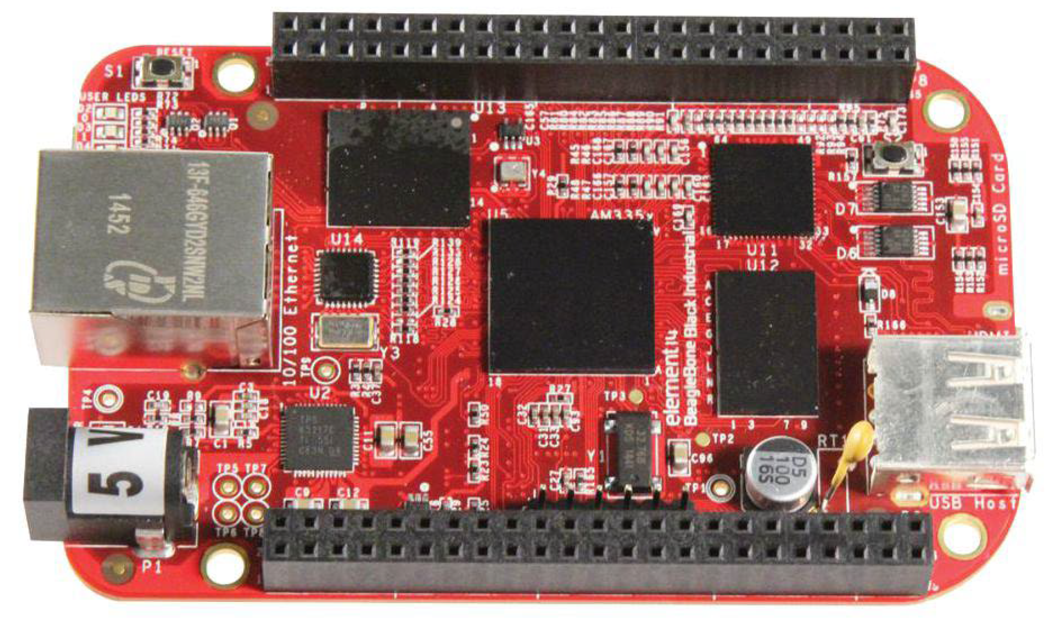
2.1.1. Embedded ARM Processor

The PD raw discharge waveform acquisition system in this study utilizes the Texas Instruments TI Sitara Processor AM3358 processor, which is based on the ARM Cortex-A8 architecture. The processor specifications and development board are depicted in Figure 2.

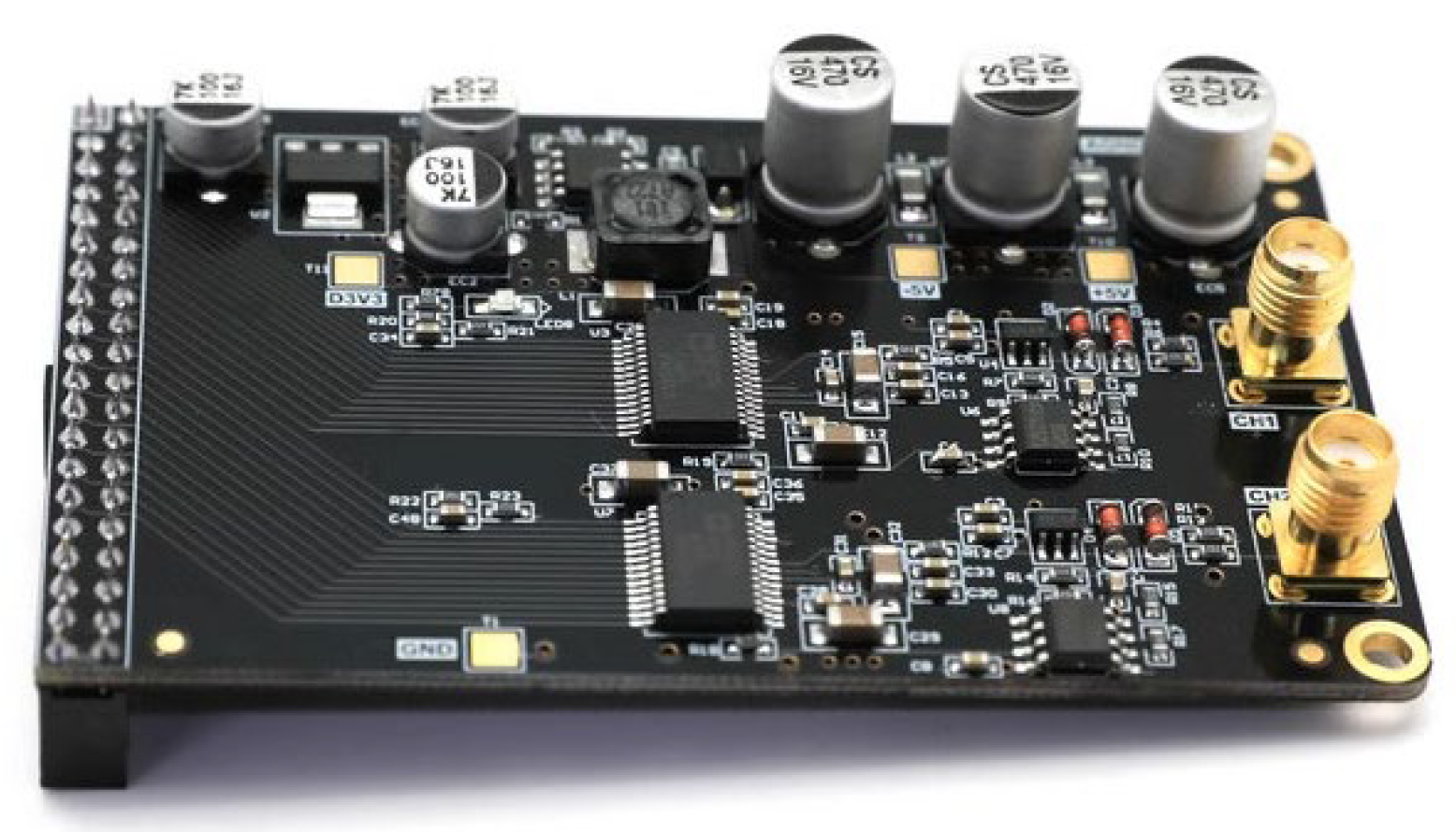
2.1.2. Analog-to-Digital Converter

The local raw discharge waveform measurement system employs the Analog Devices Inc. (ADI) AD9226 high-speed analog-to-digital converter (ADC) due to the approximate 10 MHz frequency of the raw discharge waveform. The AD9226 analog-to-digital conversion module is depicted in Figure 3. The AD9226 operates with a single power supply and features a high-performance amplifier and reference voltage source, offering a voltage resolution of up to 12 bits and a sampling rate of up to 65 MS/s. It can be applied in various applications such as ultrasound, imaging, and communication systems, making it suitable for multi-channel multiplexing systems for detecting voltage ranges in high-frequency continuous signals. It can also perform single-channel sampling at the Nyquist rate and has a rated temperature range of −40 °C to +85 °C.

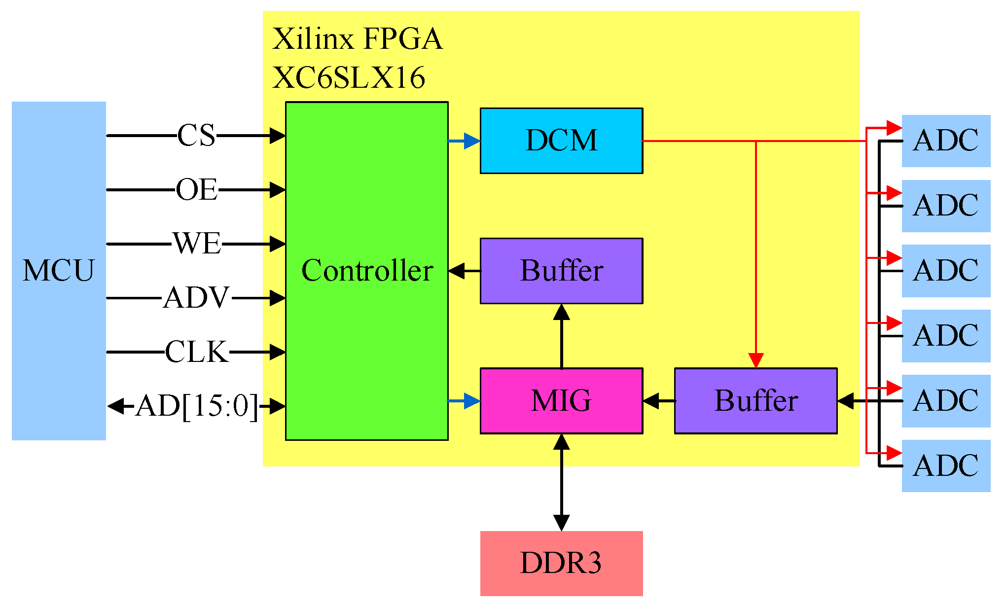
2.1.3. Field Programmable Gate Array

The on-site field programmable gate array (FPGA) utilizes the Xilinx Spartan-6, which allows for programmable routing using logic blocks, creating custom hardware functions from configured chips. FPGA possesses the property of reconfigurability and can be modified according to specific usage requirements.
FPGA integrates application-specific integrated circuit (ASIC) and processor architecture systems, offering hardware clock speed and reliability, reducing the cost of custom ASIC design, and allowing for chip reprogramming in a manner similar to software flexibility. It is not limited by the number of processor cores. Additionally, FPGA is a parallel architecture, so different processing tasks do not occupy the same resources. Each independent processing task is assigned to a dedicated chip block, which does not affect other logic blocks and can automatically generate functions. Therefore, when adding other processing tasks, the performance of the application section is not affected.
FPGA is a powerful and flexible hardware platform, as shown in Figure 4, and is particularly suitable for scenarios that require high customization and high-performance computing. However, due to its relatively complex development process, it typically requires specialized hardware design and electronic engineering knowledge.

2.1.4. Technical Architecture of High-Speed Data-Acquisition Device System

The analog-to-digital converter (ADC) in the system used for capturing the raw discharge waveform of PD employs an FPGA as the controller for the ADC to achieve a higher sampling rate, meeting the requirements for transmission speed.
The FPGA circuit functions designed in this study, as depicted in Figure 5, include a controller. The design adopts a parallel approach to allow data transmission between the microcontroller unit (MCU) and the controller. The parallel port connection lines include chip select (CS), output enable (OE), write enable (WE), address valid (ADV), clock (CLK), and address data (AD) lines. Additionally, there is a digital clock manager (DCM) used for configuring and controlling the sampling rate of the analog-to-digital converter, as well as a memory interface generator (MIG) for controlling the write and read operations of the DDR3 memory. Finally, if there are differences in the data width or transmission rates during data transmission, a buffer must be added in the middle of the transmission.

2.2. Functions and Processes of System Software and Data Acquisition Systems

The high-speed data-acquisition software system functions of the raw discharge waveform-detection system for PD utilize ARM processor design and development. The high-speed data-acquisition software system functions encompass FPGA driver programs, ADC sampling and acquisition control programs, and data transmission interfaces.
The process control requires loading the driver program for FPGA communication into the system core. In Linux, a driver is a special kernel module used for communication with hardware devices. Through the driver, the operating system and applications can interact with hardware devices. Kernel modules are pieces of code that can be dynamically loaded and unloaded at runtime. These modules essentially act as plugins that extend the functionality of the Linux kernel, allowing developers to add new features or update existing ones without altering the entire kernel source code or recompiling the kernel.
Setting the ADC sampling rate length and threshold values can be configured through the REST API, allowing for the initiation of analog data acquisition. After the conversion is completed, the high-speed data acquisition of the local discharge raw waveform can be transmitted to the embedded system via transmission commands. Finally, the data of the local discharge raw waveform can be obtained through the REST API.

2.2.1. Software System User Interface Design

The graphical user interface (GUI) of the raw discharge waveform-detection system for PD is designed to interface with Jupyter, as shown in Figure 6. Jupyter is an interactive environment used for data analysis, machine learning, statistical modeling, and other mathematical computations. The most common form is Jupyter Notebook, which is a web application that can contain code, documents, mathematical formulas, and visualization tools.
The high-speed data-acquisition device used for local discharge raw waveform detection employs a communication technology framework based on REST API (representational state transfer application programming interface). REST API is a software architectural style used for developing web services. It enables the exchange of data between clients and servers over the HTTP protocol. REST API is typically used to build and provide resource-oriented services, and it models resources or data entities using URIs (uniform resource identifiers).
The human–machine interface design of the high-speed data-acquisition device software system is implemented using Python programs. Python code can be written within the Jupyter interface and executed immediately, displaying the computational results in the Jupyter display interface, as shown in Figure 6.

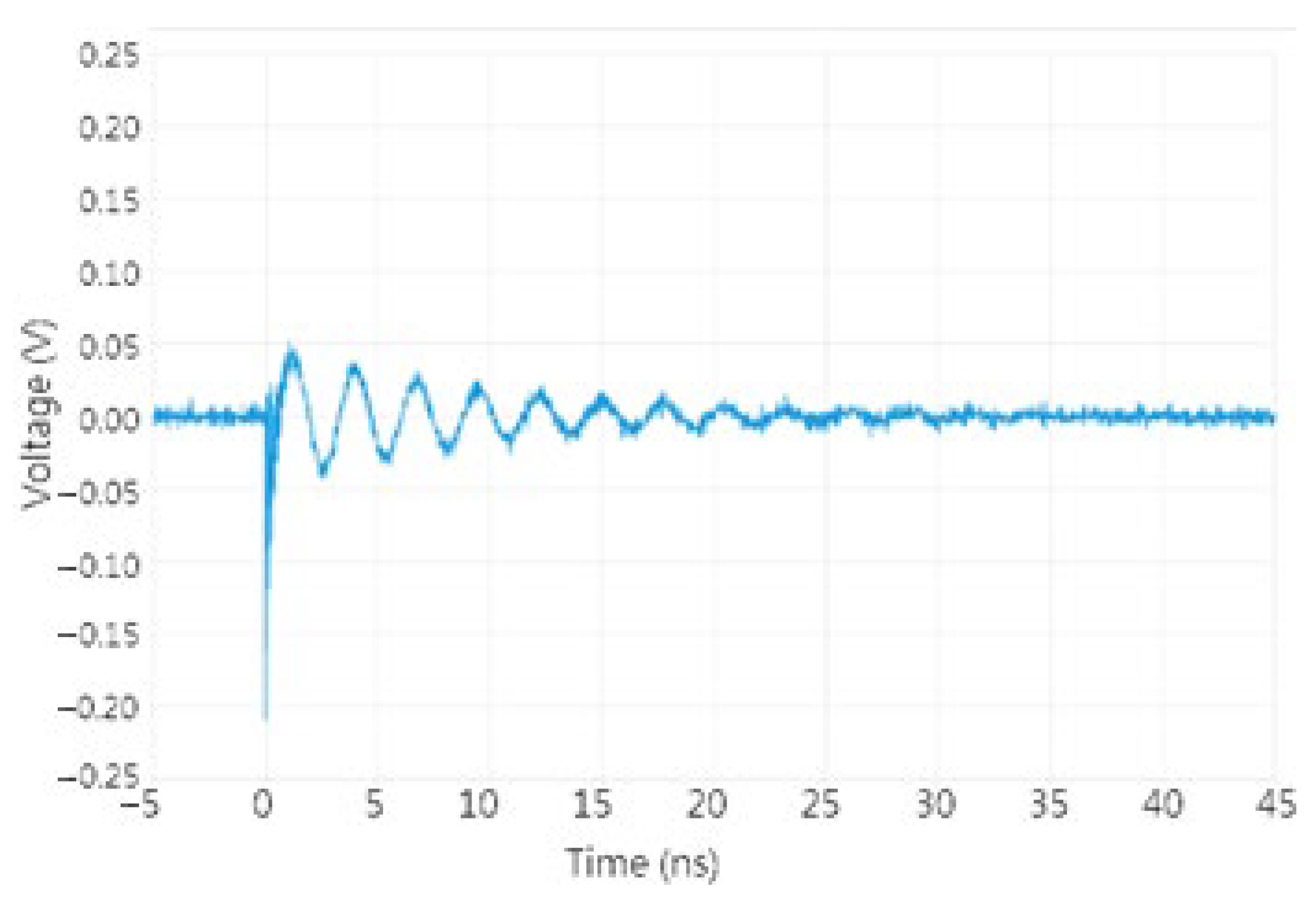
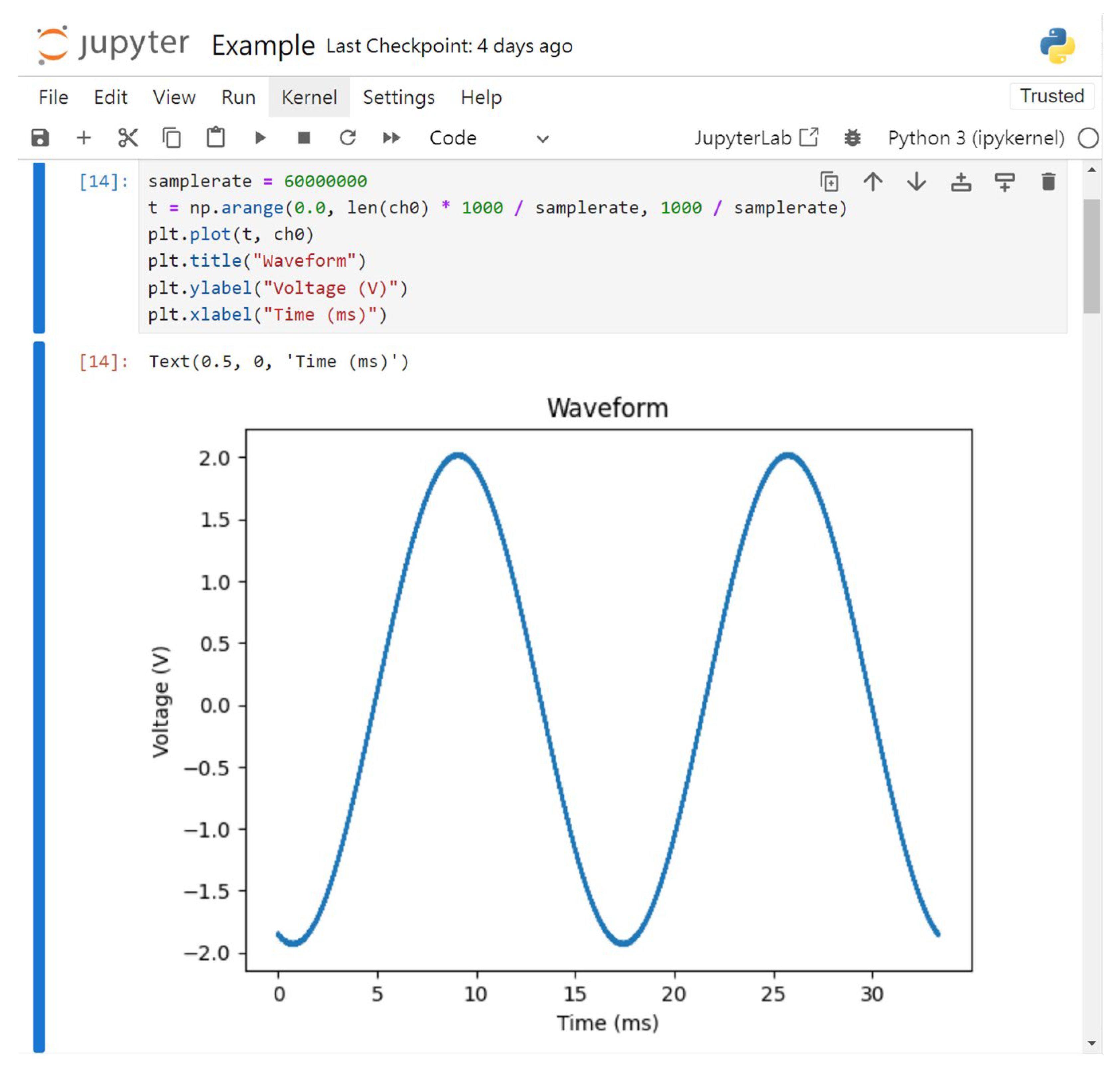
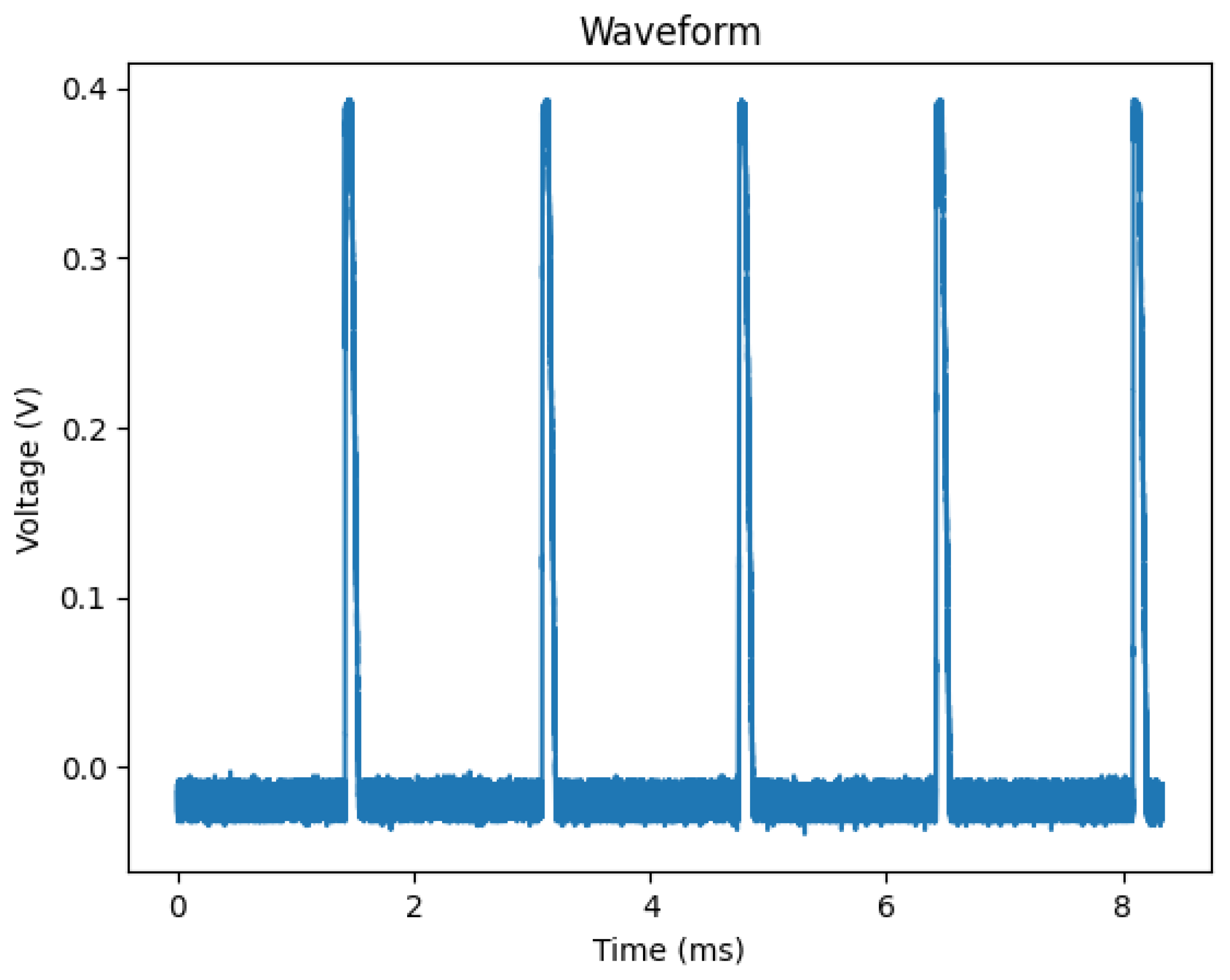
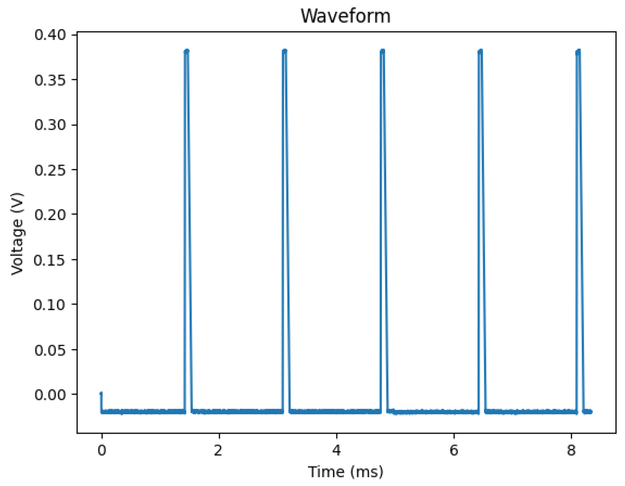
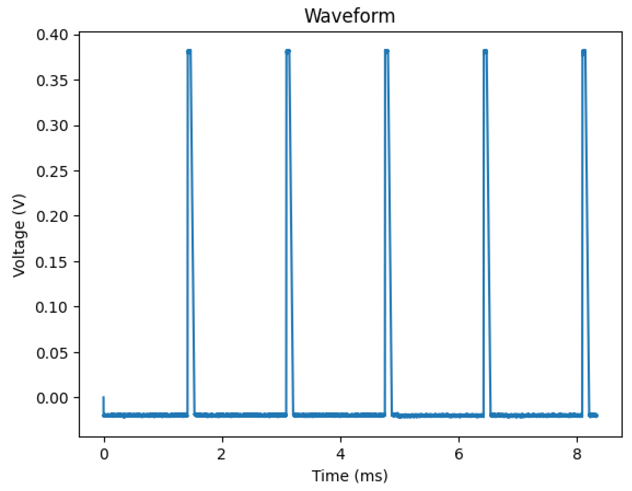
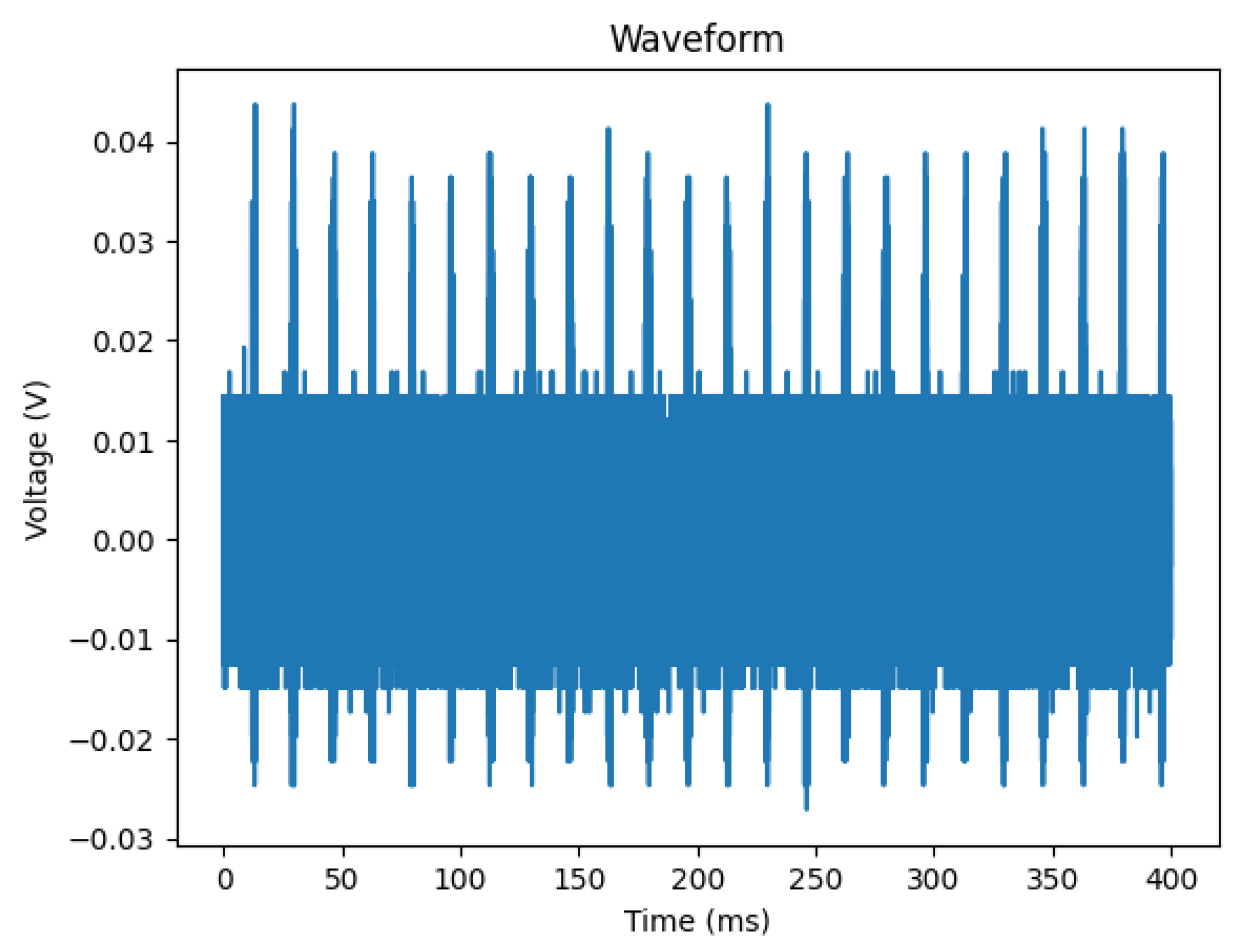
2.2.2. Discharge Waveform Measurement

The expert system for diagnosing damage to substation transmission and transformation equipment focuses on the online recording of raw discharge waveforms for oil-immersed transformers, as shown in Figure 7. It utilizes noise-suppression techniques and improves the identification rate of PD to ensure the reliable operation of the transmission and transformation equipment, reduce maintenance costs, enhance safety, ensure a stable power supply, and prevent power interruptions caused by unknown faults. PD is an important indicator for assessing the insulation health of substation transmission and transformation equipment. Continuous PD may lead to further aging or damage of insulation materials, thereby increasing the risk of equipment failure.

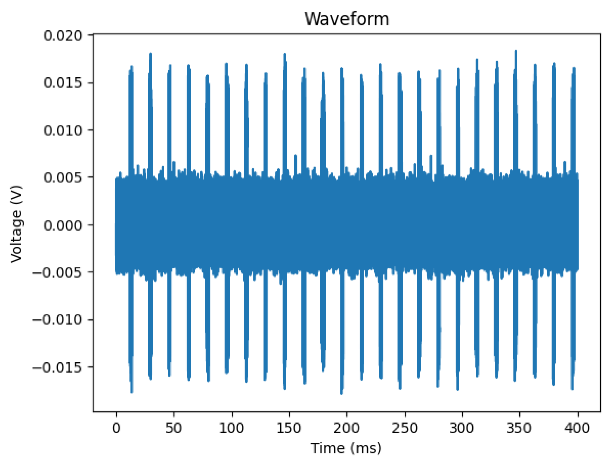
2.2.3. Noise-Suppression Technology

The noise-suppression technique is applied in the design planning of the raw discharge waveform-detection system for PD. It is a method and technology used to reduce or eliminate unnecessary signals, interference, or background noise. Filtering noise in the input of the analog-to-digital converter (ADC) is a common but important problem. Such converters are used to convert analog signals into digital signals, but they may introduce various types of noise in the process.
Two main specified requirements for bandpass and bandstop filters are the cutoff frequency at −3 dB and the stopband frequency fN. The variability of the bandwidth and stopband frequency in the filter will change the behavior of the filter. Filters with adjustable bandwidth and stopband frequency are known as variable filters or adjustable filters, and they play a very important role in digital signal-processing applications. There are various designs for variable bandpass and bandstop filters, with one of the previously proposed designs in the literature suggesting replacing almost all delay elements in the digital low-pass prototype filter with second-order digital all-pass filters and then modifying the coefficients, which can be computationally complex [21,22].
To efficiently reduce computational complexity, one method is to use a Taylor series expansion of the transfer function coefficients, but truncating the approximated linear terms can degrade the filter’s amplitude–frequency response. Another computationally simpler method adjusts only the center frequency f0 while keeping the bandwidth constant and is designed primarily for narrowband digital filters. This method adjusts the bandwidth of variable filters based on the cutoff frequency fc of the digital low-pass prototype filter, resulting in a limited range of frequencies and increased complexity for higher-order filters.
Another significant issue to consider is that the design of most digital bandpass and bandstop filters using the center frequency f0, which is the geometric mean of the lower frequency fL and the upper frequency fU, applies primarily to analog filter design. It is well known that using the center frequency f0 for designing digital bandpass and bandstop filters has limitations because f0 is not the stopband frequency fN and is only an approximation for the design of narrowband digital filters.
The results of capturing high-frequency signals from the raw discharge waveform of PD are shown in Figure 8. It is evident from the figure that the signal levels contain high-frequency noise. Filters can be used to create low-pass filters at different output points, primarily designed to allow low-frequency components to pass through while reducing or blocking high-frequency components. A low-pass filter can filter out all frequency components above a certain specific cutoff frequency, allowing only components below that frequency to pass. This is included in various applications of analog-to-digital converters. Additionally, it can be used to construct various broadband filters with independently controllable lower and upper cutoff frequencies, as well as to ensure frequency doubling and one-third octave filter sets in the form of tunable bandpass filters. The main drawback of tunable filters based on typical filter sections is that they do not allow for high stability at high frequencies. Figure 9 shows the results of an RC filter.
Finite impulse response (FIR) filters are characterized by having a finite-length impulse response, where the input signal is convolved with a set of fixed coefficients to obtain the output signal. These filters can typically be designed with linear phase characteristics, where all frequency components of the signal pass through the filter at the same rate, effectively reducing phase distortion.
The method presented in this paper uses variable IIR digital bandpass and bandstop filters by independently controlling α and β, two adjustable parameters, to achieve a −3 dB bandwidth bw and the stopband frequency fN. The parameter α originates from the frequency domain transformation from a low-pass to a low-pass filter and controls the −3 dB bandwidth. The parameter β controls the stopband frequency fN and is derived from the frequency-domain transformation from a low-pass to a high-pass filter. Digital bandpass and bandstop filters are obtained by transforming a half-band digital low-pass filter using digital-domain frequency transformations. Variable digital filters have fewer coefficients, which means there are fewer multipliers, adders, and delays in the implemented circuit compared to previous designs. The design steps of the method proposed in this paper are very simple in terms of computation, as it involves only two adjustable parameters. A new formula for the damping factor ζ with α and β is introduced, and the root locus of the second-order variable digital Butterworth bandpass and bandstop filters with a damping factor is analyzed. Figure 10 shows the results using an FIR filter.

3. Results

This study examined the performance of RC and FIR filters in suppressing noise in partial-discharge signals under the fixed conditions of a sampling rate of 20 Msps, a filter order of 20, and a cutoff frequency of 1.6 MHz. The analysis results are as follows:
The waveform of the original signal, shown in Figure 11, displays the typical characteristics of a partial-discharge signal, where the voltage changes show rapid pulse variations accompanied by a significant amount of high-frequency noise. The signal-to-noise ratio (SNR) at this stage was only 3.617 dB, indicating poor signal quality with a high level of noise, which poses challenges for subsequent signal analysis and identification.
After the application of the RC filter, as shown in Figure 12, the SNR improved to 9.223 dB. This indicates that the RC filter can effectively reduce high-frequency noise, although it may affect the shape and phase of the pulses to a certain extent. However, due to its analog nature, the RC filter may have difficulties in precisely controlling the cutoff frequency, and its performance can change over time with the variability of component tolerances.
With the use of the FIR filter, as shown in Figure 13, the SNR further increased to 9.968 dB, the highest among the three. As a digital filter, the FIR filter offers a superior noise-suppression effect and maintains the integrity and characteristics of the signal. The pulse shapes are clearer and smoother, which highlights the advantage of the FIR filter in maintaining a linear phase response, which is essential for preserving the authenticity of the signal.
The FIR filter demonstrates superior performance in the noise suppression of partial-discharge signals due to its inherent stability and consistent performance. Although FIR filters may require more computational resources, which should be considered when selecting a filter, they provide higher-quality signals for precise signal analysis. Conversely, if system resources are limited, the RC filter may be a more economical and practical choice. However, for the best signal quality, the FIR filter is the more appropriate option.

4. Conclusions

In this study, experiments were conducted using a partial-discharge signal simulator with three different levels of noise. Additionally, signal analysis and noise-suppression techniques were employed, utilizing a homemade data-acquisition module and digital signal processor (DSP) for analysis and computation. This approach not only reduces costs but also enhances computational performance. Compared to commercial PD detection systems like the PD700, the signal analysis and noise-suppression techniques effectively reduce noise and improve recognition rates. Experimental results demonstrate that the locally designed PD detection and analysis system can capture the discharge characteristics of PD and can be expanded as needed. Furthermore, the methods proposed in this study can also be applied to the recognition of PD in other types of high-voltage power equipment, thereby enhancing its functionality and contributions in industrial and commercial applications.

Author Contributions

Conceptualization, P.-C.T. and C.-K.C.; methodology, P.-C.T. and C.-K.C.; software, P.-C.T. and Y.-M.H.; formal analysis, P.-C.T., C.-K.C. and C.-C.K.; writing—original draft preparation, P.-C.T. and Y.-M.H.; writing—review and editing, P.-C.T., C.-K.C. and C.-C.K.; visualization, P.-C.T. and C.-K.C.; supervision, C.-C.K. All authors have read and agreed to the published version of the manuscript.

Funding

This research received no external funding.

Institutional Review Board Statement

Not applicable.

Informed Consent Statement

Not applicable.

Data Availability Statement

The data presented in this study are available on request from the corresponding author. The data are not publicly available due to restrictions.

Acknowledgments

Support for this research from the National Atomic Research Institute is gratefully acknowledged.

Conflicts of Interest

The authors declare no conflicts of interest.

References

  1. Petzold, F.; Schlapp, H.; Gulski, E.; Seitz, P.P.; Quak, B. Advanced solution for on-site diagnosis of distribution power cables. IEEE Trans. Dielectr. Electr. Insul. 2008, 15, 1584–1589. [Google Scholar] [CrossRef]
  2. Ma, H.; Chan, J.C.; Saha, T.K.; Ekanayake, C. Pattern recognition techniques and their applications for automatic classification of artificial partial discharge sources. IEEE Trans. Dielectr. Electr. Insul. 2013, 20, 468–478. [Google Scholar] [CrossRef]
  3. Chen, X.; Qian, Y.; Xu, Y.; Sheng, G.; Jiang, X. Energy estimation of partial discharge pulse signals based on noise parameters. IEEE Access 2016, 4, 10270–10279. [Google Scholar] [CrossRef]
  4. Zeng, F.; Wu, S.; Yang, X.; Wan, Z.; Tang, J.; Zhang, M.; Yao, Q. Fault diagnosis and condition division criterion of DC gas insulating equipment based on SF6 partial discharge decomposition characteristics. IEEE Access 2019, 7, 29869–29881. [Google Scholar] [CrossRef]
  5. Wang, D.; Du, L.; Yao, C.; Yan, J. UHF PD measurement system with scanning and comparing method. IEEE Trans. Dielectr. Electr. Insul. 2018, 25, 199–206. [Google Scholar] [CrossRef]
  6. Benzing, J.; Blokhintsev, I.; Patterson, C.; Loesch, A. Continuous OnLine Partial Discharge monitoring of medium voltage substations. In Proceedings of the Pulp and Paper Industry Technical Conference, Portland, OR, USA, 17–21 June 2012; pp. 1–7. [Google Scholar]
  7. Koch, H.J. Gas Insulated Substations; John Wiley & Sons Ltd. Press: Hoboken, NJ, USA, 2014; Volume 4, pp. 206–234. [Google Scholar]
  8. Piccin, R.; Mor, A.R.; Morshuis, P.; Girodet, A.; Smit, J. Partial Discharge Analysis of Gas Insulated Systems at High Voltage AC and DC. IEEE Trans. Dielectr. Electr. Insul. 2015, 22, 218–228. [Google Scholar] [CrossRef]
  9. Okamoto, T.; Uehara, H. Partial Discharge Current Measurements with Small Discharge Gaps Over Polyimide Film. IEEE Trans. Dielectr. Electr. Insul. 2023, 30, 158–164. [Google Scholar] [CrossRef]
  10. Ding, D.; Gao, W.; Liu, W. Influence of the Structure Dimension of GIS on the Partial Discharge. In Proceedings of the IEEE International Conference Condition Monitoring and Diagnosis, Bali, Indonesia, 23–27 September 2012; pp. 958–962. [Google Scholar]
  11. Wu, M.; Cao, H.; Cao, J.; Nguyen, H.L.; Gomes, J.B.; Krishnaswamy, S.P. An overview of state-of-the-art partial discharge analysis techniques for condition monitoring. IEEE Electr. Insul. Mag. 2015, 31, 23–35. [Google Scholar] [CrossRef]
  12. Ghorat, M.; Gharehpetian, G.B.; Latifi, H.; Hejazi, M.A. A new partial discharge signal denoising algorithm based on adaptive dual-tree complex wavelet transform. IEEE Trans. Instrum. Meas. 2018, 67, 2262–2272. [Google Scholar] [CrossRef]
  13. Guozhi, Z.; Zhang, X.; Xingrong, H.; Jia, Y.; Tang, J.; Yue, Z.; Yuan, T.; Zhenze, L. On-line monitoring of partial discharge of less-oil immersed electric equipment based on pressure and UHF. IEEE Access 2019, 7, 11178–11186. [Google Scholar] [CrossRef]
  14. Zhang, J.J. The Technology and Application of High Voltage Discharge Ultraviolet Detection; China Electric Power Press: Beijing, China, 2009. [Google Scholar]
  15. Yao, P.; Zheng, H.; Yao, X.S.; Ding, Z. A method of monitoring partial discharge in switchgear based on ozone concentration. IEEE Trans. Plasma Sci. 2019, 47, 654–660. [Google Scholar] [CrossRef]
  16. CIGRE WG D1.33. Guide for Electrical Partial Discharge Measurements in Compliance to IEC 60270; Technical Brochure 366, Electra; CIGRE: Paris, France, 2008; Volume 60, No. 241. [Google Scholar]
  17. Upton, D.W.; Saeed, B.I.; Mather, P.J.; Sibley, M.J.; Lazaridis, P.I.; Mistry, K.K.; Glover, I.A.; Torres Filho, F.; Tachtatzis, C.; Atkinson, R.C.; et al. Low power radiometric partial discharge sensor using composite transistor-reset integrator. IEEE Trans. Dielectr. Electr. Insul. 2018, 25, 984–992. [Google Scholar] [CrossRef]
  18. Adzis, Y.Z.; Izzati, W.A.; Adzis, Z. Modeling of partial discharge mechanisms in solid dielectric material. Int. J. Eng. Innov. Technol. 2012, 1, 315–320. [Google Scholar]
  19. Govindarajan, S.; Ardila-Rey, J.A.; Krithivasan, K.; Subbaiah, J.; Sannidhi, N.; Balasubramanian, M. Development of Hypergraph Based Improved Random Forest Algorithm for Partial Discharge Pattern Classification. IEEE Access 2021, 9, 96–109. [Google Scholar] [CrossRef]
  20. Gu, F.-C.; Chang, H.-C.; Hsueh, Y.-M.; Kuo, C.-C.; Chen, B.-R. Development of a high-speed data acquisition card for partial discharge measurement. IEEE Access 2019, 7, 140312–140318. [Google Scholar] [CrossRef]
  21. Phuoc, N.S. Variable IIR Digital Band-Pass and Band-Stop Filters. In Proceedings of the 2018 2nd International Conference on Imaging Signal Processing and Communication (ICISPC), Kuala Lumpur, Malaysia, 20–22 July 2018; pp. 132–137. [Google Scholar]
  22. Samoylov, L.; Prokopenko, N.; Denisenko, D. Dynamic Errors of Butterworth Band-Pass Filters in Analog-digital Control and Monitoring Systems. In Proceedings of the 2022 International Russian Automation Conference (RusAutoCon), Sochi, Russian, 4–10 September 2022; pp. 128–133. [Google Scholar] [CrossRef]
Figure 1. Original partial discharge waveform.
Applsci 14 01195 g001
Figure 2. AM3358 board.
Applsci 14 01195 g002
Figure 3. AD9226 analog-to-digital converter.
Applsci 14 01195 g003
Figure 4. Xilinx XC6SLX16-2CSG324.
Applsci 14 01195 g004
Figure 5. Embedded system.
Applsci 14 01195 g005
Figure 6. Jupyter Notebook UI.
Applsci 14 01195 g006
Figure 7. Simulated discharge waveform of power transmission transformation equipment.
Applsci 14 01195 g007
Figure 8. Original discharge simulation waveform.
Applsci 14 01195 g008
Figure 9. Simulation waveform noise suppression results using RC filtering.
Applsci 14 01195 g009
Figure 10. Simulation waveform noise suppression results using FIR.
Applsci 14 01195 g010
Figure 11. Partial discharge waveform acquisition using self-develop hardware.
Applsci 14 01195 g011
Figure 12. Partial discharge waveform after RC filter.
Applsci 14 01195 g012
Figure 13. Partial discharge waveform after FIR filter.
Applsci 14 01195 g013
Disclaimer/Publisher’s Note: The statements, opinions and data contained in all publications are solely those of the individual author(s) and contributor(s) and not of MDPI and/or the editor(s). MDPI and/or the editor(s) disclaim responsibility for any injury to people or property resulting from any ideas, methods, instructions or products referred to in the content.

