Article

Design and Signal-Decoding Test Verification of Dual-Channel Round Inductosyn Decoding Circuit

National Key Laboratory of Aerospace Mechanism, College of Astronautics, Nanjing University of Aeronautics and Astronautics, Nanjing 211106, China
*
Author to whom correspondence should be addressed.
Appl. Sci. 2024, 14(21), 9801; https://doi.org/10.3390/app14219801
Submission received: 13 October 2024 / Revised: 22 October 2024 / Accepted: 24 October 2024 / Published: 27 October 2024

Abstract

:
During the in-orbit operation of spacecraft, permanent magnet synchronous motors are commonly used as power sources in the drive mechanisms of solar panel arrays and the high-precision servo control systems based on satellites. Apart from the performance of the motors themselves and the software control algorithms, the accuracy of the entire control system is also influenced by angle sensors used to detect the rotor position of the motors. As a high-precision angular measuring instrument, the inductosyn possesses excellent environmental adaptability and long service life. Effectively utilizing the inductosyn can greatly enhance the performance of servo control systems. To address the complexity of the decoding process for dual-channel round inductosyn-to-digital converters, this paper proposes a design of the decoding circuit for dual-channel round inductosyn based on the parallel-synchronization decoding method of two AD2S1210 Resolver-to-Digital Converter (RDC) decoding chips. The decoding circuit amplifies the excitation signal outputted by the AD2S1210 for driving the round inductosyn, and processes the sine and cosine induction signals outputted by the round inductosyn through filtering, amplification, and other methods; by using analog circuitry, the output signals of the dual-channel round inductosyn are processed to meet the input requirements of the AD2S1210. Finally, through both the Multisim (circuit simulation software Version 14.1) simulation and physical experiments, it was verified that the decoding circuit designed in this paper could process the input/output signals of the dual-channel round inductosyn and AD2S1210, and successfully decoded the analog induction signal of the round inductosyn. This greatly simplifies the signal decoding process for the dual-channel round inductosyn.

1. Introduction

As the demand for the rapid tracking and precise positioning of servo control systems on orbiting spacecraft continues to increase, especially for high-precision spacecraft, the minute vibrations introduced by moving components can have a significant impact on payload resolution [1]. Considering the significant cost of energy supply for spacecraft in orbit, high-efficiency energy conversion and stable permanent magnet synchronous motor drive-control systems are widely utilized [2]. To achieve the precise vector control of permanent magnet synchronous motors, in addition to excellent control algorithms, angle sensors that can provide rapid and accurate feedback of the motor rotor position are also crucial [3,4,5,6]. Common angle sensors include circular grating, coding disk, encoders, resolvers, and inductosyn. Among them, encoders can directly output pulse signals containing angle information for communication with microprocessors, making them the simplest to apply, although their precision ceiling is lower compared to other sensor types [7]. Gratings and coding disks are typically used in servo control systems with high precision requirements, but have strict environmental requirements and complex assembly processes, leading to high maintenance costs [8]. The round inductosyn is a type of high-precision angular displacement sensor based on the principle of electromagnetic induction [9,10]. Its operation principle is similar to that of a resolver [11], but with more pole pairs, sometimes including coarse and fine channels. Its accuracy significantly surpasses that of a resolver. Meanwhile, the round inductosyn requires lower installation precision, exhibits resistance to shock and vibration, boasts excellent environmental adaptability [12], and offers a long operational lifespan. It can be utilized in scenarios where gratings are unsuitable, such as high-orbit weather satellites. As a result, the round inductosyn is increasingly being incorporated into high-precision servo control systems in aerospace applications [13].
The signals directly input/output by the round inductosyn are analog signals, which need to be decoded before being converted into digital angle quantities for reception by the subsequent system microprocessor, achieving angle acquisition for the control system [14,15,16,17]. For the decoding-circuit design of the round inductosyn, the mainstream approach involves utilizing microprocessors such as FPGA (Field-Programmable Gate Array) and DSP (Digital Signal Processor) in conjunction with peripheral A/D sampling circuits to convert the output signals of the round inductosyn into digital quantities. In the software algorithm, trigonometric transformations such as inverse tangent are employed to calculate the angle information [18]. This method requires hardware design for the input/output signal processing circuitry of the round inductosyn, as well as software algorithm design for the microprocessor; even with the help of artificial intelligence technology [19,20,21], it is difficult to achieve a balance between software and hardware design.
Due to the similarity in principles between the round inductosyn and resolvers, this paper draws inspiration from resolver decoding techniques to design the decoding circuit for the round inductosyn. Currently, RDC decoding chips are commonly used to decode resolvers in servo control systems [22,23,24]. However, the round inductosyn have certain driving capability requirements for excitation signals, and the induced signals mostly consist of dual-channel multi-output signals, with very small amplitudes typically in the range of tens of millivolts. Existing resolver decoding circuits are primarily designed for single-channel excitation and single-channel output modes, making it challenging to adapt the signal output/input specifications to the round inductosyn. Therefore, this paper proposes a decoding circuit design based on a dedicated resolver decoding chip, the AD2S1210, tailored to the signal characteristics of dual-channel round inductosyn. This circuit processes both excitation and induced signals, utilizing two AD2S1210 chips to synchronously decode the coarse and fine channels of the dual-channel round inductosyn. The proposed design is validated through simulation and physical circuit experiments.

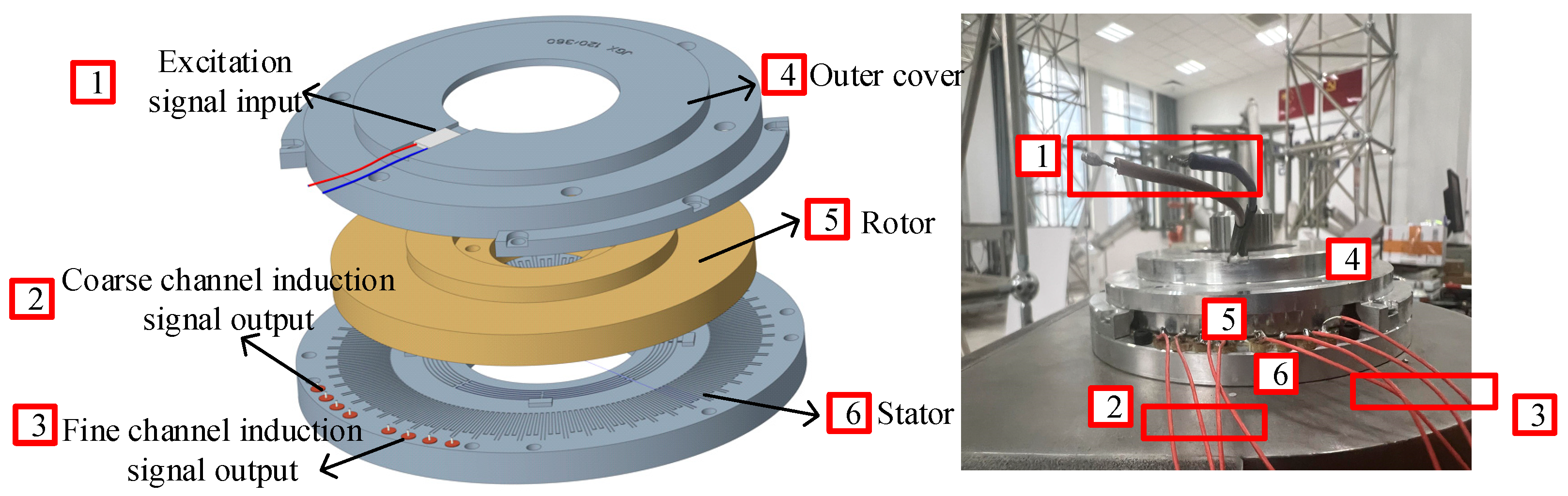
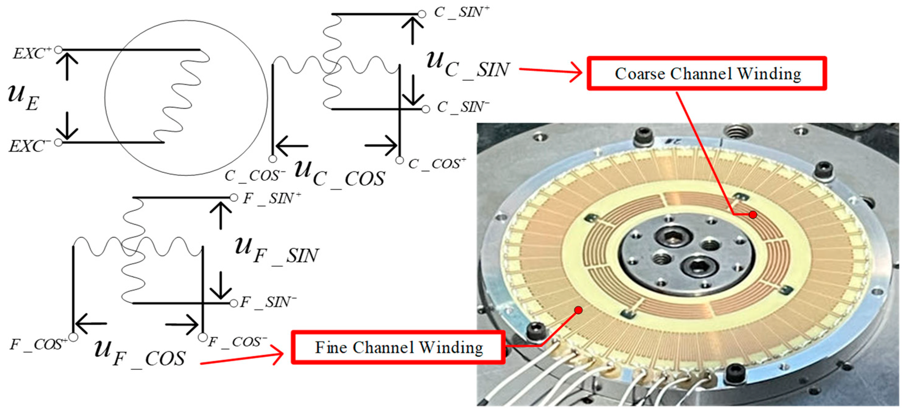
2. Principle of the Dual-Channel Round Inductosyn

The round inductosyn is a multi-pole induction device. When an excitation signal is input from the outside, the electromagnetic induced signals between the stator and rotor plane windings change with displacement, producing alternating electromotive forces that vary sinusoidally and cosinusoidally. When one phase winding is at the zero position, the other phase winding outputs the maximum electromotive force. Through the output of the two-phase electromotive forces, the angular position can be clearly reflected at any position within one cycle. With the appropriate decoding circuit, the current angular position can be detected. This paper describes the JGX120/360 type dual-channel round inductosyn developed by Changzhou Weinengda Precision Machinery Co., Ltd., Changzhou, China. It has a speed ratio of 1:180 and a structure as shown in Figure 1, consisting of an outer cover, rotor, and stator from top to bottom. The two wirings above the outer cover are the differential inputs for the excitation signal, while the eight terminals on the stator correspond to the differential outputs of the sine- and cosine-induced signals for the coarse channel and fine channel, respectively.
The dual-channel round inductosyn operates based on the principle of mutual inductance between the alternating magnetic field and the coil windings. The electrical schematic diagram is shown in Figure 2. EXC+ and EXC are the input terminals for the excitation signal of the round inductosyn, C_SIN+ and C_SIN are the terminals for the coarse-channel sine winding on the stator, C_COS+ and C_COS are the terminals for the coarse-channel cosine winding on the stator, F_SIN+ and F_SIN are the terminals for the fine-channel sine winding on the stator, and F_COS+ and F_COS are the terminals for the fine-channel cosine winding on the stator.
When the input is a sine excitation signal u E = U sin ( w t ) , the electrical signals induced by the coarse- and fine-channel windings are shown in Equation (1), where U and w are the amplitude and angular frequency of the excitation signal; k C and k F are the signal transformation ratios for the coarse and fine channels, respectively; u C _ S I N and u C _ C O S are the sine- and cosine-induced signals at the stator coarse-channel winding, and u F _ S I N and u F _ C O S are the sine- and cosine-induced signals at the stator fine-channel winding; θ C and θ F are the angles of the stator and rotor, respectively, and w is the angular frequency of the excitation signal.
u C _ S I N = k C U sin ( w t ) sin θ C u C _ C O S = k C U sin ( w t ) cos θ C u F _ S I N = k F U sin ( w t ) sin θ F u F _ C O S = k F U sin ( w t ) cos θ F

3. Decoding-Circuit Hardware Design

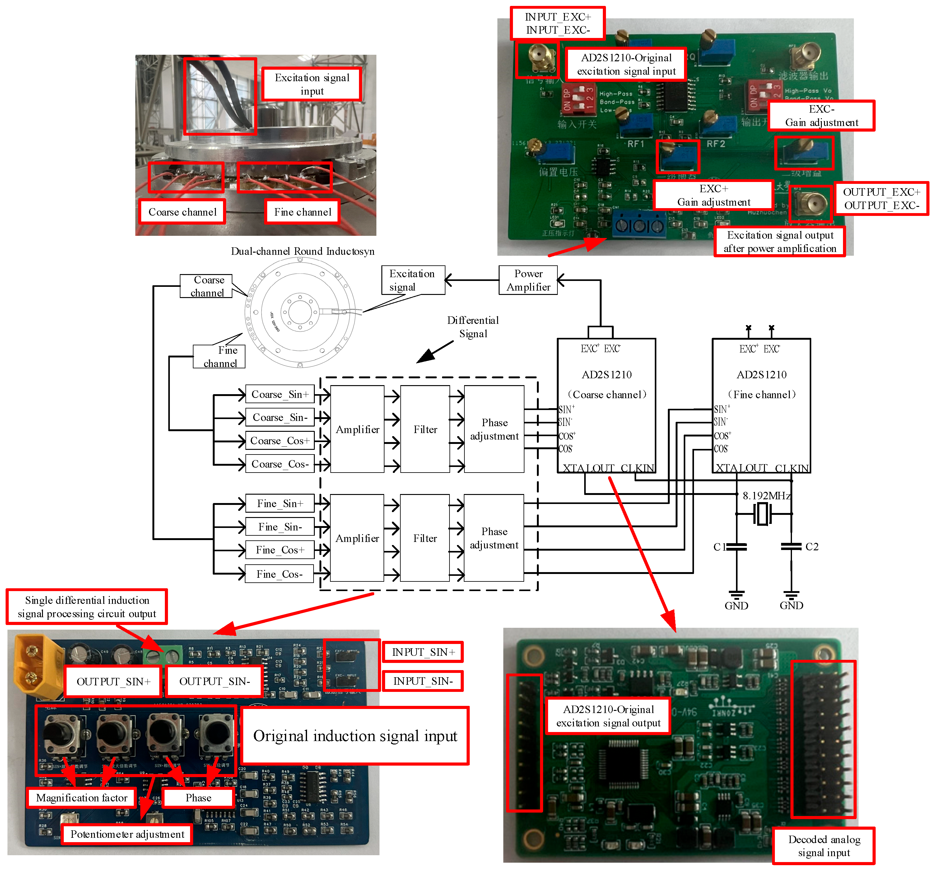
3.1. Hardware Architecture of Decoding Circuit

The overall hardware architecture diagram of the decoding circuit is shown in Figure 3. The paper selects ADI’s RDC decoding chip AD2S1210 as the core decoding chip of the decoding circuit. Similar to the widely used AD2S80 chip, it is based on the Type-II tracking loop principle and is commonly used in resolver systems to convert the rotor’s angular position into digital data. This digital data are then sent to the system microprocessor to decode the angle position information. Compared to the AD2S80, the AD2S1210 has a smaller size and a more simplified peripheral circuit configuration. It is powered by a single +5 V power supply instead of dual power supplies. Additionally, when configuring different resolution modes, only adjusting the chip’s register configuration is sufficient; no need to modify the circuit hardware. This greatly simplifies the circuit design and debugging work.
The JGX120/360 dual-channel round inductosyn developed by Changzhou Weinengda Precision Machinery Co., Ltd., which is used in this paper, is a dual-channel round inductosyn with one excitation input and two channel-induced signal outputs. To achieve synchronized decoding for the dual-channel round inductosyn, as each AD2S1210 chip can only take one set of sine and cosine differential signals, the paper adopts a parallel connection method where two AD2S1210 chips share a common clock signal. One chip is selected for outputting the excitation signal, while the output pin of the other chip remains floating. Each of the two AD2S1210 chips decodes the position information of the coarse and fine channels of the inductosyn and converts it into digital signals. According to the AD2S1210 chip’s datasheet, when powered by +5 V, the chip can provide a typical differential excitation signal of 7.2 Vp-p for the round inductosyn. However, the drive capability of this signal may not meet the excitation signal input requirements of the round inductosyn, necessitating power amplification processing. According to the operation manual of the dual-channel round inductosyn, it is known that the range of the sine excitation signal should be between 6 Vp-p and 9 Vp-p, with a frequency around 10 KHz, to be in the optimal working state. Taking the example of an input sine excitation signal of 7.2 Vp-p and 10 KHz, the coarse-channel-induced signal of the round inductosyn was measured at 10 mVp-p and 10 KHz, while the fine-channel-induced signal was measured at 20 mVp-p and 10 KHz. According to the AD2S1210’s datasheet, the input range for the sine and cosine differential signals is 2.3 Vp-p to 4.0 Vp-p. Therefore, it is necessary to amplify and filter the original induced signals. After the induced signal passes through the amplifier and filter, it will introduce a certain phase shift. However, as the phase difference between the input signal and excitation signal of the AD2S1210 chip needs to be less than 44°, a phase adjustment should be added to the decoding circuit to correct the signal phase. Based on the above information, the design specifications for the decoding circuit can be summarized as shown in Table 1.

3.2. Design of Power Amplification Circuit for Excitation Signal

The differential excitation signal generated by the decoding chip AD2S1210 is output from the EXC+ and EXC− pins, with a typical value of 7.2 Vp-p. The amplitude of the signal meets the input requirements for the excitation signal of the round inductosyn used in this paper. However, the excitation signal current directly output by the AD2S1210 is too small, resulting in poor driving effect on the round inductosyn. To address the issue of low output current, this paper builds a proportional amplification circuit based on the high-output-current operational amplifier AD8397. By increasing the output current of the excitation signal and slightly boosting the signal’s amplitude, the driving capability of the excitation signal on the round inductosyn is enhanced. The schematic diagram of the excitation signal power amplification circuit is shown in Figure 4.
In Figure 4, resistors R1, R2, R3, and R4 are used to set the amplification factor, capacitors C1 and C2 are for filtering to remove high-frequency components from the excitation signal, and potentiometer R5 is used to set the in-phase input voltage or bias voltage of AD8397. By adjusting the bias voltage, the average voltage or common-mode voltage of the output at terminals OUTPUT_EXC+ and OUTPUT_EXC− of the power amplification circuit can be adjusted. The calculation relationships between the bias voltage V b , input voltage V I , output voltage V o , and various component parameters are shown in Equation (2).
V b = R 4 R 4 + R 5 V R E F V O = R 1 + R 2 R 1 V b R 2 R 1 V I
V R E F is used to configure the external input voltage for bias voltage. Adjusting the appropriate common-mode voltage can help avoid signal clipping or distortion. When the common-mode voltage is approximately half of the operational amplifier’s supply voltage, the signal can obtain a larger amplitude output.

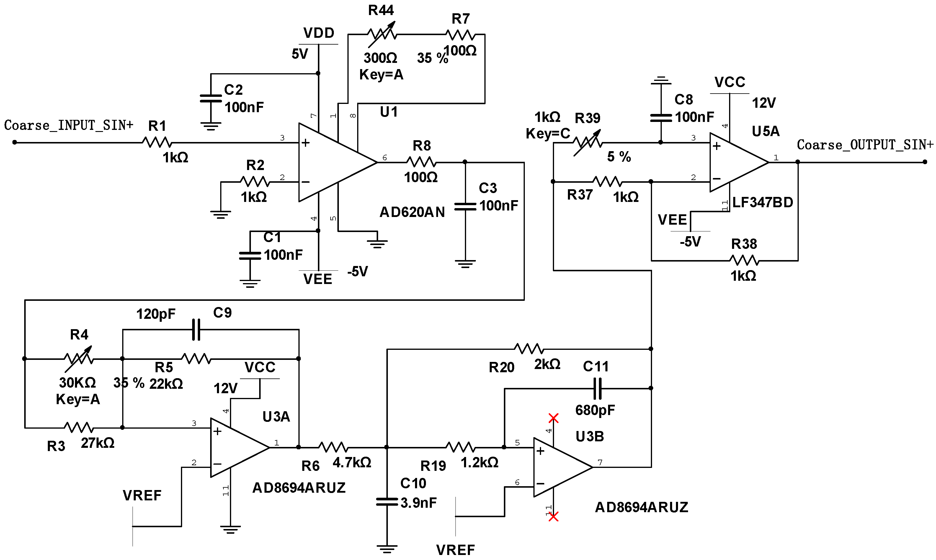
3.3. Design of Induced-Signal Processing Circuit

The induced signal is extracted from the wiring terminals on the stator of a round inductosyn, with two channels, namely coarse and fine. Each channel has four terminal outputs for the induced signal, providing differential signals for sine and cosine. Therefore, for the processing circuit of the induced signal, it is necessary to design eight sets of circuits that meet the design specifications to process the output signals into signals that meet the input requirements of AD2S1210. For the induced-signal processing circuit, a design process is adopted that involves amplification, filtering, and phase adjustment to maximize the preservation of the original characteristics of the induced signal. The processing circuits for the eight sets of differential signals in the coarse and fine channels are essentially the same. However, due to the different output amplitudes of the coarse- and fine-channel-induced signals, as well as minor errors between components, slight adjustments in the values of some resistors and capacitors may be necessary. Additionally, adjustable resistors are used for some components, eliminating the need to modify the hardware circuit when individually debugging each signal in the future. Figure 5 shows the schematic diagram of the induced-signal processing circuit. It only presents the processing circuit for one channel of the coarse-channel SIN+ induced signal, with the other signal processing circuits being essentially the same as this one.
The first stage of the induced-signal processing circuit is an amplification circuit. In this paper, we use the high-precision instrumentation amplifier AD620 produced by ADI to build the circuit. The AD620 features low DC offset, low drift, low noise, high common-mode rejection ratio, and high input impedance. It has a gain range of 1–10,000, and the external circuit configuration is very simple. Gain adjustment can be achieved by changing external resistors. In Equation (3), G represents gain, and R g represents the adjusting resistor.
G = 49.4 k Ω R g + 1
To amplify the differential signal of the coarse channel, which is 20 mVp-p, to meet the specified range of 3.2 Vp-p ± 0.5 V, a gain setting between 140 and 180 is required. However, considering the impact of subsequent filtering circuits and phase adjustment circuits on the overall gain, some adjustment margin should be left for the amplification circuit. Therefore, this paper adopts a design of a fixed resistor in series with a potentiometer as the gain adjustment resistor. This is shown in the connection between pins 1 and 8 of U1 in the schematic diagram of the induced signal processing circuit, as shown in Figure 5. For the coarse-channel SIN− and COS+/COS−, the peripheral configuration circuit of AD620 is the same. However, since the original induced-signal output amplitude of the fine channel is approximately half that of the coarse channel, it is necessary to appropriately modify the fixed resistor and potentiometer pairing in the gain adjustment section to increase the gain.
Due to the electromagnetic induction process between the stator and rotor of the round inductosyn, noise signals will inevitably be generated. Although the amplification circuit can filter out noise to a certain extent, noise will also be introduced during the signal transmission process. Excessive noise can cause more spikes in sine signals, and in severe cases, it can alter the sine characteristics of the signal. Therefore, the second stage of the induced-signal processing circuit is a filtering circuit. The filtering circuit is built around the AD8694 operational amplifier produced by Analog Devices (ADI). Two operational amplifiers from the AD8694 chip are used to configure the peripheral circuit. The filtering circuit is designed as a third-order Butterworth low-pass filter, as shown in the circuit schematic in Figure 5. By adjusting the potentiometer R4 at the inverting input of the lower-left operational amplifier AD8694 in the diagram, the gain of the filter can be finely adjusted within the range of 0.5–0.8.
The final stage of the decoding circuit is the phase adjustment circuit. According to the previous description, the phase difference between the excitation signal and the sine-/cosine-induced signals of the AD2S1210 should be less than 44°. Due to the fact that the round inductosyn is not a purely resistive component, and considering the presence of amplification and filtering circuits, the induced-signal output after processing is inevitably prone to phase shift compared to the excitation signal. This can significantly impact the decoding accuracy of the AD2S1210. Therefore, in the final stage of the decoding circuit, a notch filter based on LF347 has been designed. Through this stage, it is theoretically possible to achieve a phase shift of the signal between 0 and 180°. In the schematic diagram of the induced-signal processing circuit shown in Figure 5, by adjusting the potentiometer R39 at the inverting input of the LF347, it is possible to achieve the phase shifting of the signal to the desired phase.

4. Experimental and Analysis

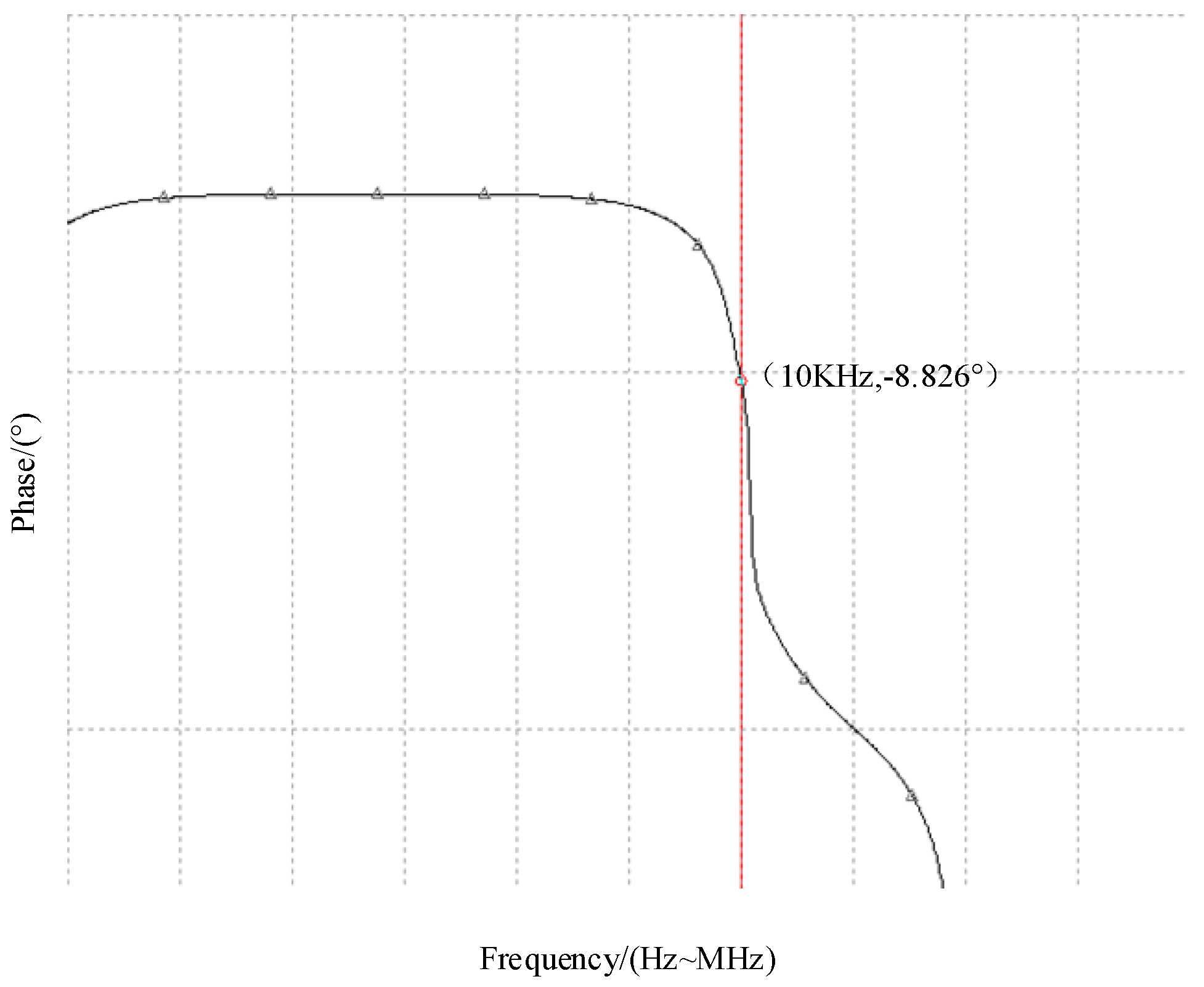
4.1. Multisim Simulation Experiment

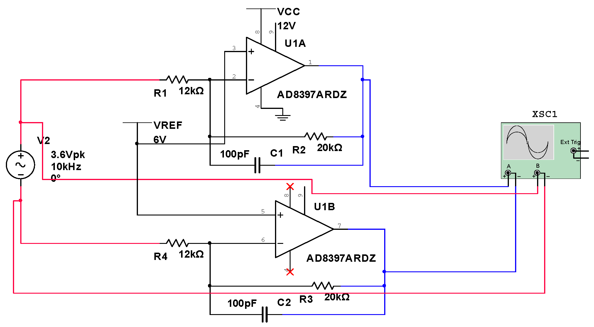
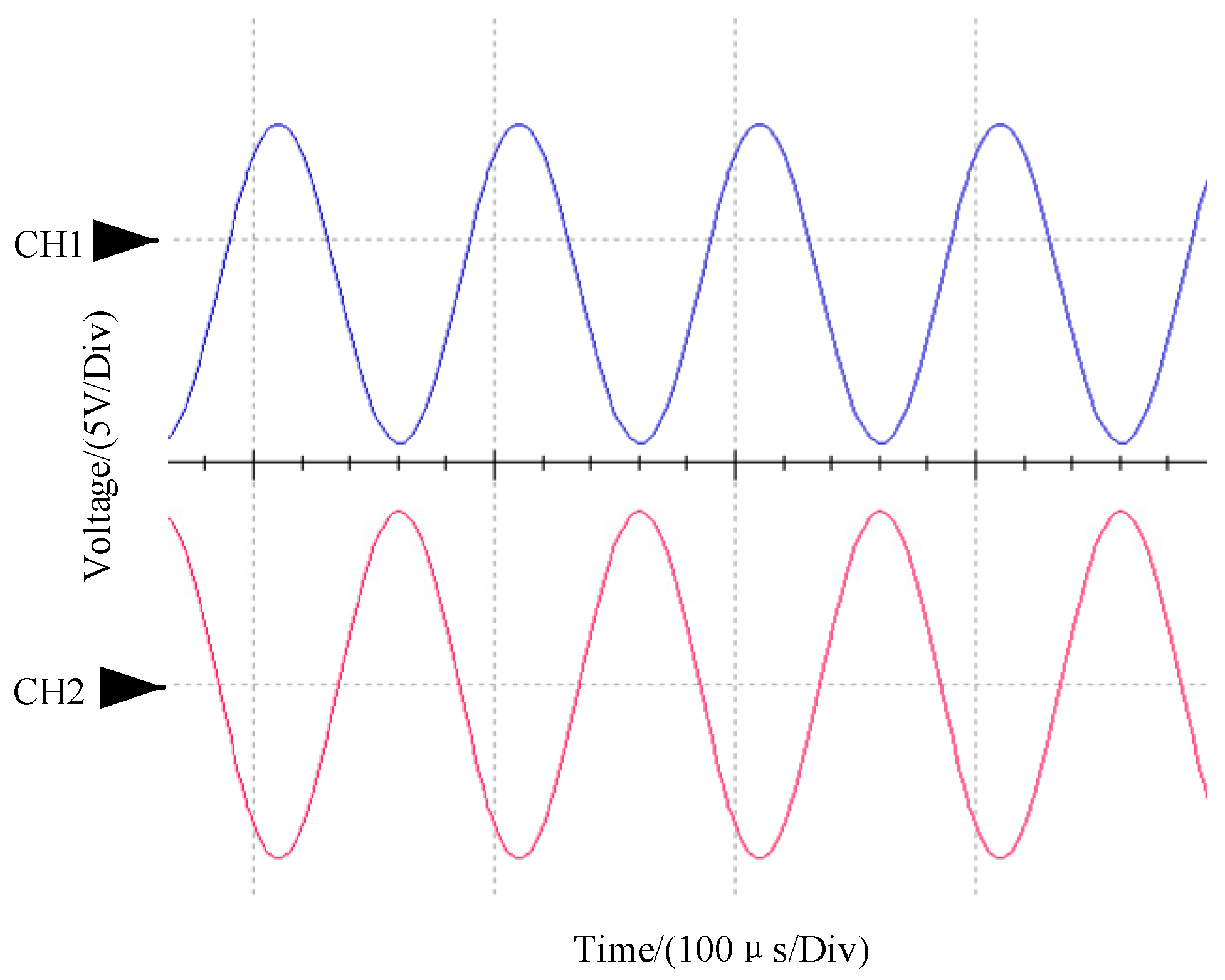
4.1.1. Power-Amplifier Circuit—Multisim Simulation Experiment

In the Multisim simulation software version 14.1, the simulation verification of the excitation-signal power-amplification circuit is conducted. The excitation input signal is set to a 7.2 Vp-p, 10 kHz sine wave with a phase offset of 0°. AD8397ARDZ is a dual-channel operational amplifier. In the Multisim simulation, a +12 V power supply can be applied to the power pin of one of the operational amplifiers to ensure normal operation. The V R E F voltage is set to 6 V. The other component parameters and circuit connections are as shown in Figure 6.
In Figure 6, XSC1 is a dual-channel oscilloscope used to observe the waveform of the input excitation signal before and after passing through the power-amplification circuit. The simulation results are shown in Figure 7.
The waveforms, from top to bottom, correspond to CH1 and CH2 represents the original excitation signal and the signal after power amplification, respectively. The peak-to-peak values of the signals are 7.16 V and 7.75 V, with frequencies both close to 10 kHz. From the simulation results, it can be observed that the excitation signal undergoes a slight increase in amplitude after power amplification, while maintaining good sinusoidal characteristics. The phase of the amplified signal is opposite to that of the input waveform. Overall, the results align with the theoretical expectations and meet the design criteria of the decoding circuit for the excitation signal.

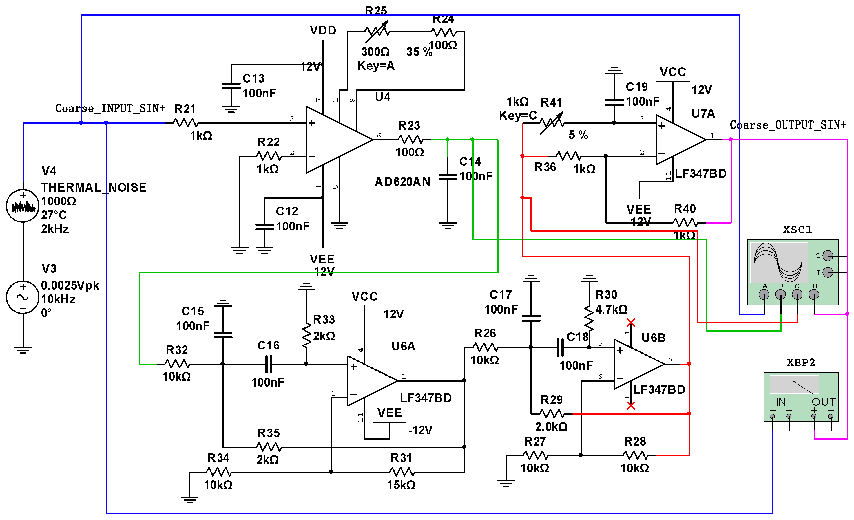
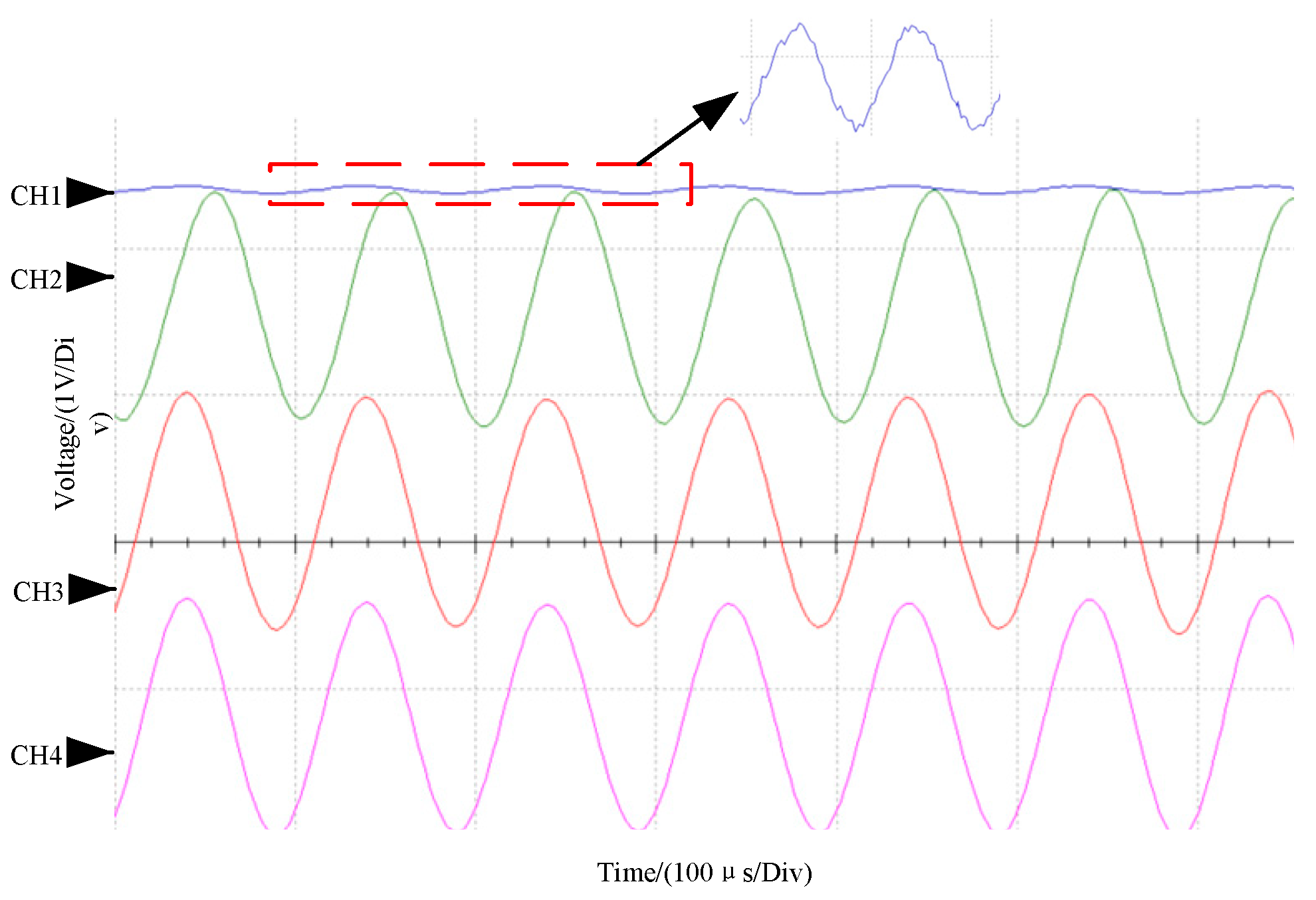
4.1.2. Induced-Signal Processing Circuit—Multisim Simulation Experiment

For the simulation experiment of the induced-signal processing circuit, taking the SIN+ terminal of the coarse channel as an example, with an an input of 5 mVp-p, 10 kHz sine wave signal as the original induced signal. Additionally, to verify the effectiveness of the filtering circuit, some high-frequency noise is added to the input signal. Simulate the actual state of the original induced signal with noise interference. The parameters of each component in the simulation and the circuit diagram connections are shown in Figure 8.
In Figure 8, XSC1 is a four-channel oscilloscope, and the waveform recording results of the oscilloscope are shown in Figure 9. XBP2 is a Bode plot tester, and the phase–frequency characteristics curve of the induced-signal processing circuit recorded by XBP2 is shown in Figure 10. The signals and amplitudes corresponding to each channel in Figure 9 are listed in Table 2.
After adding some noise in the simulation, it can be observed that the waveform of CH1 has more spikes, but the overall sinusoidal characteristic is evident. It is close to the original induced-signal output from the SIN+ terminal of the round inductosyn, with an amplitude of approximately 5 mV peak-to-peak and a frequency of around 10 kHz. From the waveform of CH2, it can be seen that after amplification, the original induced signal is at 1.5 V peak-to-peak, and many of the spikes in the waveform have been reduced, although some irregularities still remain.
As shown in the waveform of CH3, after the signal has passed through filtering, it has become a relatively standard sinusoidal signal. Due to the phase shift caused by the first two stages of the circuit, the waveform in CH3 does not differ significantly in phase from the original induced signal. As shown in Figure 10, the phase–frequency characteristic curve from the Bode plotter in the Multisim software indicates that the phase shift introduced by the two-stage amplification and filtering circuit for a 10 kHz signal is −8.826°.
According previous description, the excitation signal generated by AD2S1210 undergoes an inversion of 180° after passing through the power amplifier. When this is combined with the phase shift of the filtering and amplification circuit, and further adjusted by the phase-shift circuit, it can be tuned to achieve a phase difference of within 44° compared to the original excitation signal, as shown in the waveform in Figure 9, with an amplitude of 1.6 Vp-p. The simulation results meet the design requirements.

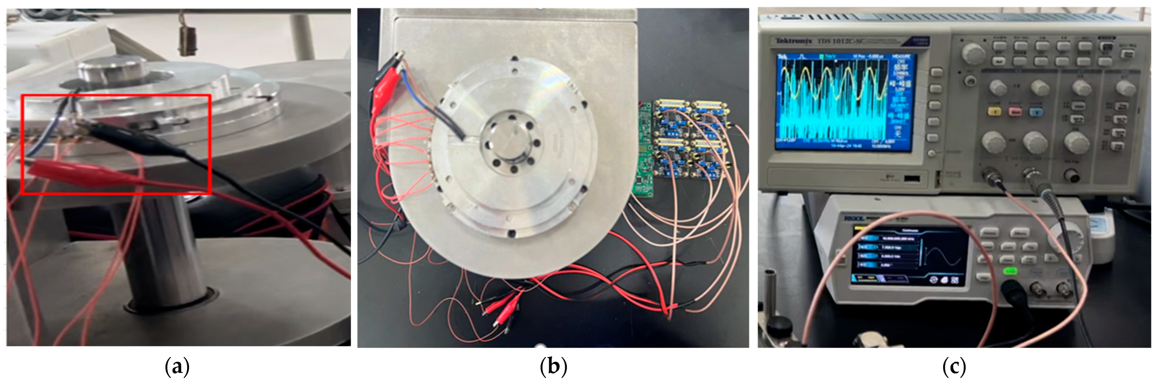
4.2. Physical Experiment

To further validate the feasibility of the proposed solution, a physical platform as depicted in Figure 11 was constructed to conduct experimental tests on the demodulation circuit.

4.2.1. Excitation-Signal Power-Amplification Circuit Testing Experiment

The results of amplifying the excitation signal output from the AD2S1210 chip through the EXC+ and EXC− pins, and observing the waveforms using an oscilloscope, are shown in Figure 12.
CH2 shows the original excitation signal directly output by the AD2S1210 with an amplitude of 6.8 Vp-p and a frequency of 9.96 KHz; CH1 displays the signal after power amplification, with an amplitude of 7.40 Vp-p and a frequency of 10.06 KHz. The two signals have a 180° phase difference, with a slight amplification in amplitude, and both frequencies are around 10 KHz. These results are in line with theoretical calculations and simulation tests, meeting the circuit’s design requirements.

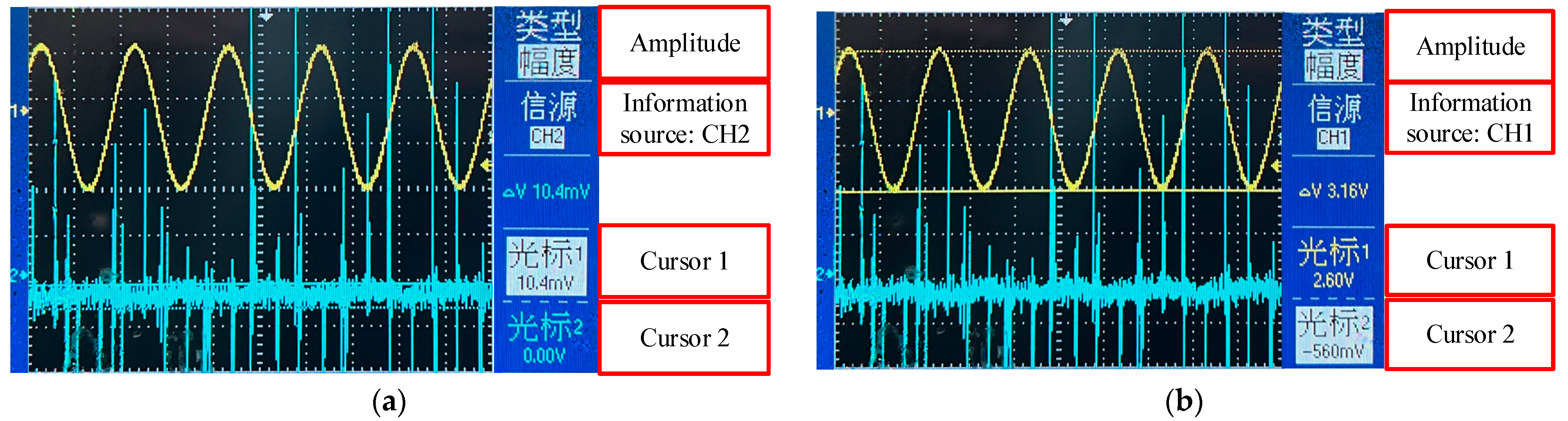
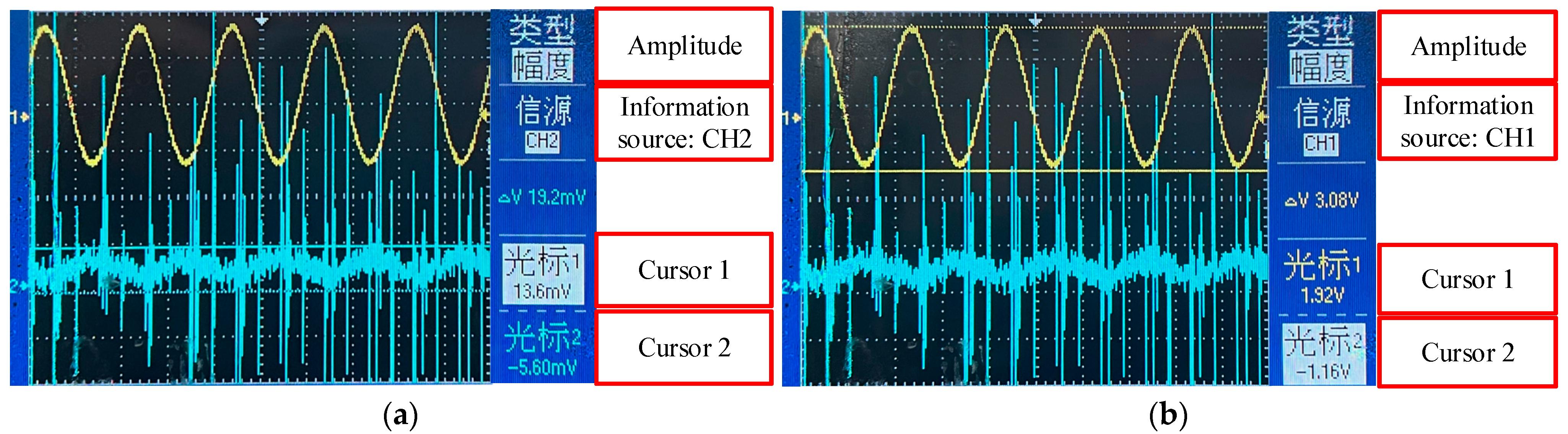
4.2.2. Induced-Signal Processing Circuit Test Experiment

In the induced-signal processing circuit test experiment, the original induction signals from the SIN+ and SIN− pins of the round inductosyn’s coarse channel and fine channel were selected and input in a differential manner. After debugging the circuit, the input/output waveforms were recorded using an oscilloscope, as shown in Figure 13 and Figure 14.
In Figure 13, CH2 is the differential signal at the SIN end of the round inductosyn’s coarse channel. According to the previous description, the amplitude of the single-ended signal at the SIN+ end of the round inductosyn is approximately 5 mVp-p; hence, the measured differential signal is 10 mVp-p, which aligns with the expected results. After passing through the signal processing circuit for amplification, filtering, and phase shifting, the output waveform is shown in CH1 of Figure 10, with an amplitude of 3.16 Vp-p. The waveform is smooth, exhibits clear sinusoidal characteristics, and has a phase shift of less than 44° compared to the excitation signal.
From CH1 in Figure 14, it can be observed that the original induced-signal output from the fine channel is approximately greater than twice that of the coarse channel. After passing through the induced-signal processing circuit, the amplitude reaches 3.08 Vp-p, which aligns with the theoretical calculations and simulation test results. The induced-signal processing circuit meets the design specifications of the circuit.

4.3. Experimental Results Analysis

In the Multisim simulation experiment, the excitation signal output from the AD2S1210 chip’s EXC+ and EXC− pins, as well as the induced signal from the coarse channel SIN+ terminal of the round inductosyn, were simulated by setting an external signal source. The output signals of each functional module were then detected. The simulation results of the decoding circuit are in line with the theoretical design results, meeting the design requirements.
In the physical experiment of the decoding circuit, the excitation signal of the dual-channel round inductosyn is directly generated by the AD2S1210. This excitation signal is input to the round inductosyn through a power amplification circuit. Waveform recordings from an oscilloscope and feedback from the induced-signal output indicate that the excitation signal effectively drives the round inductosyn’s operation. The induced signals from the coarse and fine channels, SIN+ and SIN−, are differentially inputted for testing. Although the original induced-signal amplitudes from the coarse and fine channels differ by a factor of two and exhibit significant noise, comparing the oscilloscope results after signal processing reveals that both channel signals can be amplified to meet the input requirements of the AD2S1210 and filter out noise, retaining a relatively intact sinusoidal characteristic.
The simulation and physical experiment results demonstrate that the decoding circuit meets the design requirements and can achieve the expected functionality, thereby validating the feasibility of the proposed solution presented in this paper.

5. Conclusions

This article creatively explores the use of two AD2S1210 devices in a dual-channel round inductosyn by connecting them in parallel using the same clock crystal oscillator for synchronized dual-channel decoding. Based on the input/output signal characteristics of the JGX120/360 dual-channel round inductosyn developed by Changzhou Weinengda Precision Machinery Co., Ltd., a decoding circuit is designed. The feasibility of the design scheme is verified through Multisim simulation and practical circuit testing, demonstrating the effectiveness of the design approach. Through the decoding circuit designed based on AD2S1210 in this paper, complex analog signal processing in the input/output of the dual-channel round inductosyn can be avoided. This allows for the direct digital transmission of angular position information to the system microprocessor, greatly simplifying the operational process of the dual-channel round inductosyn. In the future, we will further simplify the decoding circuit, increase system reliability and integration, use AI technology to optimize software algorithms such as noise reduction filtering and signal processing, and improve decoding accuracy based on the special requirements of a dual-channel round inductosyn applied to high-orbit satellites.

Author Contributions

Investigation, Z.H., J.W. (Jian Wang) and Y.Z.; Writing—original draft, J.W. (Jianyuan Wang); Writing—review & editing, J.W. (Jianyuan Wang); Supervision, J.C.; Funding acquisition, J.C. All authors have read and agreed to the published version of the manuscript.

Funding

This research received no external funding.

Institutional Review Board Statement

Not applicable.

Informed Consent Statement

Not applicable.

Data Availability Statement

Data is contained within the article.

Conflicts of Interest

The authors declare no conflicts of interest.

References

  1. Li, L.; Yuan, L.; Wang, L.; Zheng, R.; Wang, X.-Y.; Wu, Y.-P. Influence of micro vibration on measurement and pointing control system of high performance spacecraft from Hubble Space Telescope. Opt. Precis. Eng. 2020, 28, 2478–2487. [Google Scholar] [CrossRef]
  2. Liu, X.; Hu, W.; Ding, W.; Xu, H.; Zhang, Y. Research on Multi-Parameter Identification Method of Permanent Magnet Synchronous Motor. Trans. China Electrotech. Soc. 2020, 35, 1198–1207. [Google Scholar]
  3. Yi, Z.; Zhang, M.; Wei, H. High Precision Rotor Position Observation of Permanent Magnet Synchronous Motor Based on Hall Sensors. Trans. China Electrotech. Soc. 2019, 34, 4642–4650. [Google Scholar]
  4. Shen, Y.; Xu, Y.; Sheng, X.; Wan, S.; Yin, X. Vibration Energy Transfer Characteristics of Panels with Multiple Coupling Forms in Satellites. Int. J. Aeronaut. Space Sci. 2023, 24, 1231–1243. [Google Scholar] [CrossRef]
  5. Mu, G.; Cai, T.; Yan, G.; Liu, H.; Liu, S. Bidirectional power constraints and influence of doubly fed induction generator participating incontinuous frequency regulation. Trans. China Electrotech. Soc. 2019, 34, 3620–3630. [Google Scholar]
  6. Zhao, Y.; Han, B.; Chen, B. Speed and Rotor Position Estimation for PMSM Based on Hall Vector Phase-Tracking. Trans. China Electrotech. Soc. 2019, 34, 3147–3156. [Google Scholar]
  7. Cui, J.; Wang, X.; Xu, C. Design of high precision angle measuring system based on two speed resolver. Electron. Des. Eng. 2018, 26, 136–144. [Google Scholar]
  8. Lin, J.; Chen, W.; Xia, Z.; Hu, J. Multi-channel Induction Synchronizer's High-Precision Fusion and Implementation on FPGA. J. Astronaut. Metrol. Meas. 2021, 41, 57–62. [Google Scholar]
  9. Huo, Y.; Ren, S.; Li, W. Measurement method for sector etching error of round inductosyn. Electr. Mach. Control 2019, 23, 19–26. [Google Scholar]
  10. Liu, C.; Zhang, Y.; Sun, J. Harmonic Suppression of Output Potential of Small Size Double-RowWinding Inductosyn. Trans. China Electrotech. Soc. 2023, 38, 91–99. [Google Scholar]
  11. Wang, Y.; Bao, P.; Chen, J.; Wang, H.; Cheng, X. Design of resolver signal decoding based on FPGA. Electron. Des. Eng. 2022, 30, 75–79. [Google Scholar]
  12. Arita, S.; Yamagiwa, Y. Relationship between Magnetic Field Interference and Electromagnetic Drag in Multicoil Magnetic Sails. Int. J. Aeronaut. Space Sci. 2023, 24, 1336–1345. [Google Scholar] [CrossRef]
  13. An, S.; Bai, C.; Li, M.; Zheng, J. Design and Implementation of Angle and Position Decoding Circuit for Servo System. Aeronaut. Comput. Tech. 2020, 50, 116–119. [Google Scholar]
  14. Li, T.; Qi, X.; Xia, Z. Analysis of Influence of Induction Synchronizer Pre-Processing Analog Circuit Error on System Measurement Accuracy. J. Astronaut. Metrol. Meas. 2019, 36, 57–61. [Google Scholar]
  15. Yu, A.; Wang, C.; Guo, X.; Li, Z.; Zhang, C.; Guerrero, J.M. New Rotor Position Redundancy Decoding Method Based on Resolver Decoder. Micrimachines 2022, 13, 903. [Google Scholar] [CrossRef]
  16. Jiang, Y. Research on Absolute Inductosyn Angle Measuring System. Harbin Institute of Technology: Harbin, China, 2022. [Google Scholar]
  17. Wang, F.; Fu, J.; Han, J. Design and Realization of absolute Round Inductosyn Angle Measuring System Based on FPGA. INFRARED 2017, 18, 31–36. [Google Scholar]
  18. Han, J.; Zhang, H.; Du, Y. Research of Signal Processing Technology of Flap and Slat Angle Transducer Based on Sine and Cosine Rotating Transformer. Aeronaut. Sci. Technol. 2023, 34, 82–88. [Google Scholar]
  19. Filippo, L.; Pratticò, D.; Angiulli, G.; Oliva, G.; Pullano, S.A.; Versaci, M.; La Foresta, F. Development of an integrated System of sEMG Signal Acquisition, Processing, and Analysis with Al Technigues. Signals 2024, 5, 476–493. [Google Scholar]
  20. Fayazi, M.; Colter, Z.; Afshari, E.; Dreslinski, R. Applications of Artificial Intelligence on the odelingand Optimization for Analog and Mixed-Signal Circuits: A Review. IEEE Trans. Circuits Syst. Regul. Pap. 2021, 68, 2418–2431. [Google Scholar] [CrossRef]
  21. Rayan, M.; Jabbour, C.; Sakr, G.E. A Review of Machine Learning Techniques in Analog integrated Circuit Design Automation. Electronics 2022, 11, 435. [Google Scholar] [CrossRef]
  22. Li, M.; An, S.; Duan, Y. A position decoding and monitoring method for rotary transformers based on AD2S1210. Inf. Technol. Informatiz. 2021, 4, 139–140. [Google Scholar]
  23. Lou, M.; Zhao, Y. Research on angle measurement technology based on high-precision AD axis angle conversion chip. Technol. Innov. Appl. 2019, 28, 163–164. [Google Scholar]
  24. Song, J.; Wang, Y.; Wu, J.; Guo, Z. Research on Rotor Angle Detection of Permanent Magnet Motor Based on TMS320F28377. Electr. Mach. Control Appl. 2022, 49, 43–47+68. [Google Scholar]
Figure 1. Diagram of the dual-channel round inductosyn.
Applsci 14 09801 g001
Figure 2. Electrical schematic diagram of the dual-channel round inductosyn.
Applsci 14 09801 g002
Figure 3. Overall hardware connection diagram of the decoding circuit.
Applsci 14 09801 g003
Figure 4. Excitation signal power amplification circuit schematic.
Applsci 14 09801 g004
Figure 5. Schematic diagram of the induced-signal processing circuit.
Applsci 14 09801 g005
Figure 6. Power-amplifier circuit—Multisim simulation circuit.
Applsci 14 09801 g006
Figure 7. Excitation-signal power-amplifier circuit—Multisim simulation waveform.
Applsci 14 09801 g007
Figure 8. Induced-signal processing circuit—Multisim simulation circuit.
Applsci 14 09801 g008
Figure 9. Induced-signal processing circuit—Multisim simulation waveform.
Applsci 14 09801 g009
Figure 10. Induced-signal amplification and filtering circuit phase–frequency characteristics curve.
Applsci 14 09801 g010
Figure 11. Round inductosyn decoding-circuit experimental testing platform: (a) excitation-signal input; (b) AD2S1210 excitation-signal power-amplification circuit; (c) oscilloscope results.
Applsci 14 09801 g011
Figure 12. Waveforms before and after the amplification of the excitation signal (CH1 is the signal after the amplification of excitation, and CH2 is the signal before the amplification of excitation).
Applsci 14 09801 g012
Figure 13. Coarse-channel SIN-induced signal processing result (CH1 is the output signal, and CH2 is the input signal): (a) input signal amplitude; (b) output signal amplitude.
Applsci 14 09801 g013
Figure 14. Fine-channel SIN-induced signal processing result (CH1 is the output signal, and CH2 is the input signal): (a) input signal amplitude; (b) output signal amplitude.
Applsci 14 09801 g014
Table 1. Decoding-circuit design specifications.
Signal TypeDesign Specifications
Excitation Signal Amplitude7.2 Vp-p ± 1.0 V
Induced signal amplitude(single-ended)1.6 Vp-p ± 0.3 V
Induced Signal Amplitude (Differential)3.2 Vp-p ± 0.6 V
Amplitude Difference between the SIN and COS Terminals<0.1 V
Phase Difference between the SIN and COS Terminals<5.0°
Phase Difference between Induced and Excitation Signal<44.0°
Table 2. The signals and amplitudes corresponding to each channel in Figure 7.
ChannelSignal TypeAmplitude
CH1SIN+ Original Induced Signal4.8 mVp-p
CH2Amplifier Output Signal1.5 Vp-p
CH3Filtered Output Signal1.6 Vp-p
CH4Phase-shifted Output Signal1.6 Vp-p
Disclaimer/Publisher’s Note: The statements, opinions and data contained in all publications are solely those of the individual author(s) and contributor(s) and not of MDPI and/or the editor(s). MDPI and/or the editor(s) disclaim responsibility for any injury to people or property resulting from any ideas, methods, instructions or products referred to in the content.

