Article

Interleaved Modified SEPIC Converters with Soft Switching and High Power Factor for LED Lighting Appliance

Department of Electrical Engineering, I-Shou University, Kaohsiung City 84001, Taiwan
*
Author to whom correspondence should be addressed.
Appl. Sci. 2024, 14(15), 6656; https://doi.org/10.3390/app14156656
Submission received: 28 May 2024 / Revised: 22 July 2024 / Accepted: 25 July 2024 / Published: 30 July 2024
(This article belongs to the Section Optics and Lasers)

Abstract

:
A novel ac/dc LED driver with power factor correction and soft-switching functions is proposed. The circuit topology mainly consists of two modified single-ended primary inductance converters (SEPIC) with interleaved operation. The first half stage of SEPIC operates like a boost converter and the second half stage operates like a buck–boost converter. Each boost converter is designed to operate in discontinuous current mode (DCM) to function as a power factor corrector (PFC). The two buck–boost converters that share a commonly coupled inductor are designed to operate at near boundary conduction mode (BCM). Without using any active clamping circuit, auxiliary switch or snubber circuit, the active switches can achieve zero-voltage switching on, and all diodes achieve zero-current switching off. First, operation modes in steady state are analyzed, and the mathematical equations for design component parameters are derived. Finally, a prototype circuit of 180 W rated power was built and tested. Experimental results show satisfactory performance of the proposed circuit.

1. Introduction

A light-emitting diode (LED) has the advantages of small size, high energy efficiency, long service life, fast response time, good color rendering, environmental friendliness, etc. Nowadays, LEDs have gradually replaced fluorescent lamps and high-intensity gas discharge lamps, and have been widely used in various lighting systems [1,2,3,4].
When the input voltage is an ac line voltage source, a large capacitor filter needs to be installed after the rectifier circuit to reduce the ripple of the rectified dc voltage. Since the diode of the rectifier circuit only conducts when the ac voltage is higher than the dc voltage. The conduction time is very short, and the input current is a large pulse inrush current. This results in a low power factor and high total harmonic distortion of current (THDi) [5]. High-order harmonic currents can interfere with control circuits or communication systems and cause malfunctions in measuring instruments and electrical protection equipment. Therefore, advanced countries have formulated strict specifications, such as IEC 61000-3-2 [6] and IEEE 519 [7] to regulate the power factor and THDi of electrical products [8,9]. In order to meet the specifications of power factor and THDi, a power factor corrector (PFC) should be added in front of the original ac/dc converter, so that the LED drivers have a two-stage circuit architecture [10,11]. In order to improve the shortcomings of using more components in a two-stage converter and to reduce the number of energy transfer times in the converter and thereby improve the circuit efficiency, researchers have developed a number of single-stage LED drivers in which the active switches and control circuit are shared by a PFC converter and a dc/dc converter [12,13,14,15,16,17]. However, in order to serve as switches for both the PFC converter and the DC/DC converter, some shared switches operate in hard switching.
Hard switching means that the switch cannot operate at zero-voltage switching on (ZVS) or zero-current switching off (ZCS). For active switches, if they cannot operate at ZVS, their parasitic capacitance will generate huge spike currents due to an instant short circuit when they are turned on, and the energy originally stored in the parasitic capacitance will be dissipated inside the switches. For diodes, if they cannot operate at ZCS, a reverse recovery current will be generated when the diodes are turned off. In other words, in addition to huge switching losses, hard switching is also accompanied by high current and high voltage stress. Therefore, hard switching circuits must use switches with high voltage/current specifications to reduce their failure rate. Without the use of higher specification components, the LED drivers with hard switching can only be used in low-power products. The literature [18,19,20] proposed LED drivers with single-stage topologies. Although they can achieve a high power factor, their energy conversion efficiency is not high because the active switches cannot meet ZVS operation, so they are only suitable for low-power products (9–50 W). In order to solve the hard-switching problem, pulse–width modulation (PWM) converters usually use active clamping or snubber circuits to implement ZVS and/or ZCS [21,22,23,24]. However, these soft-switching techniques require the use of additional auxiliary switches, diodes, inductors, and capacitors, which increases circuit costs. In addition, current loops in active clamping or snubber circuits generate additional conduction losses, thereby reducing circuit efficiency. In the literature [25,26,27,28], a single-stage topology is obtained by integrating a PWM converter and a resonant converter, where the PWM converter is used as the PFC circuit and the full-bridge or half-bridge resonant converter is used as the DC/DC converter. The resonant converter not only has the advantage of galvanic isolation. By designing the switching frequency to be greater than the resonant frequency of the resonant tank, the resonant tank will present an inductive load, and the active switches can operate at ZVS. However, the resonant converter requires additional rectifier and filter circuits to obtain a smooth DC output voltage, which not only increases the component count but also causes more conduction losses.
This paper proposes an ac/dc converter to drive high-power LEDs, which is obtained by modifying two single-ended primary inductance converters (SEPIC) with interleaved operation. The proposed circuit achieves a high power factor and low THDi and the switch meets soft switching. The other content of this paper is organized as follows. Section 2 proposes the circuit topology and analyzes the steady-state operation mode in detail; Section 3 deduces the mathematical equations for designing circuit component parameters; Section 4 designs, manufactures and experimentally measures the 180 W prototype circuit. Finally, some conclusions are made in Section 5.

2. Proposed LED Driver and Analysis of Steady-State Operation

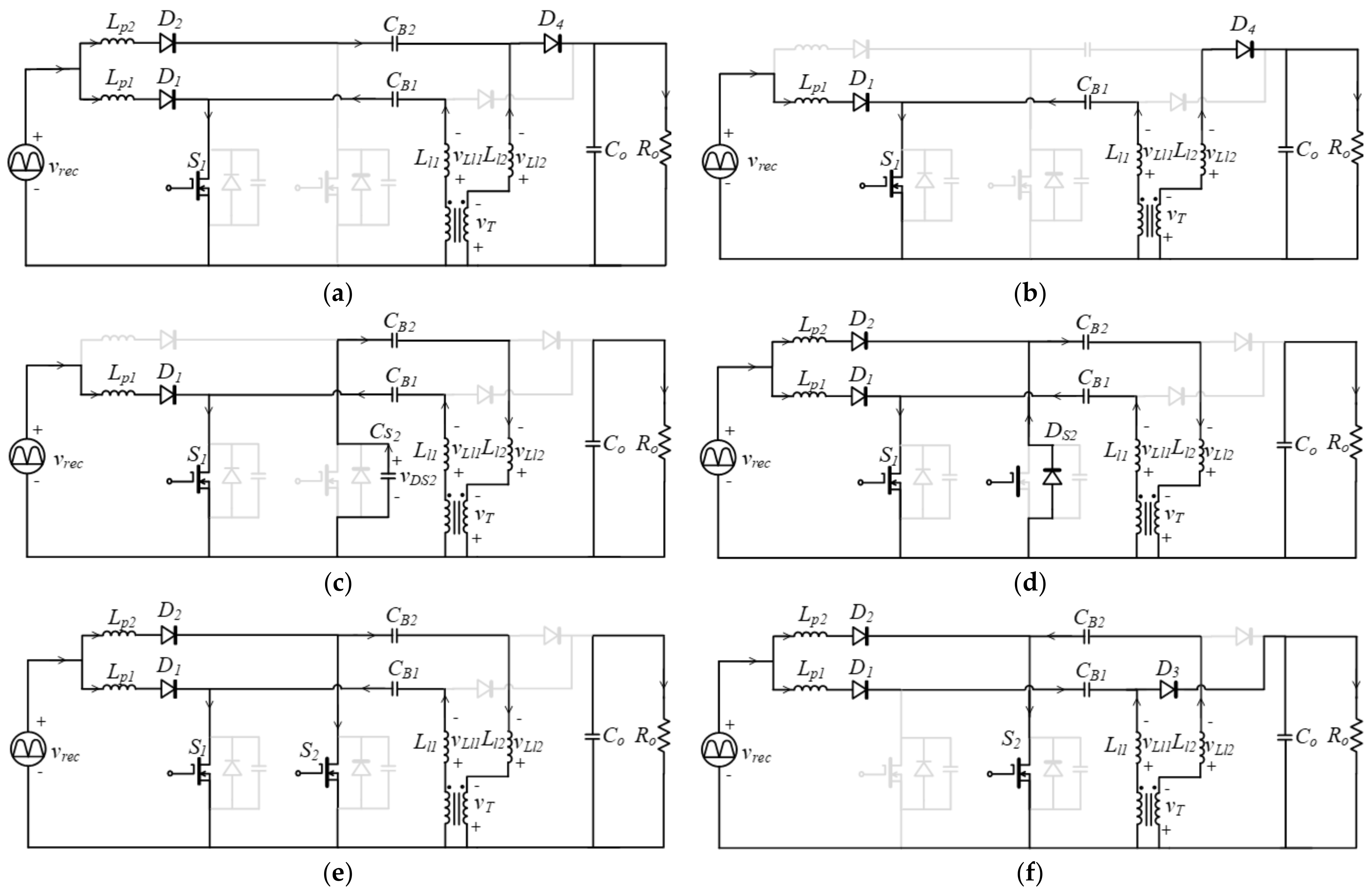
2.1. Circuit Topology

Figure 1 shows the circuit topology of the high-power factor ac/dc LED driver proposed in this paper. The circuit consists of a low-pass filter (Lf, Cf), a bridge rectifier (Dr1Dr4), and two modified SEPIC circuits. One SEPIC circuit includes inductor Lp1, diode D1, active switch S1, dc-link capacitor CB1, flywheel diode D3 and the primary winding of the coupled inductor T1, and the other includes inductor Lp2, diode D2, active switch S2, dc-link capacitor CB2, flywheel diode D4 and secondary winding of T1. Diodes DS1 and DS2 are the intrinsic body diodes of S1 and S2, respectively. Figure 2 shows the control voltages (vGS1, vGS2) of S1 and S2. They are both square wave voltages with a phase difference of 180 degrees and partially overlap, i.e., both S1 and S2 are in conduction for a certain period of time.
Typically, a SEPIC circuit is a single-stage topology using only one active switch. The first half stage of the SEPIC circuit operates like a boost converter and the second half operates like a buck–boost converter. Compared with the traditional two parallel SEPIC circuits, the circuit proposed in this paper has two differences. The first is the addition of two diodes (D1, D2) to avoid the currents in Lp1 and Lp2 flowing in the opposite direction. If ip1 and ip2 have reverse currents, the power factor correction performance will be impaired, and some excess conduction loss will occur. The second point is to use a coupled inductor T1 instead of two separate inductors for the second half stage of the two SEPIC circuits. T1 consists of an iron core and two windings with the same number of turns. Unlike traditional SEPIC circuits, which require additional components to enable ZVS operation for active switches. The winding current of the coupled inductor is designed to operate close to the boundary conduction mode (BCM). Based on the principle of magnetomotive force balance, the mutual inductance current will be converted between the two windings and the winding current is used to discharge the store charges in the parasitic capacitance of the active switch to fulfill ZVS operation.

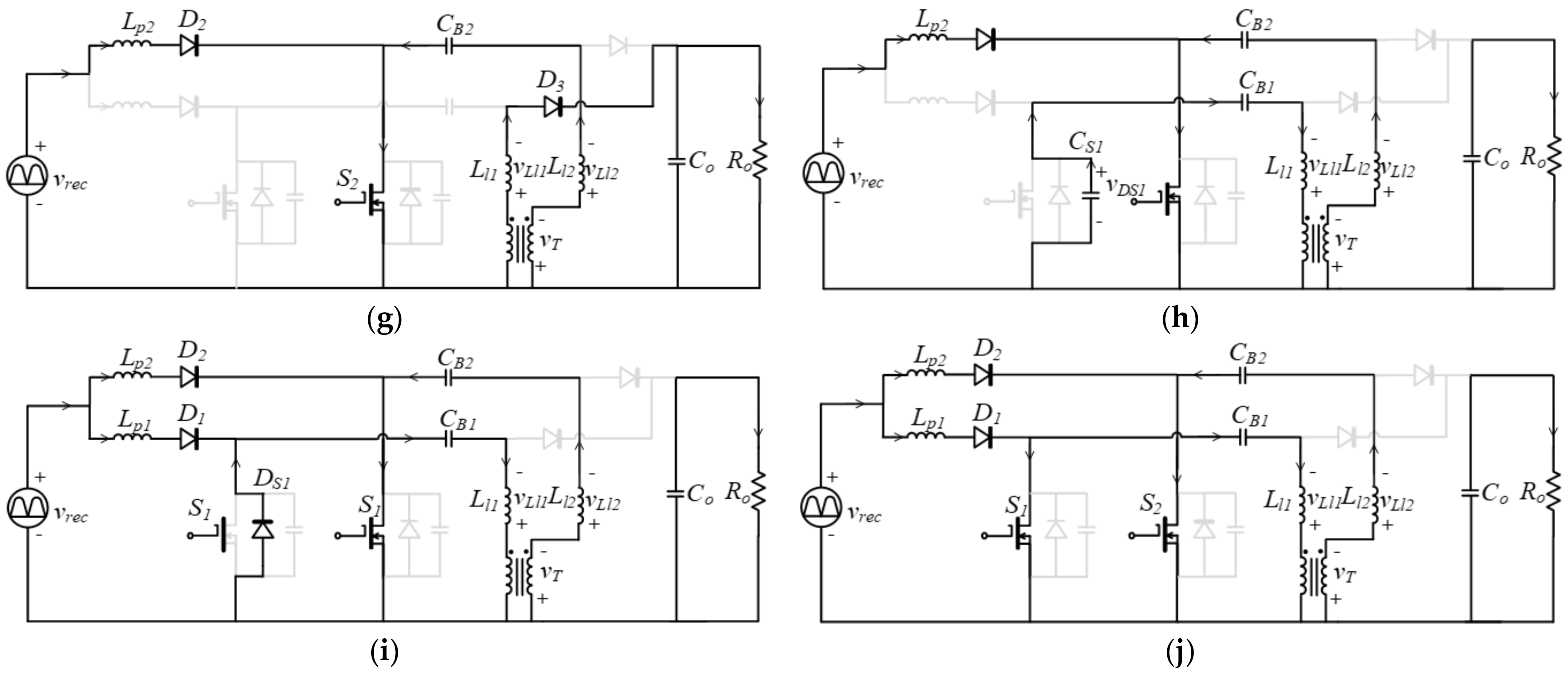
2.2. Analysis of Operation Mode

The following assumptions are made to simplify the circuit analysis.
(1)
In order to ensure ZCS operation for all diodes, the currents of Lp1 and Lp2 are designed to operate in discontinuous-current mode (DCM), and the winding currents of T1 are all designed to decrease to zero amps.
(2)
All components are considered ideal except for the parasitic capacitance (CS1 and CS2) and intrinsic diodes (DS1 and DS2) of the S1 and S2.
(3)
The two SCPIC circuits are identical with Lp1 = Lp2 = Lp, CB1 = CB2 = CB, VB1 = VB2 = VB.
(4)
Capacitors CB1, CB2, and Co are large enough that the voltages across them (VB1, VB2, and VO) can be regarded as constant.
(5)
The winding resistance and iron loss of T1 are neglected. The leakage inductance in the primary and secondary windings are equal (Ll1 = Ll2 = Ll), and the mutual inductance Lm is large enough so that the mutual inductance current is regarded as a constant ILm.
(6)
S1 and S2 are turned on and off at a high frequency (fs) well above the input line frequency (fL). Therefore, the rectified input voltage can be regarded as a constant value in each high-frequency cycle.
In steady-state operation, the circuit can be divided into 10 operation modes in each high-frequency cycle according to the status of each component. Figure 3 shows the equivalent circuits for each operation mode, where vrec denotes the voltage after the bridge rectification and Ro denotes the equivalent resistance of the LEDs. In Figure 3, T1 is represented by a transformer model, where Ll1 and Ll2 are leakage inductances and vT is the voltage across the mutual inductance. For a coupled inductor, the following equation can be derived [29].
i L l 1 + i L l 2 = i L m ,
v T = L m d i L m d t ,
Applying Faraday’s law to the leakage inductances gives
v L l 1 + v L l 2 = L l 1 d i L l 1 d t + L l 2 d i L l 2 d t = L l d i L m d t ,
Figure 4 shows the schematic waveforms of voltage and current of the main components. The following section describes the details of each operation mode and the derivation of the associated equations.
Before operation Mode 1, both S1 and S2 are on. Since S2 is turned on before S1, most of the mutual inductance current iLm flows in the secondary winding of T1 through S2, that is, iLl2 >> iLl1. When vGS2 changes from high level to low level, S2 is turned off and the circuit enters operation Mode 1.

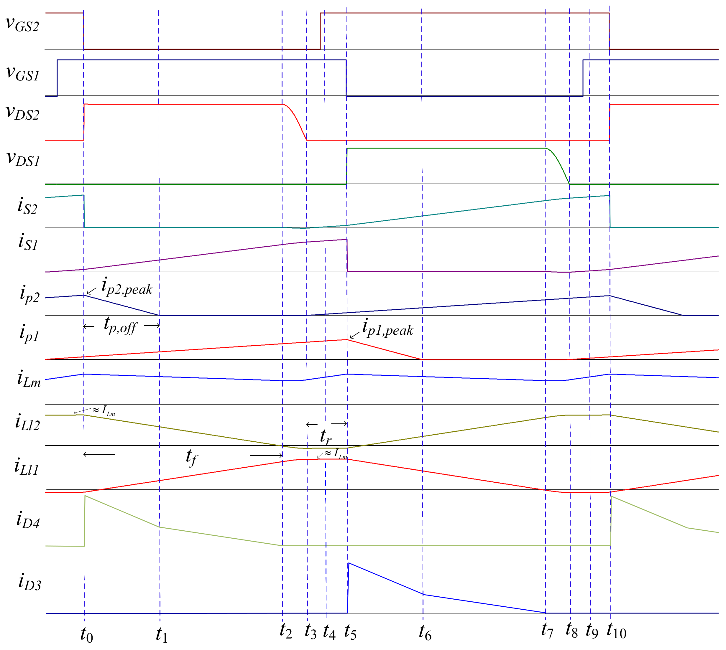
2.2.1. Operation Mode 1 (t0 < t < t1)

At the moment before S2 is turned off, ip2 reaches a peak value, denoted as ip2,peak. When S2 is turned off, ip2 flows through D2 to charge CS2, and iLl2 also flows into CB2 to charge CS2. In practice, the parasitic capacitance is very small. CS2 will be quickly charged to VB + Vo. After that, ip2 will flow through D2, CB2, D4, and Co, while iLl2 will flow through D4 and Co, as shown in Figure 3a. The voltages and current equations for Lp1 and Lp2 are as follows.
v p 1 t = v r e c ,
i p 1 t = i p 1 t 0 + v r e c L p t t 0 ,
v p 2 t = V B V o + v r e c ,
i p 2 t = i p 2 , p e a k V B + V o v r e c L p t t 0 ,
The current ip1 keeps increasing linearly while ip2 starts to decrease linearly.
From Figure 3a, the voltage equations of the primary and secondary windings of T1 are expressed as (8) and (9), respectively.
v L l 1 + v T = V B ,
v L l 2 + v T + V o = 0 ,
Adding (8) and (9) gives
v L l 1 + v L l 2 + 2 v T = V B V o ,
Substituting (2) and (3) into (10) yields
v T = L m L l + 2 L m V B V o ,
Substituting (11) into (8) and (9), respectively, the leakage inductance voltages can be expressed as follows.
v L l 1 = L m + L l V B + L m V o L l + 2 L m ,
v L l 2 = L m V B L m + L l V o L l + 2 L m ,
Equation (12) shows that vLl1 is positive, so iLl1 starts to rise from a negative value close to zero. After a period of time, iLl1 rises to become positive. Equation (13) shows that vLl2 is negative, and iLl2 starts to decrease from the peak value. In other words, when S2 is turned off, iLl2 decreases and iLl1 increases, that is, the current originally flowing through the secondary winding of T1 gradually converts to flow through the primary winding.
The boost converters would be designed to operate in DCM. When ip2 declines to zero, D2 turns off and the circuit enters the next operation mode.

2.2.2. Operation Mode 2 (t1 < t < t2)

In this mode, the equivalent circuit is shown in Figure 3b. The current ip2 remains zero. Equations (4), (5), and (8)–(13) remain unchanged. Therefore, ip1 and iLl1 continue to rise, and iLl2 continues to fall. When iLl2 decreases to zero, D4 turns off and the circuit enters the next operation mode.

2.2.3. Operation Mode 3 (t2 < t < t3)

In this mode, ip2 remains zero while ip1 keeps increasing. This mode is the process of discharging CS2 from high voltage to zero volts. As shown in Figure 3c, vLl1 and vLl2 can be expressed as follows.
v L l 1 = V B v T ,
v L l 2 = V B v T v D S 2 ,
Adding (14) and (15) gives
v L l 1 + v L l 2 = 2 V B 2 v T v D S 2 ,
Substituting (2) and (3) into (16) yields
v T = L m L l + 2 L m 2 V B v D S 2 ,
Substituting (17) into (14) and (15) respectively, vLl1 and vLl2 can be expressed as follows.
v L l 1 = L l V B + L m v D S 2 L l + 2 L m ,
v L l 2 = L l V B L m + L l v D S 2 L l + 2 L m ,
At the beginning of this mode, vDS2 is equal to VB + Vo, (18) and (19) show that vLl1 is positive, and vLl2 is negative. The current iLl1 keeps on rising. On the contrary, iLl2 continues to decrease and becomes negative, i.e., the secondary winding current is reversed, and at this time, T1 acts as a transformer. During the discharge of CS2, vDS2 decreases. Observing (17)–(19), it can be known that vT and vLl2 increase, and vLl1 decreases. When CS2 discharges to zero volts, DS2 turns on and the circuit enters operation Mode 4.

2.2.4. Operation Mode 4 (t3 < t < t4)

Figure 3d shows the equivalent circuit of operation Mode 4. The voltage and current equations of Lp2 are
v p 2 t = v r e c ,
i p 2 t = v r e c L p t t 3 ,
The current ip2 starts to rise from zero. The voltage equations of the primary and secondary windings of T1 are
v L l 1 + v T = V B ,
v L l 2 + v T = V B ,
Adding (22) and (23) gives
v L l 1 + v L l 2 + 2 v T = 2 V B ,
Substituting (2) and (3) into (24) yields
v T = 2 L m L l + 2 L m V B ,
Substituting (25) into (22) and (23), respectively, vLl1 and vLl2 can be expressed as follows.
v L l 1 = v L l 2 = L l L l + 2 L m V B ,
Equations (25) and (26) show that vT is positive, and vLl1 and vLl2 are also positive and equal, therefore, iLm, iLl1 and iLl2 all rise. Because Lm is much larger than Ll, (26) shows that vLl1 and vLl2 are very small, therefore, iLl1 and iLl2 rise slowly.
Observing Figure 3d, it can be noticed that iLl2 has two current paths, one is CB2T1 secondary winding–DS2, and the other is CB2T1 secondary winding–vrecLp2D2. Before iLl2 rises from negative to zero, vGS2 changes from low level to high level. Because iLl2 is negative, its absolute value becomes smaller during the rise process. At first, the absolute value of is iLl2 larger than ip2. When ip2 rises to become larger than the absolute value of iLl2, S2 would be turned on and the circuit enters operation Mode 5.

2.2.5. Operation Mode 5 (t4 < t < t5)

Figure 3e shows the equivalent circuit of this mode. Because DS2 is in the on-state before S2 is turned on, it clamps vDS2 at zero volts, therefore S2 satisfies ZVS. In this mode, ip2 has two current loops, which are Lp2D2CB2T1 secondary winding–vrec, and Lp2D2S2vrec. DS2 is on when the circuit is operating in mode 4 and S2 is on when the circuit is operating in mode 5. Whether DS2 is on or S2 is on, vDS2 is equal to zero volts, so the voltage and current equations for Mode 5 are identical to Mode 4. Hence, ip1 and ip2 all continue to rise. When vGS1 changes from high level to low level, S1 is turned off and the circuit enters operation Mode 6.

2.2.6. Operation Mode 6 (t5 < t < t6) ~ Operation Mode 10 (t9 < t < t10)

Figure 3f–j show the equivalent circuits of Mode 6 to Mode 10. The circuit operation principles of Mode 6 to Mode 10 are similar to those of Mode 1 to Mode 5 and will not be described again here. When vGS2 changes from high level to low level, S2 is turned off, and the circuit enters the next high-frequency cycle of operation Mode 1.

3. Mathematical Equations for Parameters Design

3.1. Boost-Typed PFC Converter

From the analysis of the operation mode, it can be known that the voltage across Lp1 (Lp2) is equal to vrec when S1 (S2) is on. On the contrary, when S1 (S2) is turned off, Lp1 (Lp2) transfers the stored energy to CB1 (CB2) and Co. Lp1 (Lp2) is served as the inductor of a boost converter. In order for the boost converter to operate in DCM throughout the input voltage cycle, VB +Vo must be high enough to satisfy the following equation.
V B + V o V m 1 D ,
First, k is defined as
k V B + V o / V m ,
When the value of k is greater than 2, the power factor can reach more than 0.98 and the output power can be expressed as [30]
P o = η D 2 V m 2 L p f s y ,
where η represents the circuit efficiency and y is expressed as
y = 0 π sin 2 θ 1 1 k sin θ   d θ = k 3 k 2 1 1 + 2 π sin 1 1 k k 2 2 π k ,

3.2. Buck–Boost Converter

Based on the previous assumptions, iLm can be regarded as a constant value ILm when Lm is sufficiently large. During Mode 1 and Mode 2, iLl1 rises and iLl2 decreases, and it is known that the increase in iLl1 is equal to the decrease in iLl2 by (1). Mode 3 describes the process in which the parasitic capacitance of S2 is discharged from VB + Vo to zero volts. Because CS2 is very small and the drop in iLl2 is also very small, therefore, at the end of Mode 3, iLl2 is negative but almost equal to zero. Thus, it is known that the peaks of iLl1 and iLl2 are very close to ILm.
i L l 1 , p e a k = i L l 2 , p e a k I L m ,
Operation Mode 2 ends when iLl2 decreases to zero. Using (13) and (31), the time required for iLl2 to decrease from the peak value to zero is equal to
t f = t 2 t 0 I L m L l L l + 2 L m L m V B + L m + L l V o ,
During the period from Mode 1 to Mode 2, vT is negative and iLm decreases. On the contrary, during the period from Mode 3 to Mode 5, vT is positive and iLm increases. Applying the volt–second balance law of inductance, the average value of vT is equal to zero. From (11) and (25), we can obtain
v T ¯ = L m V B V o L l + 2 L m t f + 2 L m V B L l + 2 L m t r = 0 ,
where tr represents the rising time of iLm. Ignoring the short charging and discharging time of CS1 (CS2), we can obtain
t f + t r 0.5 T s ,
Combining (33) and (34), it can be deduced that tf and tr are, respectively, expressed as
t f = V B V B + V o T s ,
t r = 0.5 V B V B + V o T s ,
Because both tr and tf must be positive values, it can be seen from (36) that the design constraint for realizing the converter proposed in this study is that
V o > V B ,
Substituting (35) into (32) yields
I L m = V B L m V B + L m + L l V o L l L l + 2 L m V B + V o T s ,
From the analysis of the operation modes, it can be seen that the output power comes from two paths. One is that Lp1 (Lp2) directly provides energy to the output terminal through D3 (D4). The other is that Lp1 (Lp2) first charges CB1 (CB2) through D3 (D4), and then CB1 (CB2) provides energy to the output terminal. The power supplied to the output terminal by each of these two paths is equal to
P 1 = P o V o V B + V o ,
P 2 = P o V B V B + V o ,
For a buck–boost converter, when the active switch is turned off, the inductor current flows through the flywheel diode and releases energy to the output. Combining (35) and (38) yields that the average of the descending portions of iL1 and iL2 added together is equal to
i L l 1 ,   f a l l ¯ + i L l 2 ,   f a l l ¯ = 2 × t f I L m 2 T s = V B 2 L m V B + L m + L l V o L l L l + 2 L m V B + V o 2 f s ,
Equation (41) represents the average current delivered to the output by the buck–boost converters. Combining (40) and (41) yields
V B L m V B + L m + L l V o L l L l + 2 L m V B + V o f s = P o V o ,
The coupling coefficient of the coupled inductor is defined as
k c L m L l + L m ,
Combining (42) and (43) yields
L l = V B V o k c V B + V o 1 + k c V B + V o P o f s ,

4. Parameters Design and Experimental Results

A 180 W prototype LED driver was built and tested to demonstrate the feasibility of the proposed circuit. The specification of the proposed LED driver is listed in Table 1. The input supply voltage presented in the article is 110 Vrms ± 10%, not universal voltage (85–264 Vrms). Equation (45) shows the design constraint for the dc-link voltage and the output voltage. The higher the input voltage, the higher the dc-link voltage and the output voltage should be. Compared with other loads, the voltage of each LED is very small. High output voltage means a considerable number of LEDs per string. When there are too many LEDs per string, the design range of the output-rated power will be limited. The load consists of three LED strings connected in parallel, each string consisting of sixty 1 W LEDs. The rated voltage and current of each LED are 3.6 V and 0.28 A, respectively.

4.1. Parameters Design

The considerations and calculations of component parameters are as follows.
A.
Choose duty ratio and dc-link voltage.
As shown in Figure 2, the gate–source voltages of S1 and S2 should briefly overlap when they are at high levels, that is, the duty cycle is slightly higher than 0.5. However, a high-duty cycle requires a higher dc-link voltage for the PFC converter to operate in DCM. Here, the duty ratio is chosen to be 0.54.
D = 0 . 54
The design constraint for dc-link voltage can be obtained by combining (27) and (37), as follows.
V o > V B > V m 1 D V o ,
Considering the 10% variation in the input voltage, the applicable range of the dc-link voltage is calculated as
216 > V B > 110 2 × 1.1 1 0.54 216 = 156   V
Here, the dc-link voltage is chosen to be
V B = 1 60   V
B.
Calculate PFC inductance.
First, calculate the value of k and the value of y using (28) and (30) in sequence.
k = 160 + 216 110 × 2 = 2.42
y = 2 . 42 3 2 . 42 2 1 1 + 2 π sin 1 1 2 . 42 2 . 42 2 2 π × 2 . 42 = 0 . 78
Assuming a circuit efficiency of 95%, the PFC inductance can be calculated by using (29).
L p = 0 . 95 × 0 . 54 2 × 110 × 2 2 180 × 50 × 10 3 × 0 . 78 = 0 . 58   mH
C.
Determine the leakage inductance and the mutual inductance of T1.
Selecting a coupling coefficient of 0.9, the leakage inductance can be calculated by using (44).
L l = 0 . 95 × 160 × 216 × 0 . 9 × 160 + 216 1 + 0 . 9 × 160 + 216 × 180 × 50 × 10 3 = 1 . 84 mH
Then, the mutual inductance is calculated to be
L m = 16 . 54 mH

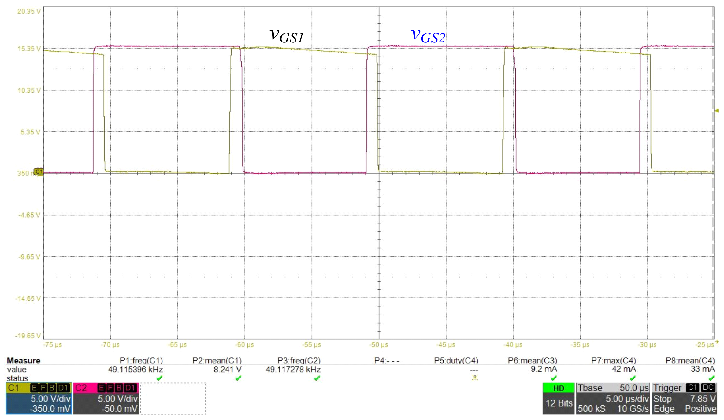
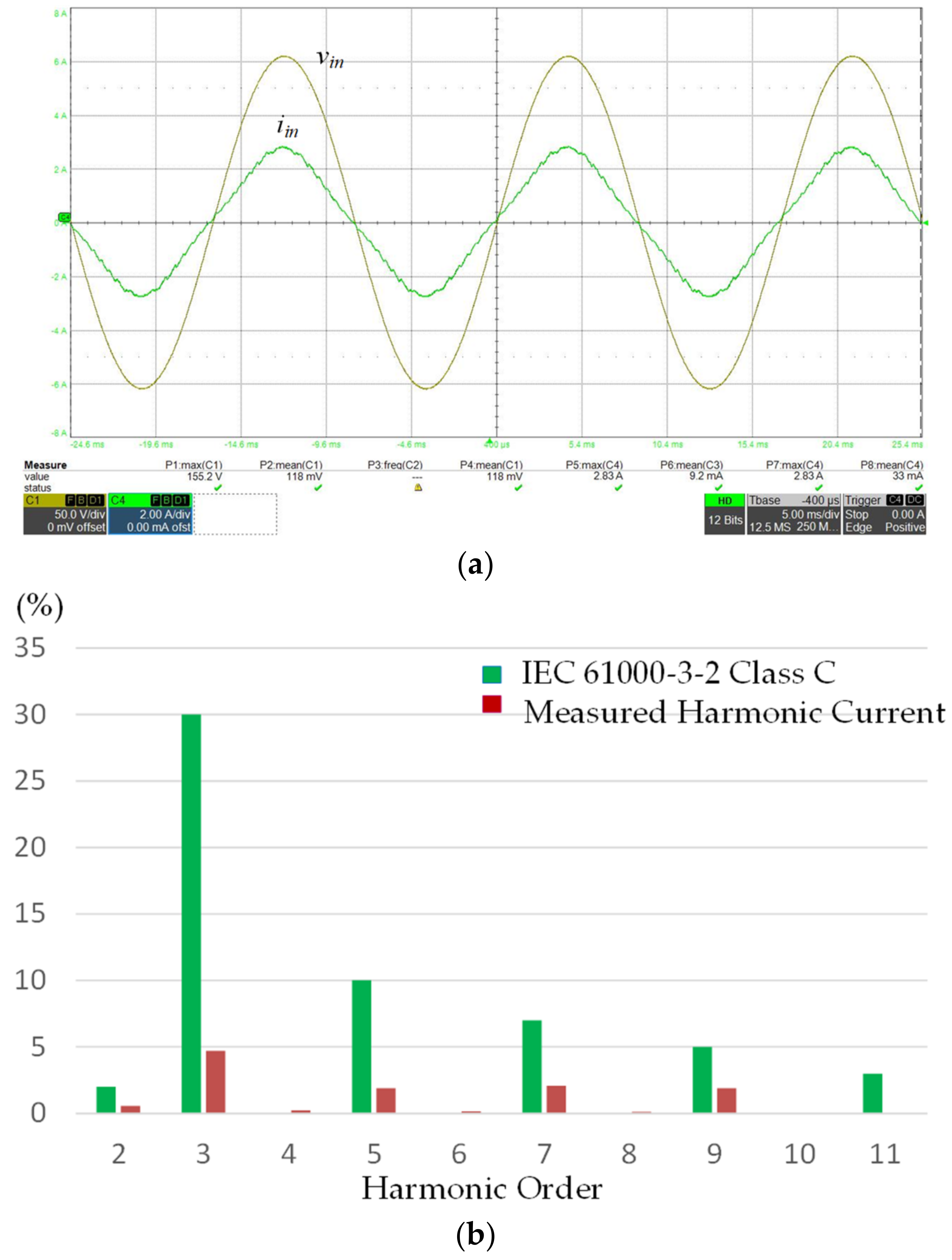
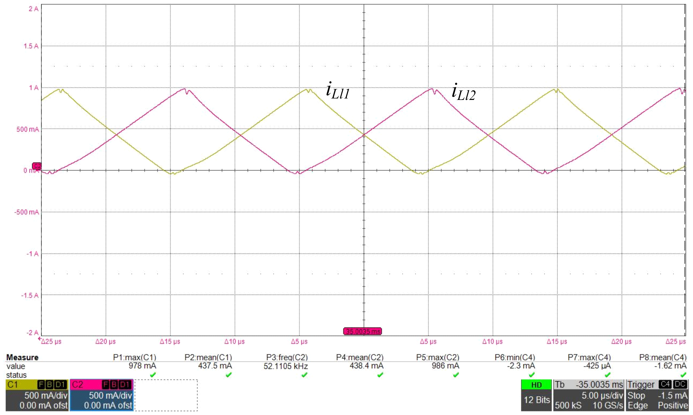
4.2. Experimental Results

Table 2 shows the component parameters of the prototype LED driver. In practice, it is not easy to produce a coupled inductor whose mutual inductance and leakage inductance meet the design values at the same time. Therefore, in this prototype circuit, first, a coupled inductor with a mutual inductance equal to 16.54 mH was implemented, and then two small inductors were, respectively, connected in series with the two windings of this coupled inductor. In addition, the sum of the leakage inductance of the coupled inductor and the inductance of each small inductor is equal to 1.84 mH.
Figure 5 shows the control voltages of the two active switches. As shown in the figure, the duty cycles of vGS1 and vGS2 both exceed 0.5, so both S1 and S2 are in a conductive state for a certain period of time. Figure 6a shows the inductor current waveforms of two PFC converters for several input voltage cycles. It can be seen that the envelope of the inductor current follows the input voltage to be a sinusoidal waveform. The peak value of the inductor current is high at high input voltage, and vice versa. Therefore, the time required for the inductor current to decrease from a peak value to zero is not the same. When the input voltage is at a high point, it requires more time for the inductor current to decrease from a peak value to zero. It can be concluded that if PFC converters can operate in DCM when the input voltage is at its peak point, then they can operate in DCM throughout the input voltage cycle. Figure 6b shows the expanded waveforms when the input voltage is near the peak value. As shown, the inductor current does decrease to zero. Figure 7a shows the waveforms of input voltage and input current. It can be seen that the input current follows the input voltage and is in phase with the input voltage. A power analyzer was used to measure the power quality of the input line. At rated power operation, the values of the active power, reactive power, and apparent power were 196.7 W, 34.5 Var, and 199.7 VA, respectively. The measured power factor and THDi are 0.985 and 5.27%, respectively. The specifications of the proposed LED were measured. Figure 7b shows the harmonic spectrum of the input current. The current harmonics are compared with the IEC 61000-3-2 Class C standard [6]. It can be seen that all measured current harmonics are below the standard. It verifies that operating a boost converter in DCM can indeed achieve a high power factor and low THDi. Figure 8 shows the current waveforms in the two windings of the coupled inductor. As mentioned in the section on analysis of operation mode, Mode 3 is the time to discharge the parasitic capacitance from high voltage to zero volts, and Mode 4 is the time for the inductor current to rise from zero to greater than the absolute value of the inductor current. Generally, the parasitic capacitance is very small. The typical output parasitic capacitance of the active switch (IPW65R080CFD, Infineon Technologies, Neubiberg, Germany) is 215 pF. Therefore, the time required for Mode 3 and Mode 4 is very short. The mutual inductance current is converted between the primary and secondary windings. When the current in one winding decreases, the current in the other winding increases. Additionally, the winding current will drop to a negative value. Although this negative current is very small, it is enough to release the parasitic capacitance of the MOSFET and allow the active switch to meet ZVS. Figure 9 shows the voltage and current waveforms of the two active switches. It can be seen from these experimental waveforms that before vGS1 (vGS2) changes from low to high level, there is a negative current that discharges the parasitic capacitance of the active switch to zero volts. This allows the active switches to be turned on at zero voltage and zero current. Figure 10 shows the LED voltage and current waveforms. The measured LED power is 181 W, which is quite close to the design target values. The circuit efficiency is 92%. In addition, it can be seen that the LED voltage exhibits low-frequency ripples (120 Hz), and the ripple factor is calculated to be approximately equal to 7%. This ripple voltage can be reduced by using larger output capacitance or larger dc-link capacitance. Figure 11 shows the photo of the proposed LED driver test stand.

5. Conclusions

This paper proposes a new LED driver with a high power factor and low total current harmonic distortion. The circuit architecture consists of two modified SEPICs that share a coupled inductor with two windings. The two SEPICs are interleaved operated, and their active switches have a duty cycle greater than 0.5. In this paper, mathematical equations are derived, and component parameters are designed so that all inductor currents would decrease to zero, allowing all diodes to operate at ZCS. In addition, the winding current of the coupled inductor can completely release the charge of the parasitic capacitance of the active switch, so that the active switch operates at ZVS, which significantly reduces the switching loss. A prototype circuit with a rated power of 180 W is implemented and measured experimentally. The experimental results show that the power factor and THDi are equal to 0.985 and 5.27%, respectively, at rated power operation. The measured efficiency of the circuit is 92%. The experimental results have verified the feasibility of the proposed circuit.

Author Contributions

H.-L.C. conceived the novel circuit topology and wrote the paper. C.-A.C. revised the original circuit and analyzed the circuit operation; C.-H.C. and E.-C.C. derived the mathematical equations and designed the circuit component. and designed parameters of the circuit components; Y.-C.H. carried out the prototype LED driver and measured as well as analyzed experimental results; L.-C.H. performed circuit simulations and revised the manuscript for submission. All authors have read and agreed to the published version of the manuscript.

Funding

This research received no external funding.

Institutional Review Board Statement

Not applicable.

Informed Consent Statement

Not applicable.

Data Availability Statement

The original contributions presented in the study are included in the article, further inquiries can be directed to the corresponding author.

Acknowledgments

This work was supported by the National Science and Technology Council, R.O.C. under Grant NSTC 112-2221-E-214-006.

Conflicts of Interest

The authors declare no conflicts of interest.

References

  1. Zhan, X.; Chung, H.; Zhang, R. Investigation into the use of single inductor for driving multiple series-connected LED channels. IEEE Trans. Power Electron. 2017, 32, 3034–3050. [Google Scholar] [CrossRef]
  2. Cheng, C.A.; Lee, C.M.; Chang, E.H.; Hou, S.H.; Lan, L.F.; Lin, C.K. A novel integrated electronic lighting driver circuit for supplying an LED projection lamp with high power factor and soft switching characteristics. Electronics 2023, 12, 4642. [Google Scholar] [CrossRef]
  3. Esteki, M.; Khajehoddin, S.A.; Safaee, A.; Li, Y. LED system applications and LED driver topologies: A review. IEEE Access 2023, 11, 38324–38358. [Google Scholar] [CrossRef]
  4. Abdelmessih, G.Z.; Alonso, J.M.; Dalla Costa, M.A. Analysis, design, and experimentation of the active hybrid-series-parallel PWM dimming scheme for high-efficient off-line LED drivers. IET Power Electron. 2019, 12, 1697–1705. [Google Scholar] [CrossRef]
  5. Subjak, J.S.; Mcquilkin, J.S. Harmonics-causes, effects, measurements, and analysis: An update. IEEE Trans. Ind. Appl. 1990, 26, 1034–1042. [Google Scholar] [CrossRef]
  6. IEC 61000-3-2:2018/AMD2:2024; Amendment 2—Electromagnetic compatibility (EMC)—Part 3-2: Limits—Limits for Harmonic Current Emissions (Equipment Input Current ≤ 16 A Per Phase). International Electrotechnical Commission (IEC): Geneva, Switzerland, 2024. Available online: https://webstore.iec.ch/en/publication/77736 (accessed on 24 July 2024).
  7. IEEE 519-2022; IEEE Standard for Harmonic Control in Electric Power Systems. Institute of Electrical and Electronics Engineers (IEEE): Piscataway, NJ, USA, 2022. Available online: https://standards.ieee.org/ieee/519/10677 (accessed on 24 July 2024).
  8. Arseneau, R.; Ouellette, M. The effects of supply harmonics on the performance of compact fluorescent lamps. IEEE Trans. Power Deliv. 1993, 8, 473–479. [Google Scholar] [CrossRef]
  9. Christiansen, R. Effect of high levels of harmonics from lighting equipment and system. In Proceedings of the Conference Record of the 1991 IEEE Industry Applications Society Annual Meeting, Dearborn, MI, USA, 28 September–4 October 1991; pp. 1859–1862. [Google Scholar]
  10. Camponogara, D.; Ferreira, G.F.; Campos, A.; Dalla Costa, M.A.; Garcia, J. Offline LED driver for street lighting with an optimized cascade structure. IEEE Trans. Ind. Appl. 2013, 49, 2437–2443. [Google Scholar] [CrossRef]
  11. Cheng, H.L.; Chang, Y.N.; Cheng, C.A.; Chang, C.H.; Lin, Y.H. High-power-factor dimmable LED driver with low-frequency pulse-width modulation. IET Power Electron. 2016, 9, 2139–2146. [Google Scholar] [CrossRef]
  12. Cheng, C.A.; Cheng, H.L.; Chung, T.Y. A novel single-stage high-power-factor LED street-lighting driver with coupled inductors. IEEE Trans. Ind. Appl. 2014, 50, 2821–2826. [Google Scholar] [CrossRef]
  13. Gacio, D.; Alonso, J.M.; Calleja, A.J.; García, J.; Rico-Secades, M. A universal-input single-stage high-power-factor power supply for HB-LEDs based on integrated buck-flyback converter. IEEE Trans. Ind. Electron. 2011, 58, 589–599. [Google Scholar] [CrossRef]
  14. Alonso, J.M.; Viña, J.; Vaquero, D.G.; Martínez, G.; Osório, R. Analysis and design of the integrated double buck-boost converter as a high-power-factor driver for power-LED lamps. IEEE Trans. Ind. Electron. 2012, 59, 1689–1697. [Google Scholar] [CrossRef]
  15. Li, Y.C.; Chen, C.L. A novel primary-side regulation scheme for single-stage high-power-factor AC–DC LED driving circuit. IEEE Trans. Ind. Electron. 2013, 60, 4978–4986. [Google Scholar] [CrossRef]
  16. Cheng, C.A.; Chang, C.H.; Cheng, H.L.; Chang, E.C.; Lin, Y.R.; Lan, L.F. A novel light-emitting diode streetlight driver circuit applied to a direct current-input voltage source. Sustainability 2023, 15, 10934. [Google Scholar] [CrossRef]
  17. Moon, S.C.; Koo, G.B.; Moon, G.W. A new control method of interleaved single-stage flyback AC-DC converter for outdoor LED lighting systems. IEEE Trans. Power Electron. 2013, 28, 4051–4062. [Google Scholar] [CrossRef]
  18. Lam, C.W.; Jain, P.K. A high power factor, electrolytic capacitor-less AC-input LED driver topology with high frequency pulsating output current. IEEE Trans. Power Electron. 2015, 30, 943–955. [Google Scholar] [CrossRef]
  19. Wang, S.; Ruan, X.; Yao, K.; Tan, S.C.; Yang, Y.; Ye, Z. A flicker free electrolytic capacitor-less AC-DC LED driver. IEEE Trans. Power Electron. 2012, 27, 4540–4548. [Google Scholar] [CrossRef]
  20. Zhang, F.; Ni, J.; Yu, Y. High power factor AC–DC LED driver with film capacitors. IEEE Trans. Power Electron. 2013, 28, 4831–4840. [Google Scholar] [CrossRef]
  21. Yu, X.; Su, J.; Guo, S.; Zhong, S.; Shi, Y.; Lai, J. Properties and synthesis of lossless snubbers and passive soft-switching PWM converters. IEEE Trans. Power Electron. 2020, 35, 3807–3826. [Google Scholar] [CrossRef]
  22. Lee, J.H.; Yu, D.H.; Kim, J.G.; Kim, Y.H.; Shin, S.C.; Jung, D.Y.; Jung, Y.C.; Won, C.Y. Auxiliary switch control of a bidirectional soft-switching dc/dc converter. IEEE Trans. Power Electron. 2013, 28, 5446–5457. [Google Scholar] [CrossRef]
  23. Yun, J.J.; Choe, H.J.; Hwang, Y.H.; Park, Y.K.; Kang, B. Improvement of power-conversion efficiency of a dc-dc boost converter using a passive snubber circuit. IEEE Trans. Ind. Electron. 2012, 59, 1808–1814. [Google Scholar] [CrossRef]
  24. Lo, Y.K.; Chiu, H.J.; Lin, J.Y.; Wang, C.F.; Lin, C.Y.; Gu, B. Single-stage interleaved active-clamping forward converter employing two transformers. In Proceedings of the 2013 Twenty-Eighth Annual IEEE Applied Power Electronics Conference and Exposition (APEC), Long Beach, CA, USA, 17–21 March 2013; pp. 1898–1905. [Google Scholar]
  25. Wang, Y.; Guan, Y.; Huang, J.; Wang, W.; Xu, D. A single-stage LED driver based on interleaved buck–boost circuit and LLC resonant converter. IEEE J. Emerg. Sel. Topics Power Electron. 2015, 3, 732–741. [Google Scholar] [CrossRef]
  26. Ma, H.; Lai, J.S.; Zheng, C.; Sun, P. A high-efficiency quasi-single-stage bridgeless electrolytic capacitor-free high-power AC–DC driver for supplying multiple LED strings in parallel. IEEE Trans. Power Electron. 2016, 3, 5825–5836. [Google Scholar] [CrossRef]
  27. Liu, J.; Tian, H.; Liang, G.; Zeng, J. A bridgeless electrolytic capacitor free LED driver based on series-resonant converter with constant frequency control. IEEE Trans. Power Electron. 2019, 34, 2712–2725. [Google Scholar] [CrossRef]
  28. Filho, O.C.D.S.; Tofoli, F.; Barreto, L.H.S.C.; Oliveira, D.D.S. Single-phase isolated AC–AC symmetrical full-bridge converter. IEEE J. Emerg. Sel. Topics Power Electron. 2022, 10, 846–855. [Google Scholar] [CrossRef]
  29. Cheng, H.L.; Hwang, L.C.; Chang, H.H.; Wang, Q.Y.; Cheng, C.A. High-efficiency flicker-free LED driver with soft-switching feature. Micromachines 2022, 13, 797. [Google Scholar] [CrossRef]
  30. Liu, K.H.; Lin, Y.L. Current waveform distortion in power factor correction circuits employing discontinuous-mode boost converters. In Proceedings of the IEEE Power Electronics Specialists Conference, Milwaukee, WI, USA, 26–29 June 1989; pp. 825–829. [Google Scholar]
Figure 1. Proposed LED driver.
Applsci 14 06656 g001
Figure 2. Gate-to-source voltages of S1 and S2.
Applsci 14 06656 g002
Figure 3. Operation modes (a) Mode 1; (b) Mode 2; (c) Mode 3; (d) Mode 4; (e) Mode 5; (f) Mode 6; (g) Mode 7; (h) Mode 8; (i) Mode 9; and (j) Mode 10.
Applsci 14 06656 g003aApplsci 14 06656 g003b
Figure 4. Schematic waveforms.
Applsci 14 06656 g004
Figure 5. Gate−to−source voltages. (vGS1: 5 V/div, vGS2: 5 V/div, time: 5 µs/div).
Applsci 14 06656 g005
Figure 6. Inductor currents of the PFC converters. (a) ip1 and ip2 for several input voltage cycles. (ip1, ip2: 2 A/div, time: 5 ms/div), (b) expanded waveforms of ip1 and ip2 when the input voltage is near the peak value. (ip1, ip2: 2 A/div, time: 5 µs/div).
Applsci 14 06656 g006
Figure 7. (a) Waveforms of the input voltage and current. (vin: 50 V/div, iin: 2 A/div, time: 5 ms/div), and (b) comparison between measured input current harmonics and IEC standard [6].
Applsci 14 06656 g007
Figure 8. Waveforms of leakage current of T1. (iLl1, iLl2: 0.5 A/div, time: 5 μs/div).
Applsci 14 06656 g008
Figure 9. Waveforms of S1 and S2. (a) vGS1, vDS1 and iS1. (vGS1: 10 V/div, vDS1: 200 V/div, iS1: 1 A/div, time: 5 μs/div). (b) vGS2, vDS2 and iS2. (vGS2: 10 V/div, vDS2: 200 V/div, iS2: 1 A/div, time: 5 μs/div).
Applsci 14 06656 g009
Figure 10. Waveforms of LED voltage and LED current. (VLED: 100 V/div, ILED: 1 A/div, time: 5 ms/div).
Applsci 14 06656 g010
Figure 11. Photo of the proposed LED driver test stand.
Applsci 14 06656 g011
Table 1. Specification of the proposed LED driver.
Item Value
Input voltage, Vin110 ± 10% Vrms, 60 Hz
Output voltage, VLED216 V (60 × 3.6 V)
Output current, VLED0.84 A (3 × 0.28 A)
Output power, Po180 W
Switching frequency, fs
(at rated power)
50 kHz
Table 2. Component parameter.
ItemValue
Low-pass filter Lf, CfLf = 0.5 mH, Cf = 2 µF
Diodes Dr1Dr4MUR460
Diodes D1D2C3D10060A
PFC inductance Lp1, Lp20.58 mH
DC-link capacitance CB1, CB2100 µF
Mutual inductance Lm16.54 mH
Leakage inductance Ll1, Ll21.84 mH
Output capacitance Co100 µF
Active switches S1, S2IPW65R080CFD
Disclaimer/Publisher’s Note: The statements, opinions and data contained in all publications are solely those of the individual author(s) and contributor(s) and not of MDPI and/or the editor(s). MDPI and/or the editor(s) disclaim responsibility for any injury to people or property resulting from any ideas, methods, instructions or products referred to in the content.

