Abstract
In this work, a study on large-diameter GaAs ingot growth is presented. Optimized temperature control technology is developed. Horizontal and vertical temperature application technologies with optimum conditions are investigated. The design result is verified through thermal analysis. In addition, polishing process technology for large-diameter GaAs substrates is developed. Simulation data were used to carry out experiments to determine the optimum temperature conditions. As a result of the defect analysis, the final manufacturing result is found to have excellent thickness variations. This presents the validity of the manufacturing process developed in this work.
1. Introduction
A variety of micro-LEDs have been applied to aircraft and space structures. The GaAs substrate used for micro-LEDs is one with low defect density, which has a direct effect on the performance of microelements. The development of GaAs substrates with low defect density is a very important factor. GaAs has a very high rate of defects, such as twin and poly-body defects caused by changes in the temperature gradient, growth rate, and ambient conditions. Therefore, analyzing data such as growth temperature gradient, growth rate, and environment data based on the existing accumulated technological data is necessary to improve the quality and productivity of products. A study on the application of heaters is needed to reduce occurrences of defects by analyzing these data.
Due to an expansion of the micro-LED market based on various GaAs substrates, the GaAs substrate market was expected to increase from USD 160 million in 2017 to USD 428 million in 2023, and the red micro GaAs substrate market was expected to continue high growth with an annual rate of 33.6% from USD 54 million in 2017 to USD 163 million in 2023. GaAs substrates have fast electron mobility and high-frequency characteristics, so they can be used for high-speed elements and mobile and satellite communications. An analysis of their sizes shows that the 4–6 inch wafer market is in the mainstream in terms of production efficiency. Therefore, manufacturing technology optimized for 4–6 inch GaAs substrates is needed.
As a result of an investigation of the previous study results related to the crystal growth of GaAs ingots, K. Hjort et al., conducted a study on gallium arsenide as a mechanical material. In this work, mechanical properties, some promising response mechanisms for micromechanical sensors, and recent micromechanical applications were reviewed for GaAs [1].
W. Jantz et al., performed a study on the variation in material parameters along the growth direction of liquid-encapsulated Czochralski-grown GaAs ingots. In this work, the variation in material properties along the growth axis of single-crystal LEC GaAs ingots was studied [2].
P. Greene conducted research on the growth of GaAs ingots with high free electron concentrations. A horizontal gradient freeze technique was developed for the growth of GaAs ingots with high free electron concentrations while minimizing the crystal defects associated with large quantities of a dopant [3].
W. Metaferia et al., carried out a study on gallium arsenide solar cells grown at rates exceeding 300 µm h−1 by hydride vapor phase epitaxy. The research team achieved these rates by maximizing the gallium-to-gallium monochloride conversion efficiency and by utilizing a mass-transport-limited growth regime with fast kinetics [4].
N. Dropka et al., developed and optimized the VGF-GaAs crystal growth process using data mining and machine learning techniques. In their paper, the use of various data mining and supervised machine learning techniques for optimizing VGF-GaAs growth was investigated [5].
Z. Li et al., conducted a study on wide-bandgap perovskite/gallium arsenide tandem solar cells. This work can be an initial step in improving the usability of GaAs PV technology with enhanced performance for applications for which lightness and flexibility are required [6].
H. Weimann et al., performed research on numerical simulation of the growth of 2″ diameter GaAs crystals using the vertical gradient freeze technique. This paper presents a global two-dimensional model of a multi-zone furnace for the growth of GaAs using the bottom-seeded vertical gradient freeze (VGF) technique [7].
B. Birkmann et al., carried out a study on the growth of 3″ and 4″ gallium arsenide crystals using the vertical gradient freeze (VGF) method. In this paper, experimental results and predictions from the computer simulation (software CrysVUN++) are quantitatively compared to the power versus time profiles of the heaters and qualitatively compared with respect to the shapes of the solid–liquid interface and the growth rate [8].
J. Amon et al., performed a study on computer-assisted growth of low-EPD GaAs with a 3″ diameter using the vertical gradient freeze technique. In this study, the research team grew 3″, silicon-doped GaAs crystals with low dislocation density using the vertical gradient freeze (VGF) method [9].
N. Paoez et al., present an overview of the current state of gallium arsenide-based solar cells. This review summarizes past, present, and future uses of GaAs photovoltaic cells. It examines advances in their development and performance and various current implementations and modifications [10].
Ashraf Bakkar performed a study on the electrochemical synthesis of silicon and gallium arsenide photovoltaic thin films, presenting a critical review and a novel approach. Firstly, this paper presents an overview of results that have arisen worldwide on semi-conductive thin films used in photovoltaic (PV) cells as a function of time and efficiency. Secondly, the paper demonstrates the electrodeposition of silicon and gallium arsenide films suggested for PV cells, with a focus on electrodeposition from ionic liquids [11].
N. Dropka et al., carried out research on accelerated VGF-crystal growth of GaAs under traveling magnetic fields. The aim of this study was to derive a method for the prediction of electromagnetic parameters of TMF, such as frequency, phase shift, and AC amplitude, that provide maximal improvement of interface deflection towards convex morphology during fast growth [12].
M. Marchenko et al., conducted a study on the influence of the scatter of heat flux at the m/c interface on the frequency of appearance of poly-body and twin defects during 6″ semi-insulating GaAs crystal growth using the VGF method. In this study, numerical simulation using the transient two-dimensional mathematical model of GaAs crystal growth was performed [13].
B. Kowalski et al., performed a study on Mn’s contribution to the valence band of Ga/Mn/Sb. The contribution of the Mn 3d states to the valence band of Ga0.98Mn0.02Sb, an important factor determining the properties of this system, including the mechanism responsible for the magnetic characteristics, has been revealed by photoelectron spectroscopy [14].
F Börner et al., carried out a study on large-depth defect profiling in GaAs wafers after saw cutting. It was concluded from the positron lifetime measurements and from the Doppler-broadening parameters as well as from the annealing behavior, that small vacancy aggregates consisting of at least two vacancies are created by the sawing procedure [15].
J. Blevins et al., performed research on optical properties and scintillation performance of emerging Ga2O3: crystal growth, emission mechanisms, and doping strategies [16].
Many research works on the crystal growth of GaAs ingot were performed. However, little research work has been carried out to design a numerical analysis of heaters for ingot. Therefore, the heater for a GaAs ingot was designed in this study. This study would like to improve the problem of twin and poly occurrence increase in the 4-inch vertical gradient freeze (VGF) ingot process by analyzing precedent studies. The growth of GaAs conducted by the VGF method needs uniform temperature control inside the heater as an essential factor, and the defect rate caused by temperature gradient and the ingot’s growth rate increases more than twice compared to the 2–3 inch. For the 4-inch process, the defect rate increases because the control is more difficult to be even temperature at the solid-liquid phase interface as the wafer size becomes larger. Therefore, the development of ingot technologies was performed to improve these problems in this work. The aim of the study was the design of a heater for a large-scale GaAs ingot. A heater that can control optimized temperature and cooling time was developed. The result of numerical analysis on heat transfer was used to develop the VGF equipment embedded with a total of eight heaters. Finally, the requirement of manufactured GaAs ingot was investigated.
2. Concept for Growth of GaAs Ingot
The methods to manufacture GaAs crystal are classified into the VGF and the liquid encapsulated czochralski (LEC) growth ones. In the past, the crystal growth by LEC was in the mainstream due to the advantages of production yield rate and making a large diameter. Recently, however, the crystal growth by VGF has been in the current mainstream due to a demand for high-quality crystal ingots. The reason for preferring products manufactured by applying the VGF growth method in various fields is that they have the merit of having a long product life due to low defect density and low stress.
The GaAs substrate for micro LEDs to be applied in this study should have low defect density, which has a direct effect on the performance of microelements. In general, the rate of defects such as twin and poly caused by temperature gradient, growth rate, and ambient environment change is very high. Therefore, a study was performed to improve the quality and productivity of products. It was needed to develop the equipment applying a heater that could reduce the defect rate by analyzing and learning the data such as growth temperature gradient, growth rate, and environment based on the existing accumulated technological data.
In this study, the high-performance GaAs crystal growth method by controlling temperature gradient by growth compartment and growth rate was developed. The relation between the temperature gradient influencing growth and crystallinity is as follows. When the temperature gradient increases, thermal stress is received higher at the interface, so the dislocation density becomes larger, but the solid–liquid interface shape is leveled off. If the temperature gradient is smaller, thermal stress becomes lower, so the dislocation density decreases, but the solid–liquid interface shape becomes concave and it leads to the occurrence of twin or poly. And another big factor influencing growth is the growth rate. The theoretical relationship between temperature gradient and growth rate affecting this crystallinity is as follows [7,8].
where is the latent heat of GaAs. is thermal conductivity of a solid state. is the thermal conductivity of the fluid state. and are a gradient of temperature. f could be derived from the equation above, but it takes a very long process time to apply the equation above into the actual process, so in this study, experimental data were used to apply a growth rate of about 6–10 times faster than the calculation formula to use in the process. This study used crystal factors as above to apply proper temperature gradient and growth rate depending on characteristics for each area to obtain a high-quality crystal.
The conceptual diagram of the sectional shape of GaAs crystal manufactured by ingot growth is presented in Figure 1. In area A, because there is a frequent formation of twin or poly caused by the instability of solid–liquid interface shape, it needs to restrain it. This is the area that makes growth by minimizing thermal stress based on a large temperature gradient and corresponding theoretical calculation formula to level the solid–liquid interface shape more but also provide a growth rate that could keep planarization of the interface. In area B, the occurrence frequency of twin decreases noticeably compared to the cone area when growing the body after the cone’s growth area, so it could increase the growth rate to reduce the process time significantly. If this growth rate changes widely, however, it brings about imbalances of the solid–liquid interface shape, which results in the formation of polycrystals or the increase of dislocation density caused by thermal stress. To minimize thermal stress and reduce the processing time, therefore, the process is conducted by applying the growth rate, which is moderate between areas A and C, and the same temperature gradient as the cone area. In area C, it increases the growth rate about 2–3 times than the cone area, and accordingly, the solid–liquid interface shape is formed as convex, so it levels it off, and in addition, the smaller temperature gradient than the cone area is applied to lower the dislocation density. Area D is one where growth is finished, and the end effect occurs, so if the growth rate is fast, large thermal stress arises in this area, and it leads to the increase of dislocation density. In this area, a low growth rate (the same as the cone area) is used to restrain it, and for the corresponding gradient, the gradient becoming smaller is applied as it is to proceed. The theory of crystal growth to design an optimal heater was investigated. The designed heater was applied to manufacture optimal GaAs structures.
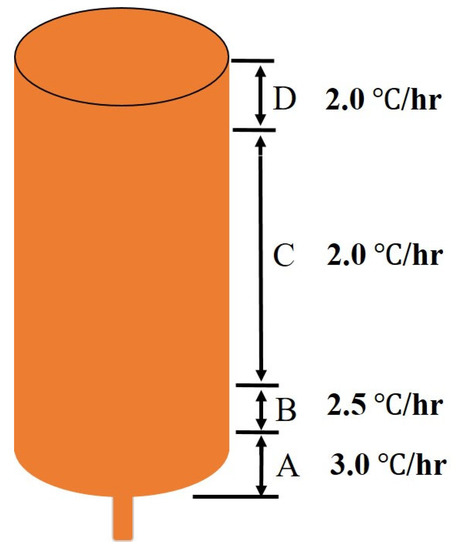
Figure 1.
Each compartment of GaAs ingot.
3. Design of Heater
In this study, the design of a heater for ingot growth was performed. Through internal temperature measurement, the temperature simulation model was developed, and the optimized heater was designed. It was planned for a device that could control the temperature to grow while maintaining an ideal interface along the interface on the solid–liquid boundary and not form the concave interface. If a concave interface occurred, twins and polycrystals were formed due to differences between the growth direction and the thermal expansion area, so a temperature gradient condition was derived that could minimize it. The concave occurs during the ingot growth process. This study simulated the 4-inch GaAs ingot growth process through the temperature simulation and examined the application condition of the heater to determine the optimal heater position.
It was constructed by a model for analyzing the VGF heater designed to predict heat transfer characteristics such as temperature distribution, thermal capacity, and insulation capability of VGF heaters, and the heat transfer analysis was carried out for them. The scope of heat transfer analysis for VGF heaters is from the heater winding, which is a heat source, to the heater’s inside space where heat is transferred, GaAs, the quartz case, which is the heat transfer path from the heat source to GaAs, pBN, the ceramic block for external insulation, cerakwool, and ambient air that is a heat sink.
The most important factor among the VGF heater’s heat transfer characteristics is the heat value of respective heaters that could form the temperature distribution desired for GaAs in the vertical direction. In addition, the adequacy of the heat transfer path and the insulation capability of the external case should be examined. If the insulation capability against the outside is insufficient, there is a problem where the heat value required for heaters is excessive. If the design of the heat transfer path is improper, the temperature distribution in the vertical direction of GaAs is not formed as required [7,8]. As in Figure 2, firstly, the heat generated from the heater winding is transferred by convection in the ambient air. In this way, heat transfer by convection occurs from the air with temperature rising to the surrounding wall surface. The heat transfer occurs by convection on the ceramic block, which is the external air direction, and the quartz wall surface, which is the GaAs direction, and they are solids, respectively, in which the heat is transferred by conduction. The heat transfer path from the heater winding, heat source, to the air, heat sink, in the horizontal direction is as in Figure 3. The heat resistance was defined using the following equation.
where is is total heat resistance. is the heat transfer coefficient of air in a heater. is the thermal conductivity of ceramic blocks. is ceramic block thickness. is the thermal conductivity of cerakwool. is cerakwool thickness. r is radius. A is area.
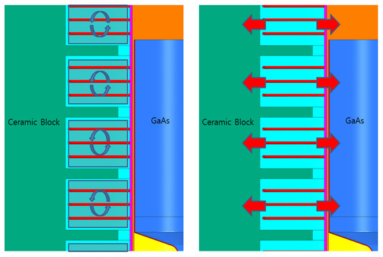
Figure 2.
Heat transfer of the air around the heater and heat transfer from the wall.
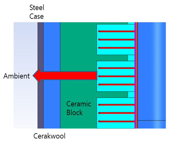
Figure 3.
Heat transfer from the heat source through the insulator to the heat sink.
The heat transfer coefficient between the air and the VGF heater wall surface, between the air inside the heater and the cerakwool is a function of the shape and temperature difference, and it is very difficult to control it in terms of the design. To increase the insulation effect against the outside, therefore, we need a design to apply materials with low thermal conductivity and increase the thickness. The heat transfer path from the heater for melting GaAs is as in Figure 4, and the heat transfer coefficient between the air and the quartz wall surface is difficult to control, like external insulation. Therefore, the thickness of quartz, vacuum, and pBN, which are solid thermal resistance, should be considered to perform the design. At this time, if the thickness of quartz and pBN, which are solid components, is greater, thermal resistance becomes larger in the horizontal direction. And the heat transfer between solids in a vertical direction increases, so it is difficult to control the temperature distribution in the vertical direction of GaAs. Therefore, it is best to minimize the thickness of solid components from a heat transfer performance perspective. Since the GaAs melted into the liquid phase should be solidified by crystallizing from the lower part, upward thermal resistance should be larger than downward thermal resistance. Therefore, the liquid-phased upper part of GaAs should be made up by vacuum to improve the insulation performance. Since it should be solidified from the lower part of GaAs, thermal resistance in the vertical downward direction should be relatively smaller than in other directions. Therefore, it is designed to conduct heat through alumina with high thermal conductivity. Heat is highly transferred by natural convection in the vertical direction by exposing this alumina to the outside atmospheric air. Figure 5 shows the heat transfer path in the upper and lower part. The final result was designed as a structure that arranges a total of eight heaters in the length direction. Figure 6 shows the design result of the heater for the GaAs ingot.
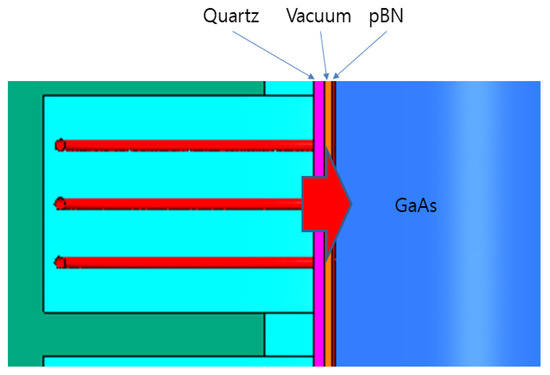
Figure 4.
Heat transfer path from heater winding to GaAs.
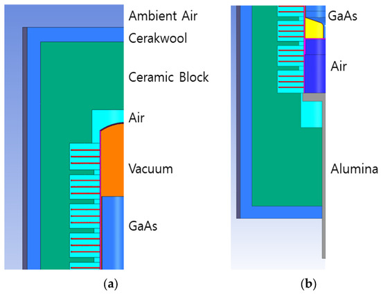
Figure 5.
Heat transfer path in the upper and lower part. (a) Upper part and (b) lower part.
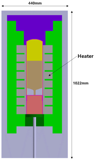
Figure 6.
Design result of heater for GaAs ingot.
4. Numerical Analysis and Manufacturing of Heater
Classical heat transfer analysis has limitations because the shape of the VGF heater designed is very complicated, so the numerical analysis method was used to carry out the heat transfer analysis. Since it is also needed to analyze the flux flow by natural convection, this analysis used ANSYS-CFX to perform the heat transfer analysis. For heat transfer analysis on VGF heaters, modeling for every component of the VGF heater was conducted, and elements with low importance were simplified. The grid generation of the models for each component of VGF heaters was carried out for finite element analysis. The solid components and the fluid components which could occur flux flow caused by natural convection were divided into models. For the fluid components, the boundary layer effect was considered to apply the structured grid to the interface part with the solid components. To save analysis time, the analysis model and grid generation were carried out for a quarter of the entire model. For the boundary condition for the heat source, heat flux was set on the surface area of the winding model so that the heat value of the heater winding should be within a maximum of 550 W. For the heat sink, an ambient condition of 20 °C, 1 atmosphere was applied to the upper part of the analysis target for the entire case model. Figure 7 shows modeling for numerical analysis. Figure 8 and Table 1 show boundary conditions. To apply heat transfer by natural convection, buoyancy was set, and gravitational acceleration was considered. The properties of the applied GaAs components and the air are shown in Table 2. In other words, Table 2 shows the properties of the fluid components. Properties of the applied GaAs solid form and other solid components are presented in Table 3. That is, Table 3 shows the properties of the solid components.
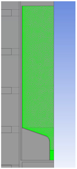
Figure 7.
The result of modeling for numerical analysis.
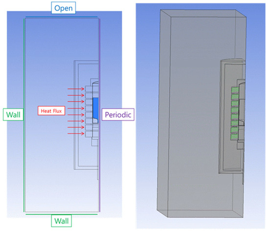
Figure 8.
Boundary conditions of modeling.

Table 1.
Each value of boundary conditions.
Table 2.
Properties of GaAs liquid and air.
Table 3.
Properties of solid materials.
The heat transfer analysis on the designed VGF heater was carried out for the two-step solidification process of GaAs. The analysis was performed to make the temperature of the GaAs interface between liquid and solid become melting and freezing temperature by controlling the heat flux on the winding surface of eight heaters arranged in a vertical direction. Since the heat transfer analysis was carried out with steady conditions, the radiant heat transfer was not considered. The result of the heat transfer analysis is shown in Figure 9, which shows the temperature contour of GaAs. For temperature simulation, the heat value of respective heaters and the adequacy of the heat transfer path were examined, which could form the desired temperature distribution of GaAs in a vertical direction that is the most important factor in the heat transfer characteristics, and it was considered the insulation capability of the outer case. As a result of the temperature simulation, it made area A have a temperature gradient of 3 °C/Cm and the corresponding growth rate was about 2.8 mm/hr, but as an experimental result, even if reducing it to half, the solid–liquid interface was kept flat, and the heat stress decreased, so it was examined to obtain a high-quality crystal in this compartment. In area B, the growth rate increased to 2 mm/hr. To prevent the solid–liquid interface shape from continuing to be convex, the temperature gradient was reduced to 2.5 °C/Cm for planarization. In area C, the growth rate was increased to 3 mm/hr, and the temperature gradient was reduced to 2 °C/Cm again. In area C, it was applied to minimize the heat stress occurrence on the rear of the ingot. The shape of the equipment with the ingot growth furnace heater designed and finally manufactured heater is presented in Figure 10.
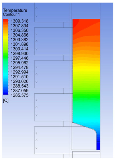
Figure 9.
Temperature contour of GaAs.
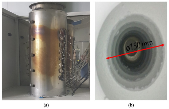
Figure 10.
The shape of the manufactured heater. (a) External shape and (b) internal shape.
The designed ingot growth furnace equipment was used to manufacture the final GaAs crystal through the GaAs ingot growth. This equipment was designed so that the heater’s inner diameter is 150 mm, internal temperature control is 1238 °C or more, the heater’s control positions eight zones, and its producing size could be implemented up to 4 inches. The GaAs ingot produced with this equipment was processed to complete the final substrate, which could be applied to micro LEDs. Figure 11 shows the GaAs ingot crystal produced through this study. Through this study, GaAs of 4 inches and 154 mm was manufactured. It developed products with high-quality characteristics below 750 EA/Cm2 EPD (etched pit density). The manufactured GaAs was polished and sliced to manufacture substrates. The GaAs ingot crystal was processed to manufacture the final wafer. Figure 12 shows the manufactured wafer. The roughness of the GaAs wafer was evaluated. The average value was investigated by evaluating the roughness of a total of five areas. The average value was found to be 0.057 nm. Thickness uniformity was analyzed through section thickness measurements. The thickness deviation is 1.11 μm. The carrier density was found to be 1.06 × 10¹⁸ CC/Cm3. The mobility value was investigated to be 4.06 × 10³ Cm2/Vs. The EPD was found to be 750 EA/Cm2. As a result of comparing the results of previous studies, carrier density, and mobility were improved. If more than 70% of heat energy is cooled to the lower part of the heat flow, a convex line is formed. In this study, temperature simulation was conducted to prevent the formation of concave lines. The measurement results were confirmed to be sufficiently valid. Table 4 shows the measurement results of GaAs ingot crystal.
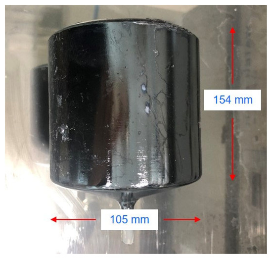
Figure 11.
The manufactured GaAs ingot crystal.
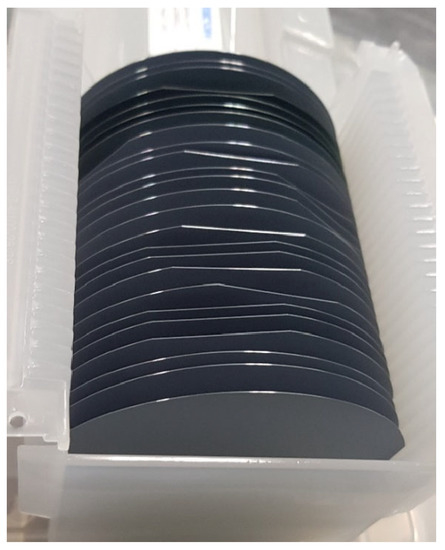
Figure 12.
The manufactured wafer.
Table 4.
The measurement result of roughness.
5. Conclusions
In this study, the GaAs ingot for micro LEDs was produced by applying the VGF method. The core of the production equipment is the heater applying heat. This study used the technology of controlling crystal growth temperature through temperature simulation to design the heater for producing 4-inch-large diameter GaAs. The technology that could sensitively cope with temperature change depending on the surrounding environmental change was developed based on temperature simulation technology. The result of numerical analysis on heat transfer was used to develop the VGF equipment embedded with a total of eight heaters. In addition, this study developed a technology that could minimize the rate of defects such as twin and poly and secure the optimum conditions on the solid–liquid interface during growth. The result of this study could be used to produce substrates that could be applied to optical devices and special purposes such as satellites and the military in the future.
Author Contributions
Y.P., conceptualization, software, validation, writing—original draft preparation; H.P., writing—review and editing and work guidance. All authors have read and agreed to the published version of the manuscript.
Funding
This research was supported by the Korea Institute for Advancement of Technology (KIAT) grant funded by the Korean Government (MOTIE) (P0012769, the Competency Development Program for Industry Specialist). Furthermore, this research was supported by the Korea Basic Science Institute (National Research Facilities and Equipment Center) grant funded by the Ministry of Education (Grant No. 2023R1A6C101B042).
Institutional Review Board Statement
Not applicable.
Informed Consent Statement
Not applicable.
Data Availability Statement
The data presented in this study are available upon reasonable request from the corresponding author.
Conflicts of Interest
The authors declare no conflict of interest.
Abbreviations
| latent heat of GaAs | |
| thermal conductivity of solid state | |
| thermal conductivity of fluid state | |
| total heat resistance | |
| heat transfer coefficient of air in heater | |
| thermal conductivity of ceramic block | |
| ceramic block thickness | |
| thermal conductivity of cerakwool | |
| cerakwool thickness | |
| r | radius |
| A | area |
References
- Hjort, K.; Soderkvist, J.; Schweitz, J.A. Gallium arsenide as a mechanical material. J. Micromech. Microeng. 1994, 4, 1. [Google Scholar] [CrossRef]
- Jantz, W.; Stibal, R.; Windscheif, J.; Wagner, J. Variation of material parameters along the growth direction of liquid encapsulated Czochralski grown GaAs ingots. Appl. Surf. Sci. 1991, 50, 480–484. [Google Scholar] [CrossRef]
- Greene, P. Growth of GaAs ingots with high free electron concentrations. J. Cryst. Growth 1980, 50, 612–618. [Google Scholar] [CrossRef]
- Metaferia, W.; Schulte, K.; Simon, J.; Johnston, S.; Ptak, A.J. Gallium arsenide solar cells grown at rates exceeding 300 µm h−1 by hydride vapor phase epitaxy. Nat. Commun. 2019, 10, 3361. [Google Scholar] [CrossRef] [PubMed]
- Dropka, N.; Böttcher, K.; Holena, M. Development and optimization of VGF-GaAs crystal growth process using data mining and machine learning techniques. Crystals 2021, 11, 1218. [Google Scholar] [CrossRef]
- Li, Z.; Kim, T.H.; Han, S.Y.; Yun, Y.J.; Jeong, S.; Jo, B.; Ok, S.A.; Yim, W.; Lee, S.H.; Kim, K.; et al. Wide-bandgap perovskite/gallium arsenide tandem solar cells. Adv. Energy Mater. 2019, 10, 1903085. [Google Scholar] [CrossRef]
- Weimann, H.; Amon, J.; Jung, T.; Müller, G. Numerical simulation of the growth of 2″ diameter GaAs crystals by the vertical gradient freeze technique. J. Cryst. Growth 1997, 180, 560–565. [Google Scholar] [CrossRef]
- Birkmann, B.; Rasp, M.; Stenzenberger, J.; Müller, G. Growth of 3″ and 4″ gallium arsenide crystals by the vertical gradient freeze (VGF) method. J. Cryst. Growth 2000, 211, 157–162. [Google Scholar] [CrossRef]
- Amon, J.; Berwian, P.; Müller, G. Computer-assisted growth of low-EPD GaAs with 3″ diameter by the vertical gradient-freeze technique. J. Cryst. Growth 1999, 198–199, 361–366. [Google Scholar] [CrossRef]
- Nikola, N.; Dallaev, R.; Talu, S.; Kastyl, J. Overview of the current ctate of gallium arsenide-based solar cells. Material 2021, 14, 3075. [Google Scholar] [CrossRef]
- Bakkar, A. Electrochemical synthesis of silicon and gallium arsenide photovoltaic thin films: A critical review and a novel approach. Mater. Sci. Forum 2020, 1008, 84–96. [Google Scholar] [CrossRef]
- Dropka, N.; Frank-Rotsch, C. Accelerated VGF-crystal growth of GaAs under traveling magnetic fields. J. Cryst. Growth 2013, 367, 1–7. [Google Scholar] [CrossRef]
- Marchenko, M.; Liu, W.; Badawi, M.; Yin, P. The influence of the scatter of heat flux at the m/c interface on the frequency of appearance of poly body and twin defects during 6″ semi-insulating GaAs crystal growth by the VGF method. J. Cryst. Growth 2008, 310, 2134–2140. [Google Scholar] [CrossRef]
- Kowalski, B.J.; Nietubyc, R.; Sadowski, J. Mn contribution to the valence band of Ga0.98Mn0.02Sb—A photoemission study. ACTA Phys. Pol. A 2022, 3, 175–179. [Google Scholar] [CrossRef]
- Börner, F.; Eichler, S.; Polity, A.; Krause-Rehberg, R.; Hammer, R.; Jurisch, M. Large-depth defect profiling in GaAs wafers after saw cutting. Sens. Appl. Surf. Sci. 1999, 149, 151–158. [Google Scholar] [CrossRef]
- Blevins, J.; Yang, G. On optical properties and scintillation performance of emerging Ga2O3: Crystal growth, emission mechanisms and doping strategies. Mater. Res. Bull. 2021, 144, 111494. [Google Scholar] [CrossRef]


Disclaimer/Publisher’s Note: The statements, opinions and data contained in all publications are solely those of the individual author(s) and contributor(s) and not of MDPI and/or the editor(s). MDPI and/or the editor(s) disclaim responsibility for any injury to people or property resulting from any ideas, methods, instructions or products referred to in the content. |
© 2023 by the authors. Licensee MDPI, Basel, Switzerland. This article is an open access article distributed under the terms and conditions of the Creative Commons Attribution (CC BY) license (https://creativecommons.org/licenses/by/4.0/).