Article

A Novel Secondary Side Series LCD Forward Converter with High Efficiency and Magnetic Reset

1
College of Electrical and Control Engineering, Xi’an University of Science and Technology, Xi’an 710054, China
2
College of Physics and Electrical Engineering, Weinan Normal University, Weinan 714000, China
*
Author to whom correspondence should be addressed.
Appl. Sci. 2023, 13(13), 7640; https://doi.org/10.3390/app13137640
Submission received: 23 April 2023 / Revised: 16 June 2023 / Accepted: 26 June 2023 / Published: 28 June 2023
(This article belongs to the Section Electrical, Electronics and Communications Engineering)

Abstract

:
A novel secondary side series LCD forward converter with a high efficiency and a magnetic reset is proposed in this paper. Compared with the traditional forward converter, the proposed converter can transfer excitation energy to the output terminal and achieve a reliable magnetic reset of the transformer with a better working efficiency. Moreover, the proposed converter realizes the low-voltage turn-on of the switch. The operating principle and energy transmission process of the proposed converter is explicitly analyzed. It was concluded that the optimal combined working mode was Lm-DCM, L1-CCM and L2-CCM. By analyzing the energy transmission mechanism of the proposed converter in the best working mode, the parameter design scheme of the proposed converter was obtained. Finally, a prototype was built. The simulation and experimental results are presented to verify the correctness of the theoretical analysis and the feasibility of the parameter design scheme of the proposed converter. At the same time, a comparison between the proposed converter and existing converters was conducted to demonstrate the best electrical performance of the proposed converter.

1. Introduction

Power converters are widely used in various instruments and electrical and electronic equipment. Currently, converters have a trend towards higher efficiency, higher power density, and higher reliability [1,2,3,4,5]. Depending on the circuit structure, the power converter can be divided into a non-isolation or an isolation structure. In common power supply systems, an isolation converter is usually selected. An important part of an isolated converter, the magnetic element can store energy and realize the input–output isolation, which is an essential factor affecting the electrical performance of the converter [6,7]. Common isolated converter topologies mainly include a forward converter and a flyback converter. However, the output power of the flyback converter is greatly limited and its efficiency is not high, so it is mostly used in low-power applications [8,9]. Compared to a flyback converter, the power of a forward converter is not limited by the energy storage capacity of the transformer. It exhibits a high working reliability and a relatively simple structure, and has been widely used in small and medium power fields.
Although forward converters have many advantages, there are still many problems that still need to be solved. The forward converter has no magnetic reset function, and hence, it is likely to cause magnetic core saturation and other problems [10]. Magnetic saturation causes the current flowing through the switch to increase sharply, which greatly limits the promotion of the forward converter. Therefore, it is necessary to consider adding specific magnetic reset circuits to avoid magnetic saturation. In order to further promote the application of the forward converter, it is necessary to solve the problem of magnetic reset and improve the energy utilization rate. Therefore, it is essential to study new magnetic reset methods.
To solve the problem of magnetic reset, an auxiliary winding reset mode was studied in [11], which returned energy to the input terminal. However, its additional auxiliary windings complicated the structure and design of the transformer and had a small duty cycle range. The switch was required to withstand higher voltages, making it difficult to achieve a large power output. In [12,13,14,15,16,17], a primary-side RCD magnetic reset mode was studied. The reset mode comprised a simple structure and the range of the duty ratio was greater than 0.5. However, the voltage stress of the switch was large and most of the energy was consumed on the clamping resistor, reducing the efficiency and increasing the difficulty of the heat dissipation design. In [18,19], an active clamp reset circuit was proposed. The advantage of this reset circuit was that it achieved the soft switching of the main and auxiliary switches, thus reducing circuit losses. However, its driving circuit was complex, and when the duty cycle was greater than 0.5, the voltage stress of the switch exceeded twice the input voltage. The reset circuits of the forward converter were located at the primary side of the transformer, and the excitation energy stored in the transformer during the conduction of the switch was either fed back to the input terminal or consumed. This part of the excitation energy was not fully utilized, which did not improve the efficiency of the converter. Based on the above mentioned research, it was necessary to continuously improve the reset mode. The new reset method considers placing the reset circuit on the secondary side of the transformer to improve the energy utilization rate and achieve the goal of continuously optimizing the performance of the forward converter. In [20,21], a four-diode forward-flyback converter was proposed, which realized the transfer of the excitation energy to the load and improved the conversion efficiency of the transformer. However, four diodes were used in the circuit, which increased the cost and circuit loss of the converter. Within the entire dynamic range, the forward inductor only operated in a DCM, which was not suitable for a high power output. In [22], a full-bridge rectifier forward converter with a capacitor on the secondary side was proposed, which solved the issue where the inductor in a four-diode structure was unable to work in a continuous conduction mode. However, compared to the traditional forward converter, this topology increased the circuit loss and the voltage stress of the switch was significant, which was not conducive to the selection of the switch. In [23], a resonant forward reset topology with an auxiliary switch on the secondary side was developed, which reduced the losses of the switches and diodes. However, this topology used two switches, increasing the complexity of the control drive circuit. The secondary reset mode transmitted the excitation energy to the load, but there were still some problems, such as complicated circuit structure, the low output power of the converter, and the high voltage stress of the switch. Therefore, it is of great guiding significance to the propose a forward converter that can not only ensure the reliable reset of the magnetic core but also improve the electrical performance.
Based on forward converters that are unable to be magnetically reset, this paper proposes a new type of secondary side series LCD forward converter by studying the magnetic reset technology of secondary winding. The operation mode of the proposed novel forward converter was deeply studied, the optimal operating mode of the proposed converter was obtained, and the energy transmission mechanism under the optimal working mode was analyzed. It was concluded that the proposed converter can not only transfer the excitation energy to the output terminal, achieve a reliable magnetic reset of the transformer, and improve the work efficiency, but also achieve a low-voltage conduction of the switch and reduce the switching loss. According to the influence of the component parameters on the electrical performance of the converter in the best working mode, the corresponding parameter design method was established. Finally, according to the proposed parameter design method, an experimental prototype of the proposed converter was developed, and its working characteristics, output ripple, and efficiency were tested. The experimental results verified the correctness and feasibility of the proposed secondary side reset method.

2. Circuit Composition and Energy Transmission Process of a Novel of Secondary Side Series LCD Forward Converter

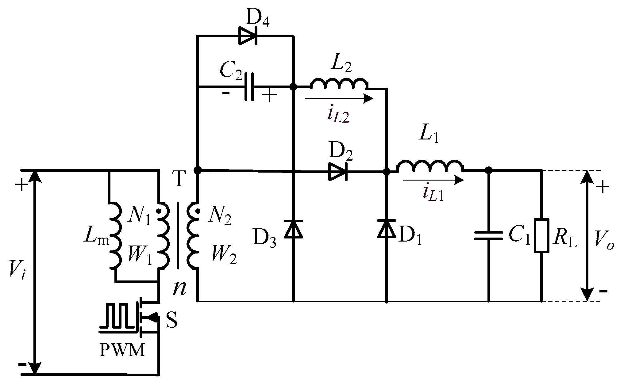
2.1. Composition and Principle of a Circuit

The schematic diagram of a novel secondary side series LCD forward converter is shown in Figure 1. Its circuit structure adds an LCD excitation energy transfer path (composed of D3, D4, C2, and L2) to the secondary side of the traditional forward converter. The proposed converter consists of a power switch S, two inductors (forward inductor L1 and auxiliary inductor L2), two capacitors (an output filter capacitor C1 and an additional capacitor C2), four diodes (D1–D4), a transformer T (consists of magnetizing inductor Lm and primary and secondary windings W1 and W2), and one resistive load RL. The magnetizing current coupled to W2 charges C2 through D3. Then, the capacitor C2 exchanges energy with the inductor L2 and the excitation energy is stored in the inductor L2. Finally, the inductor L2 transfers energy to the load through D3, thus realizing the reliable magnetic reset of the transformer.
To simplify the analysis of the operating principle of the novel secondary side series LCD forward converter, the following assumptions were made.
(1) The switch, diodes, inductors, and capacitors were considered to be ideal.
(2) The transformer leakage inductance was minimal, and the energy loss caused by the leakage inductance was not considered.
(3) The output voltage was assumed to be constant.
The magnetic reset circuit of the proposed converter can effectively transfer excitation energy to the load, improving the conversion efficiency of the converter. The working process was as follows.
During the switch-on period, the input voltage Vi was applied across the primary winding of the transformer. The energy was transferred to the load through the secondary winding of the transformer and iL1 increased linearly. At the same time, due to the conduction of D2, the capacitor C2 exchanged energy with the inductor L2. When the voltage across C2 dropped to zero and the switch S was still on, diode D4 was naturally turned on. Since diode D2 remained on, C2 and L2 were short-circuited, and the current flow through L2 remained unchanged. The forward energy continued to be supplied to the load through D2 and L1, and iL1 continued to increase until S was turned off and the stage ended. At this stage, the zero-voltage natural conduction of diode D4 was realized.
During the switch-off period, D3 was forward biased and D4 was reverse biased. The excitation energy was released to the capacitor C2 via D3, the voltage across C2 gradually increased from the minimum value, and the excitation energy was delivered to the capacitor C2, thus ensuring the reliable magnetic reset of the transformer core. Meanwhile, the inductor L1 transferred energy to the load through D1, and iL1 gradually decreased. Since diodes D1 and D3 were in on state, iL2 remained unchanged until iL1 decreased to be equal to iL2 and diode D1 was naturally turned off, thus realizing the zero-current turn-off of D1. After that, if D3 still remained conductive, iL1 and iL2 continued to flow through D3 until the switch was turned on, iL1 and iL2 decreased to the minimum value, the voltage across C2 reached its maximum value, and the excitation current decreased to the minimum value. If the excitation current decreased to zero before the switch was turned on, all the excitation energy of the transformer was released to C2, and the voltage across C2 increased to the positive the maximum value. Subsequently, the energy stored in the capacitor C2 was delivered to L2 and W2 through diode D1, and the currents flowing through inductor L2 increased. At the same time, the inductor L1 continued to supply energy to the load via D1 until iL2 increased to be equal to iL1 and the diode D1 was turned off. Then, C2, W2, L1, and L2 supplied energy to the load together. When the voltage across C2 decreased to lower than Vo, the excitation inductor generated a voltage with the same polarity as the primary side and the proposed converter achieved a low-voltage turn-on of the switch.

2.2. Analysis of the Working Mode and Energy Transfer Process of the Converter

Depending on whether the excitation current decreases to zero during the switch-off period, the excitation inductance can be divided into a continuous conduction mode (CCM) and a discontinuous conduction mode (DCM). At the same time, according to the working principle of the converter, when iL2 and iL1 are equal, they will jointly supply energy to the load. Therefore, through the analysis of the working principle of the converter, the inductors L1 and L2 can only work in CCM or DCM at the same time. To realize a high power transmission, improve the energy transmission efficiency, and reduce the switching loss, it is necessary to choose the best working mode of the converter.
When Lm works in the CCM, the secondary winding transfers energy to the capacitor C2 through D3 during the switch-off period, and the voltage across C2 reaches the maximum value when the switch is turned on. Therefore, the voltage stress of the switch in this mode is much higher than the input voltage. When Lm operates in the DCM, the secondary winding W2 delivers energy to the capacitor C2 via diode D3 until the excitation current decreases to zero. The voltage across the capacitor C2 reaches the maximum value. After that, the capacitor C2 transfers energy to the load through L1, L2, and W2 until the voltage across C2 decreases lower than the output voltage. At this time, the voltage at both ends of the secondary winding W2 is changed to a positive direction voltage. Therefore, at the moment when the switch is turned on, the drain source of the switch is lower than the input voltage Vi, and the proposed converter can achieve a low-voltage turn-on of the switch. Therefore, in order to reduce the switching loss, Lm was selected to work in the DCM. At the same time, in order to achieve a large energy transmission with the proposed converter, it was necessary to ensure that one of the inductors, L2 or L1, operates in the CCM. Since L1 and L2 can only work in the CCM or DCM simultaneously, L1 and L2 were selected to work in the CCM. Therefore, it was concluded that the optimal working mode of the proposed converter was Lm-DCM, L1-CCM, and L2-CCM.
The waveform of the proposed converter operating in the optimal operating mode is shown in Figure 2. As shown in Figure 2, the working process of the converter can be divided into six stages in one cycle. The energy transmission characteristics of each stage were specifically analyzed as follows.
Phase I [t0~t1]: At t0, the switch S was turned on, and the positive voltage across the secondary side, coupled from Vi through the transformer, was Vi/n. At this time, D2 was forward biased, while D1, D3, and D4 were reverse biased. L1 was magnetized from the voltage of the secondary winding W2 of the transformer and iL1 increased linearly from the minimum value with a slope of (Vi/nVo)/L1. Due to the conduction of D2, C2 and L2 resonated through D2, and the capacitor C2 transferred energy to the inductor L2 until the voltage across C2 decreased to zero.
Phase II [t1~t2]: At t2, after the voltage across C2 decreased to zero, diode D4 was naturally turned on as diode D2 continued to be turned on and iL2 remained unchanged. At the same time, the forward energy continued to be provided to the load and the inductor L1 through D2, and iL1 continued to rise linearly. This mode was completed at t2 when iL1 reached the maximum value.
Phase III [t2~t3]: At t2, S was turned off, D3 was forward biased, and D4 was reverse biased. The secondary winding W2 delivered the excitation energy to the capacitor C2 and the voltage across C2 increased from zero. D1 conducted a freewheeling loop for L1 and its current iL1 decreased linearly from the maximum value. L2 was short-circuited due to the conduction of D1 and D3, and iL2 continued to remain unchanged until iL1 decreased to be equal to iL2. This mode ended at t3 when iLm reached zero and the transformer core was reset.
Phase IV [t3~t4]: This mode began when the voltage across C2 reached the maximum value, the energy stored in the capacitor C2 was released to W2 via D3, and the current iL1 continued to decrease linearly until iL1 decreased to be equal to iL2. Hence, D1 was turned off at the end of this mode.
Phase V [t4~t5]: At t4, L1 and L2 were connected in a continuous series to supply energy to the load through D3, and iL1 and iL2 decreased linearly. At the end of this mode, the currents flowing through inductors L1 and L2 were equal to the current flowing through C2.
Phase VI [t5~t6]: At t5, D3 was turned off, the energy stored in capacitor C2 was released to L1, L2, and W2, and iL1 and iL2 gradually increased. During this mode, if the voltage across C2 equaled the output voltage Vo and the voltage polarity across the secondary side was changed to the positive direction, C2, L1, L2, and W2 delivered energy to the load simultaneously. At the end of this interval, the voltage stress on the power switch was lower than the input voltage Vi; that is, the switch achieved a low-voltage turn-on.

3. Selection and Analysis of the Additional Capacitance Parameters When the Excitation Inductor Works in the DCM

During the switch-off period, the magnetizing current coupled to the secondary winding charged C2 through D3, and the voltage across C2 increased from zero. Its equivalent circuit is shown in Figure 3.
According to Figure 3, we can obtain the following equation.
u C 2 ( t ) u W 2 ( t ) = 0
The currents flowing through the capacitor C2 and the secondary excitation winding W2 can we written as the following.
i C 2 = i W 2 = C 2 d u C 2 ( t ) d t
The voltage across the secondary side can be obtained from Equation (2).
u W 2 ( t ) = L W 2 C 2 d 2 u C 2 ( t ) d t 2
Substituting Equation (3) into Equation (1), we can derive the following equation.
u C 2 ( t ) + L W 2 C 2 d 2 u C 2 ( t ) d t 2 = 0
At the moment when the switch is turned off, the current flowing through the secondary winding W2 is nILm,max′ and the voltage across C2 is equal to zero. Therefore, the initial conditions of u C 2 ( 0 ) = 0 and u C 2 ( 0 ) = n I L m , max / C 2  can be obtained. According to these initial conditions, we can obtain the following by solving Equation (4).
u C 2 ( t ) = n I L m , max L W 2 C 2 sin t L W 2 C 2
where n = N1:N2 represents the turn ratio of the transformer.
By solving Equation (5), the current flowing through C2 can be obtained as follows.
i C 2 ( t ) = n I L m , max cos t L W 2 C 2
From Equation (6), the time for the excitation current to decreased from the maximum value to zero can be obtained as follows.
t L m = π L W 2 C 2 2
When Lm works in the DCM, the magnetizing inductor current increases linearly from zero to the maximum value during the conduction of the switch. We can obtain the expressions for ILm,max′ using the following equation.
I L m , max = V i L m D T
Here, D represents the duty cycle.
Substituting Equations (7) and (8) into Equation (5), the maximum voltage across C2 can be calculated using the following equation.
V C 2 , max = V i D T L m C 2
where LW2 = Lm/n2 is the secondary side inductance.
According to Equation (9), the maximum voltage stress of the switch can be obtained using the following.
V ds DCM = V i + n V C 2 , fmax = V i + n V i D T L m C 2
To ensure that the excitation energy is completely transferred to the capacitor C2 during the switch-off period, the time for the excitation current to decrease to zero should be less than the switch-off time (1 − D)T. Therefore, we can obtain the value using the following equation.
t L m ( 1 D ) T
By substituting Equation (7) into Equation (11), the value range of the capacitor C2 can be calculated using the following equation.
C 2 4 n 2 ( 1 D ) 2 π 2 f 2 L m

4. Analysis of the Voltage Characteristics of the Switch and the Selection of the Forward Inductance Parameter

4.1. Analysis of the Turn-Off Characteristics of the Switch

During the switch-on period, D2 was in on state, the inductor L2 and the capacitor C2 resonated in series, and the equivalent circuit is shown in Figure 4.
According to Figure 4, we can obtain the following equation.
u C 2 ( t ) + L 2 C 2 d 2 u C 2 ( t ) d t 2 = 0
When the switch is turned on, the current through C2 increases from IL1,t0 and the voltage across C2 decreases from VC2,t0. Therefore, the initial conditions u C 2 ( 0 ) = V C 2 , t 0 and u C 2 ( 0 ) = I L 1 , t 0 C 2 can be obtained. According to these initial conditions, we can obtain the following by solving Equation (13).
u C 2 ( t ) = V C 2 , t 0 cos t L 2 C 2 I L 1 , t 0 L 2 C 2 sin t L 2 C 2
Since IL1,t0 is approximately zero at the moment when the switch is turned on, by solving Equation (14), the time for the voltage across C2 drop to zero can be obtained using the following equation.
t m = π L 2 C 2 2
To ensure that the switch is turned off at a lower voltage, the voltage across C2 should be reduced to zero before the switch is turned off. Therefore, tm should be less than the switch-on time dT, which can be obtained using the following equation.
π L 2 C 2 2 d T
According to Equation (16), L2 should satisfy the following.
L 2 4 D 2 π 2 f 2 C 2

4.2. Analysis of the Switching Characteristics of the Switch

According to Equation (14), the current flow through the inductor L2 can be derived using the following.
i L 2 ( t ) = C 2 d ( u C 2 ( t ) ) d t = I L 1 , t 0 cos t L 2 C 2 + V C 2 , t 0 L 2 C 2 sin t L 2 C 2
The inductor current of IL2,t1 at the switch-off time can be obtained using the following.
I L 2 , t 1 = I L 1 , t 0 cos t m L 2 C 2 + V C 2 , t 0 L 2 C 2 sin t m L 2 C 2
During the switch-on period, iL1 increases linearly from IL1,t0, and reaches the maximum value at the switch-off time. The maximum current of inductor L1 can be obtained using the following.
I L 1 , max = I L 1 , t 0 + V i n V o n L 1 D T
Due to the simultaneous conduction of diodes D1 and D3, the series branches of the inductor L2 and diode D4 are short-circuited, so iL2 remains unchanged during this process until iL1 decreases to be equal to iL2 and this process ends. In this process, the inductor L1 supplies energy to the load through D1, iL1 decreases linearly, and the expression of iL1 is shown in Equation (21).
i L 1 ( t ) = I L 1 , max V o L 1 t
According to Equations (20) and (21), when iL1 decreases to be equal to iL2, the required time t1 can be obtained using the following equation.
t 1 = n L 1 ( I L 1 , t 0 I L 2 , t 1 ) + ( V i n V o ) D T n V o
When iL1 drops to be equal to iL2, D1 is naturally turned off. After that, L1 and L2 deliver energy to the load through diode D3. The equivalent circuit is shown in Figure 5.
As shown in Figure 5, iL1 and iL2 decrease linearly from IL2,t1 until the charging voltage across C2 increases to the maximum value, iL1 and iL2 decrease to the minimum value, and this process ends. We can obtain the expression for iL1 and iL2 using the following equation.
i L 1 - 2 ( t ) = I L 2 , t 1 V o L 1 + L 2 t
According to Equations (7) and (22), the time t2 for L1 and L2 to jointly transfer energy to the load can be calculated using the following equation.
t 2 = t L m t 1 = π L W 2 C 2 2 n L 1 ( I L 1 , t 0 I L 2 , t 1 ) + ( V i n V o ) D T n V o
By substituting Equation (24) into Equation (23), the minimum value of iL1 can be obtained using the following.
I L 1 , min = I L 2 , t 1 V o L 1 + L 2 π L W 2 C 2 2 n L 1 ( I L 1 , t 0 I L 2 2 ) + ( V i n V o ) D T n V o
When the voltage across C2 reaches the maximum value, the energy stored in the capacitor C2 is released to inductors L1, L2, and W2, and its equivalent circuit is shown in Figure 6.
According to Figure 6, we can obtain the following equation.
u C 2 ( t ) + u L 2 ( t ) + u L 1 ( t ) + u W 2 ( t ) + V o = 0
The voltage across L1, L2, and W2 can be derived as follows.
u L 2 = L 2 C 2 d 2 u C 2 ( t ) d t 2 u L 1 = L 1 C 2 d 2 u C 2 ( t ) d t 2 u W 2 = L W 2 C 2 d 2 u C 2 ( t ) d t 2
By substituting Equation (27) into Equation (26), we can obtain the following.
u C 2 ( t ) ( L L 2 + L L 1 + L W 2 ) C 2 d 2 u C 2 ( t ) d t 2 + V o = 0
According to the initial conditions u C 2 ( 0 ) = V C 2 , max , u C 2 ( 0 ) = I L 1 , min C 2 , by solving Equation (28), the voltage expression of C2 can be obtained using the following.
u C 2 ( t ) = I L 1 , min L 2 + L 1 + L W 2 C 2 sin t L 2 + L 1 + L W 2 C 2 + V C 2 , max V o cos t L 2 + L 1 + L W 2 C 2 + V o
From Equation (7), the time t3 for the capacitor C2 the deliver energy to L1, L2, and W2 during the switch-off period can be calculated using the following equation.
t 3 = ( 1 D ) T t m = ( 1 D ) T π L W 2 C 2 2
By substituting Equations (9) and (30) into Equation (29), the voltage across the capacitor C2 at the switch-on time can be obtained using the following.
V C 2 2 = I L 1 , min sin λ L 1 + L 2 + L W 2 ) C 2 + V i d T 2 L m C 2 V o cos λ L 1 + L 2 + L W 2 ) C 2 + V o
where λ = ( 1 d ) T π L W 2 C 2 2 .
According to Figure 6, the voltage across the secondary winding W2 can be calculated using the following equation.
V W 2 = V C 2 2 V o L W 2 L 2 + L 1 + L W 2
When the switch is turned on, the voltage across the primary side is nVW2, coupled from VW2 through the transformer, which is opposite to the polarity of the input voltage. Therefore, the voltage stress of the switch S can be obtained using Equations (31) and (32).
V ds = V i n V W 2 = V i + I L 1 , min L m 1 2 C 2 ( n 2 L 1 + n 2 L 2 + L m ) sin ( n λ n 2 L 1 + n 2 L 2 + L m ) C 2 n V i d T n 2 L 1 + n 2 L 2 + L m L m C 2 n V o L m n 2 L 1 + n 2 L 2 + L m cos n λ n 2 L 1 + n 2 L 2 + L m ) C 2
From the above analysis, we can see that the proposed converter can achieve a low-voltage turn-on of the switch, and the additional LCD can transmit both the excitation energy and the forward energy.

4.3. Parameter Design of the Forward Inductor L1

According to Figure 1, the current across the inductor L1 in one cycle is equal to the output average current, which can be drawn as the following.
I L 1 = I 0
The ripple of the inductor current iL1 can be given as the following.
Δ i L 1 = V i n V o n L 1 d T
According to Equations (34) and (35), the maximum current and minimum current of the inductor L1 can be obtained using the following.
I L 1 , max = I 0 + 1 2 Δ i L 1 = I 0 + D ( V i n V o ) 2 n L 1 f I L 1 , m in = I 0 1 2 Δ i L 1 = I 0 D ( V i n V o ) 2 n L 1 f
To operate the proposed converter in the best working mode, the minimum current of the inductor L1 should be less than the peak current of the inductor L2. From Equations (18) and (36), L1 should satisfy the following.
L 1 V i n V o 2 n ( V o R V i D T L m ( L 2 + L W 2 ) ) D T

5. Simulation and Experimental Analysis

5.1. Simulation Analysis

To verify the theoretical analysis, a PSIM simulation was built. The simulation results of the proposed converter were obtained from PSIM to verify the theoretical analysis preliminarily, and the index requirements of the experimental prototype are shown in Table 1.
According to the index requirements of the experimental prototype, assuming that the maximum duty cycle of the converter was 0.45, the number of turns of the primary winding turns was N1 = 30, the number of turns of the secondary winding was N2 = 13, and the excitation inductor Lm = 3.5 mH when the minimum DC input voltage was 198 V. According to Equation (12), we obtained 0 < C2 < 25 nF.
Considering the impact of the actual capacitance and the PCB parasitic capacitance, the capacitor C2 was taken as 10 nF in this experiment. According to Equation (17), we obtained 0 < L2 < 162.5 µH. Considering its volume and winding loss, L2 = 45µH was selected in this experiment. Under the condition that the inductor L2 was already present, the inductor L1 was taken as 50 µH, according to Equation (37).
Figure 7 shows the key waveforms of the proposed converter with the output currents of 2 A, 5 A, and 10 A, respectively. As shown in Figure 7a, the inductor current waveforms iL1 and iL2 affirmed that the inductor L1 and L2 operated in the CCM. The voltage waveform Vds affirmed that the voltage across the capacitor C2 increased first and then decreased during the switch-on period, indicating that Lm operated in the DCM. Using the voltage waveform of Vds, we concluded that the proposed converter achieved a low-voltage turn-on of the switch. Similarly, as shown in Figure 7b,c, it can be concluded that the inductor L1 and L2 also worked in the CCM, and the voltage stress waveform of Vds also increased first and then decreased during the switch-on period. Therefore, the excitation inductor Lm worked in the DCM, which was in good agreement with the theoretical results.

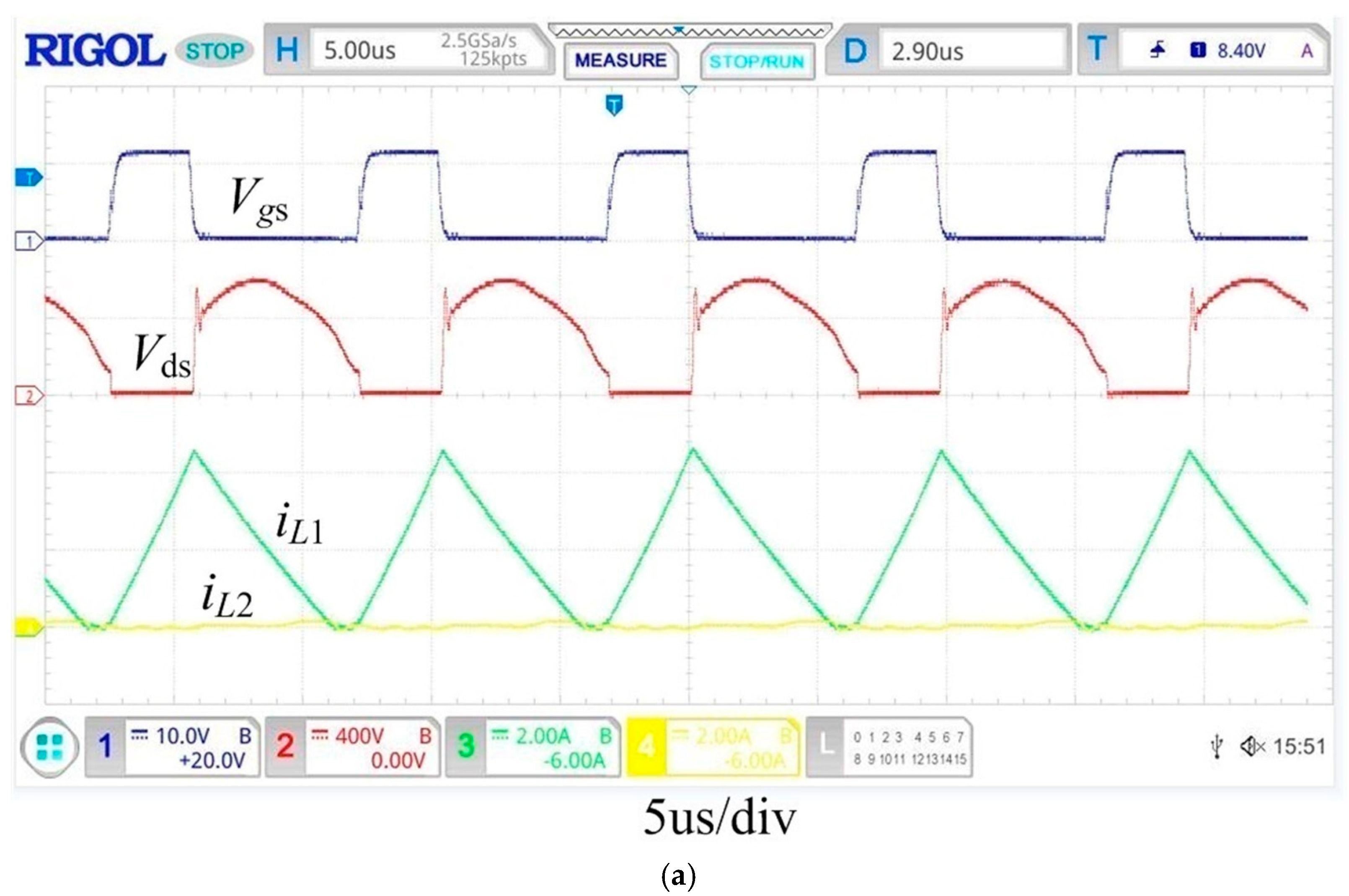
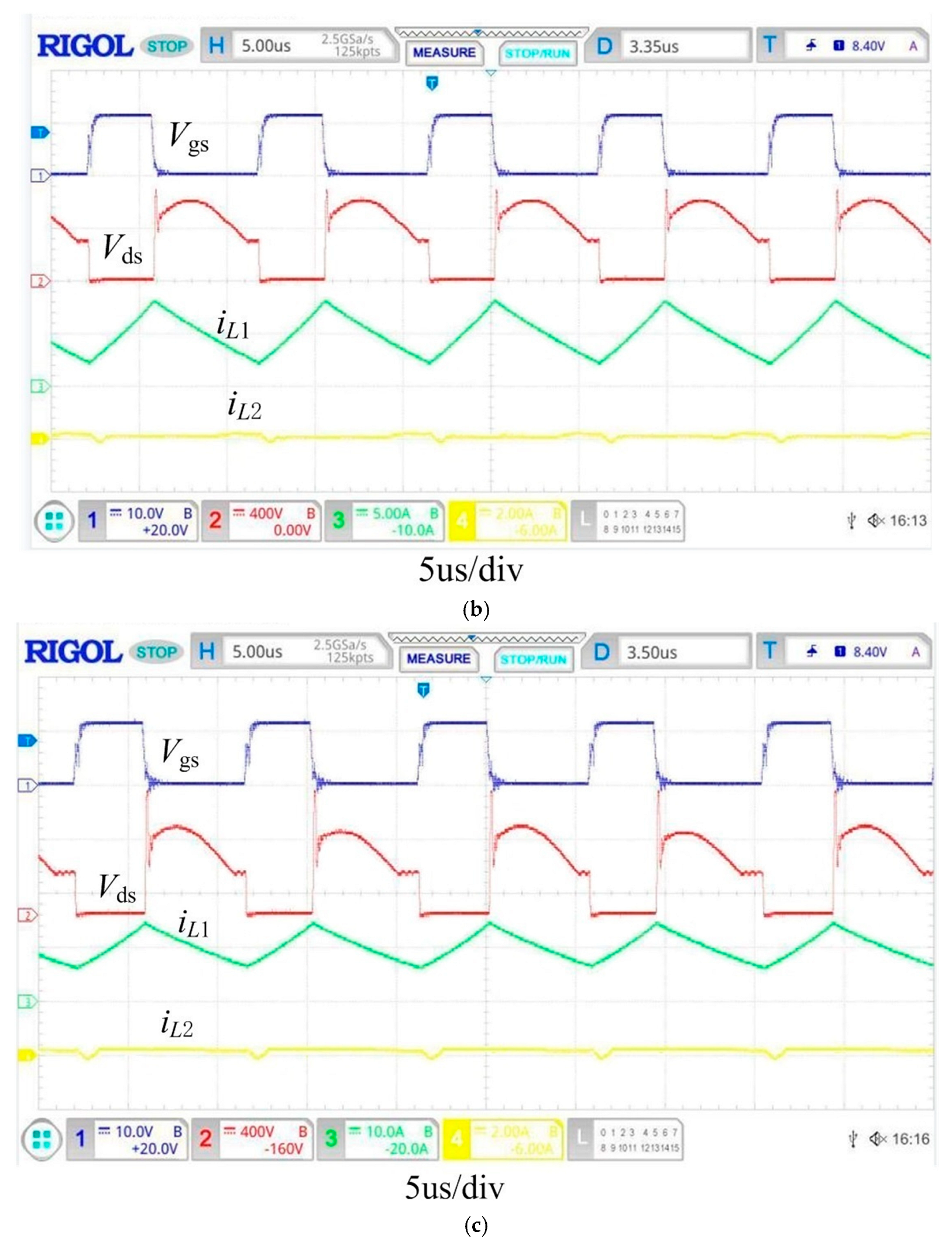
5.2. Experimental Analysis

In order to verify the performances and simulations further, we considered the following factors, such as the circuit power, efficiency, and output voltage ripple. The experimental prototype was developed, as shown in Figure 8. The key parameters were same as the simulated parameters. According to the working principle of the proposed converter and the existing equipment and safety practices in the laboratory, the selected parameters of the model are given in Table 2.
In order to verify the correctness of the optimal operating mode of the converter and its parameter design method, when the input voltage was DC300V, the waveforms of Vgs, Vds, iL1, and iL2 with output currents of 2 A, 5 A, and 10 A, respectively, were tested using the experimental prototype, as shown in Figure 9.
As shown in Figure 9, the voltage waveform of Vds first increased in a curve and then decreased in a curve during the switch-off period, indicating that Lm operated in the DCM. However, the inductor currents iL1 and iL2 were greater than zero throughout the entire switching period, indicating that the inductors L1 and L2 both operated in the CCM, which proves that the proposed converter operated in the optimal operating mode. At the same time, it can be seen in Figure 9 that when the output current of the converter was significant, the voltage stress on the power switch was equal to the input voltage at the switch-on moment. When the output current of the converter was minimal, the voltage stress of the switch was obviously lower than the input voltage at the switch-on moment. The above analysis shows that the proposed converter achieved a low-voltage turn-on of the switch. Therefore, the correctness of the above mentioned optimal working mode and its parameter design method was verified. Meanwhile, by comparing the experimental waveform with the simulated waveform, it can be seen that they were generally consistent.
According to the performance index requirements of the prototype, under an input voltage of 220 VAC, the output voltage was tested using different load conditions. Table 3 shows the experimental results of the proposed converter.
Table 3 presents the maximum variation when the output voltage was 0.23 V. Therefore, the load adjustment rate of the experimental prototype was obtained as the following.
U = Δ V o V o = 48.14 - 47.91 48 = 0.47 %
From Equation (38), it can be seen that the load adjustment rate of the developed experimental prototype met the design requirements.
The output ripple was an important technical index of the converter. According to the design index of the prototype, the output ripple voltage should be less than 1%Vo; that is, the output ripple voltage should be less than 480 mV. The waveform of the output ripple voltage was tested using full load conditions, as shown in Figure 9.
As shown in Figure 10, the peak-to-peak output voltage ripple of the proposed converter was 200 mV, which was less than 1%Vo. Therefore, the prototype designed in this paper met the index requirements of the converter.
To verify the working efficiency of the proposed converter, the efficiency of the experimental prototype was tested using changing output current conditions, and the measured efficiency is plotted in Figure 11.
Figure 11 shows that the proposed converter had a higher efficiency than the other converters under the medium and high power conditions, and the highest experimental efficiency reached was 93.5%, which met the index requirements of the converter. The energy of the converter was effectively utilized.
The comparison between the proposed converter and the other existing converters is presented in Table 4. The efficiency of the proposed converter was obviously higher than the efficiency of the other types, such as the converters proposed in [17,21]. The proposed converter utilized a lower number and the same number of components, respectively. In comparison with the converter proposed in [17,18], the number of active switches was fewer, which denoted that the complexity of the control circuit and the number of gate drivers was reduced due to the lower number of power switches. In comparison with the converter in [21], the voltage stress of the power switch of the proposed converter was adjustable with the change of the additional capacitor C2. In comparison with the converter in [17,18], the proposed converter transmitted excitation energy and forward energy to the load end, which improved the conversion efficiency of the transformer. In summary, the proposed converter exhibited the best electrical performance.

6. Conclusions

This paper proposed a new secondary side series LCD forward converter. The principal operation and energy transmission process of the proposed converter were presented, and it was concluded that the optimal operating mode of the proposed converter was Lm-DCM, L1-CCM, and L2-CCM. The value range of the capacitor C2 in the best working mode of the converter was analyzed, combining the analysis of the turn-on and turn-off characteristics of the switch, and the parameter design scheme of the converter was obtained. Finally, the proposed converter was implemented and tested in the best working mode and its performance was verified through the experimental results. The experimental results showed that its maximum efficiency was 93.5%, the output ripple voltage was less than 1% Vo, and the voltage adjustment rate was 0.47%. It was proved that the proposed converter possessed the merits of transferring excitation energy to the output terminal, the reliable magnetic reset of the transformer and an improvement in the working efficiency, and the realization of the low-voltage turn-on of the switch. This converter can be a good complement for the existing forward converters and an appropriate candidate for industrial applications.

Author Contributions

Conceptualization, G.Z. and S.L.; methodology, S.L.; software, G.Z.; validation, G.Z. and S.L.; writing—original draft preparation, G.Z.; writing—review and editing, G.Z. and S.L.; supervision, S.L.; project administration, S.L. All authors have read and agreed to the published version of the manuscript.

Funding

This work was supported by the National Natural Science Foundation of China [Grant Number 51777167], the Ministry of Education’s Industry School Cooperation Collaborative Education Project [Grant Number 220506298205949], the Weinan Research Project [Grant Number 2020ZDYF-JCYJ-24], and the Weinan High Quality Development Project [Grant Number WXQY002-009].

Institutional Review Board Statement

Not applicable.

Informed Consent Statement

Informed consent was obtained from all subjects involved in the study.

Data Availability Statement

The data used to support the findings of the study are available from the corresponding author upon request.

Acknowledgments

We gratefully acknowledge the work of the members of our laboratory at Xi’an University.

Conflicts of Interest

The authors declare no conflict of interest.

References

  1. Pol, P.V.; Patil, S.L. A High Efficiency Modified Forward Converter for Solar Photovoltaic Applications. Electr. Power Compon. Syst. 2023, 51, 525–537. [Google Scholar] [CrossRef]
  2. Kim, C.E.; Baek, J.; Lee, J.B. Improved Three Switch-Active Clamp Forward Converter With Low Switching and Conduction Losses. IEEE Trans. Power Electron. 2019, 34, 5209–5216. [Google Scholar] [CrossRef]
  3. Abareshi, M.; Hamzeh, M.; Farhangi, S.; Alavi, S.M. Robust control of a forward-converter active battery cell balancing. IET Power Electron. 2023, 16, 1271–1280. [Google Scholar] [CrossRef]
  4. Ghorbanian, M.; Maghsoudi, M.; Esteki, M.; Farzanehfard, H. Forward converter using a resonant auxiliary circuit to provide soft-switching and reset the magnetic core. IET Power Electron. 2022, 15, 1713–1724. [Google Scholar] [CrossRef]
  5. Phillips, A.; Cook, T.; West, B.; Grainger, B.M. Gallium Nitride Efficacy for High-Reliability Forward Convertersin Spacecraft. IEEE J. Emerg. Sel. Top. Power Electron. 2022, 10, 5357–5370. [Google Scholar] [CrossRef]
  6. Zhang, Z.G.; Liao, M.Y.; Jiang, D.R.; Yang, X.B.; Li, S. High step-up isolated forward-flyback DC/DC converter based onresonance with pulse frequency modulation. J. Power Electron. 2021, 21, 483–493. [Google Scholar] [CrossRef]
  7. Li, H.Z.; Liu, X.Y.; Li, H.F.; Lan, T.W. Analysis and Design Criteria of Integrated Magnetics in Forward Converter. Proc. CSEE 2019, 39, 3667–3675. [Google Scholar]
  8. Gao, S.S.; Song, H.K.; Wang, Y.; Xu, R.; Xu, D.G. A Secondary-Resonance MHz Active-Clamp Flyback Converter with Partial Power Processing. IEEE Trans. Ind. Appl. 2022, 58, 7988–7997. [Google Scholar] [CrossRef]
  9. Ghazali, M.; Adib, E.; Ting, C.Y. Efficient Soft Switching Single-Stage PFC for Low-Power Applications. IEEE J. Emerg. Sel. Top. Power Electron. 2023, 11, 818–825. [Google Scholar] [CrossRef]
  10. Li, H.Z.; Fan, L.L. Dual-tube Forward Converter with Electromagnetic Integration of Various Magnetic Materials. J. Electr. Eng. 2022, 17, 148–155. [Google Scholar]
  11. Chen, D.L.; Fan, Y.P.; Yan, Y.G. Research on Magnetic Reset Technique of Forward Converters. Power Electron. 1998, 1, 36–41. [Google Scholar]
  12. Wu, H.F.; Xing, Y. Families of Forward Converters Suitable for Wide Input Voltage Range Applications. IEEE Trans. Power Electron. 2014, 29, 6006–6017. [Google Scholar] [CrossRef]
  13. Santosh, S.G. Study Of RCD Clamp Forward Converter. Int. J. Adv. Electron. Commun. Syst. 2014, 3, 246–250. [Google Scholar]
  14. Gao, M.Y.; Gao, X.L. Research on the Design Range of RCD Clamping Circuit Parameters. Electr. Autom. 2019, 41, 65–67. [Google Scholar]
  15. Ning, P.H.; Chen, L.Z.; Ding, X.L.; Xia, X.G. Research on Dual Switch Forward Converter with Dual RCD Clamp. J. Power Supply 2016, 14, 124–130. [Google Scholar]
  16. Wang, L.; He, N.Y.; Chen, Z.H.; Hu, J.; Guo, Q.L. Analysis and Design of Passive Dissipative RCD Clamping Circuit for Flyback Converter. J. Lanzhou Inst. Technol. 2021, 28, 66–71. [Google Scholar]
  17. Tan, F.D. The forward converter: From the classic to the contemporary. In Proceedings of the APEC Seventeenth Annual IEEE Applied Power Electronics Conference and Exposition (Cat. No.02CH37335), Dallas, TX, USA, 10–14 March 2002; pp. 857–863. [Google Scholar]
  18. Kim, M.H.; Lee, S.H.; Lee, B.S.; Kim, J.Y.; Kim, J.K. Double-Ended Active-Clamp Forward Converter with Low DC Offset Current of Transformer. IEEE Trans. Ind. Electron. 2020, 67, 1036–1047. [Google Scholar] [CrossRef]
  19. Wu, K.; Qian, T.; Wang, H. Analysis, Design, and Implementation of a Soft-Switched Active-Clamped Forward Converter with a Current-Doubler Rectifier. Trans. China Electrotech. Soc. 2018, 33, 4771–4779. [Google Scholar]
  20. Liu, S.L.; Cao, J.; Hu, C.Y.; Yan, J.Z.; Wang, C.L. Energy Transmission Modes and Output Ripple Voltage of Forward-Flyback Converter. Trans. China Electrotech. Soc. 2019, 34, 1647–1656. [Google Scholar]
  21. Peng, Y.Q.; Liu, S.L.; Wu, H.; Lu, B. Optimized design of transformer of forward-flyback converter. Trans. China Electrotech. Soc. 2020, 35, 470–476. [Google Scholar]
  22. Hu, Y.; Ge, L.A.; Lin, W.M. A Novel Forward-flyback Converter. Power Electron. 2011, 45, 38–39. [Google Scholar]
  23. Khorasani, R.R.; Adib, E.; Farzanehfard, H. ZVT Resonant Core Reset Forward Converter With a Simple Auxiliary Circuit. IEEE Trans. Ind. Electron. 2018, 65, 242–250. [Google Scholar] [CrossRef]
Figure 1. Circuit diagram of the proposed converter.
Applsci 13 07640 g001
Figure 2. Key waveforms of the proposed converter.
Applsci 13 07640 g002
Figure 3. Equivalent circuit of the transformer excitation energy transfer during the switch-off period.
Applsci 13 07640 g003
Figure 4. Equivalent circuit of Series Resonance of the capacitor C2 and the inductor L2.
Applsci 13 07640 g004
Figure 5. Equivalent circuit diagram of the inductors L1 and L2 releasing energy to the load.
Applsci 13 07640 g005
Figure 6. Equivalent circuit of the capacitor C2 reverse energy storage release.
Applsci 13 07640 g006
Figure 7. Simulated waveforms of the main components of the converter with different output loads. (a) Waveforms of Vgs, Vds, iL1, and iL2 when Io = 2 A; (b) Waveforms of Vgs, Vds, iL1, and iL2 when Io = 5 A; (c) Waveforms of Vgs, Vds, iL1, and iL2 when Io = 10 A.
Applsci 13 07640 g007
Figure 8. Experimental prototype.
Applsci 13 07640 g008
Figure 9. Waveforms of the main components of the converter with different output loads. (a) Waveforms of Vgs (10 V/div), Vds (400 V/div), iL1 (2 A/div), and iL2 (2 A/div) when Io = 2 A; (b) Waveforms of Vgs (10 V/div), Vds (400 V/div), iL1 (10 A/div), and iL2 (2 A/div) when Io = 5 A; (c) Waveforms of Vgs (10 V/div), Vds (400 V/div), iL1 (10 A/div), and iL2 (2 A/div) when Io = 10 A.
Applsci 13 07640 g009aApplsci 13 07640 g009b
Figure 10. Waveform of the output ripple voltage.
Applsci 13 07640 g010
Figure 11. Efficiency curve of the prototype [18,21] and the proposed converter.
Applsci 13 07640 g011
Table 1. The main design indicators of the experimental prototype.
ParameterValue
Input voltageAC 165~265 V
Input frequency40~60 Hz
Switching frequency100 kHz
Maximum efficiency≥90%
Output ripple≤1% Vo
Output voltage48 V
Output current10 A
Load adjustment rate±2%
Table 2. Components of the prototype.
ComponentsPart Number
Power switch S80R280P7
Diodes D1D4MM60F060PC
Transformer core TEE/42/21/15
Control chipUC3845
Table 3. Output voltage under different load conditions.
Load (A)Output Voltage (V)Load (A)Output Voltage (V)
148.14648.01
248.11747.99
348.08847.97
448.06947.94
548.031047.91
Table 4. Comparison between the existing converters.
TopologyConverter in [17]Converter in [18]Converter in [21]Proposed
Converter
Switch2311
Inductors3222
Diodes4344
Voltage stress of the SwitchHighHighHighAdjustable
Low-voltage turn-offNoNoYesYes
Excitation energy ConsumedInputOutputOutput
EfficiencyLowHighMediumHigh
Disclaimer/Publisher’s Note: The statements, opinions and data contained in all publications are solely those of the individual author(s) and contributor(s) and not of MDPI and/or the editor(s). MDPI and/or the editor(s) disclaim responsibility for any injury to people or property resulting from any ideas, methods, instructions or products referred to in the content.

