Article

Numerical Simulation of a Hollow-Core Woodpile-Based Mode Launcher for Dielectric Laser Accelerators

1
Istituto Nazionale di Fisica Nucleare–Laboratori Nazionali del Sud (INFN-LNS), Via S. Sofia 62, 95123 Catania, Italy
2
Dipartimento di Ingegneria dell’Informazione, Università degli Studi di Brescia, Via Branze 38, 25123 Brescia, Italy
3
Istituto Nazionale di Fisica Nucleare–Sezione di Milano, Via Celoria 16, 20133 Milan, Italy
4
Dipartimento di Ingegneria Elettrica, Elettronica e Informatica, Università degli Studi di Catania, Viale Andrea Doria 6, 95125 Catania, Italy
*
Author to whom correspondence should be addressed.
Appl. Sci. 2022, 12(5), 2609; https://doi.org/10.3390/app12052609
Submission received: 20 January 2022 / Revised: 25 February 2022 / Accepted: 28 February 2022 / Published: 3 March 2022
(This article belongs to the Special Issue Compact Particle Accelerators Technology)

Abstract

:
Hollow core microstructures powered by infrared lasers represent a new and promising area of accelerator research, where advanced concepts of electromagnetism must be used to satisfy multiple requirements. Here, we present the design of a dielectric electromagnetic band gap (EBG) mode launcher–converter for high-power coupling in dielectric laser accelerators (DLAs). The device is based on a silicon woodpile structure, and it is composed of two perpendicularly coupled hollow-core waveguides—a transverse electric (TE)-like mode waveguide (excited from laser power) and a transverse magnetic (TM)-like mode (accelerating) waveguide—in analogy with the TE 10 -to-TM 01 waveguide mode converters of radio frequency (RF) linear accelerators (LINACs). The structure is numerically designed and optimized, showing insertion losses (IL) < 0.5 dB and efficient mode conversion in the operating bandwidth. The operating wavelength is 5 μ m, corresponding to a frequency of ≈60 THz, in a spectral region where solid-state continuous-wave (CW) lasers exist and are actively developed. The presented woodpile coupler shows an interaction impedance in the order of 10 k Ω , high power handling and efficiency.

1. Introduction and Motivation

The advancements in the fields of laser technology and dielectric photonic crystal (PhC) optical waveguide design and construction have been driving a growing interest in dielectric laser accelerator (DLA) microstructures [1]. Thanks to the low ohmic losses and the higher breakdown thresholds of the dielectrics with respect to the conventional metallic RF linear accelerators, the DLAs show a significant improvement in the acceleration gradient (in the GV/m regime). Furthermore, the optical-wavelength-scaled size could lead to cost reduction (orders of magnitude reduction in costs).
DLAs are actively investigated, and several designs and proof-of-principle experiments have been proposed [2,3]. It is also worth mentioning large collaborations, such as the Accelerator on a Chip International Program (ACHIP) [4]. However, many experiments carried out so far cannot be easily scaled up since they often require a lateral illumination that intrinsically limits the total interaction length unless a sophisticated (and very difficult to implement) power delivery system is conceived. A different configuration reported in the literature [5], as well as the one studied in this article, is based on a guided electromagnetic mode synchronous and is collinear with the particle beam and for this reason could be well suited to be scaled up.
With the aim to obtain a hollow-core dielectric waveguide with an electric field profile suitable for the acceleration of charged particles, 3D photonic crystal (PhC)-based structures [6] represent a suitable choice for DLAs. Among these structures, the woodpile one is chosen, thanks to the capacity to obtain a fully 3D frequency band gap. The 3D PhC represents a solution with a flexible design that allows to optimize the e. m. performance, and it is well suited to be manufactured with lithographic procedures [7,8].
An example of an accelerating structure based on a woodpile PhC was proposed in [9]. However, the design that we illustrate here is original and quite different from the one reported by Wu et al. since the accelerating channel is smaller (the defect is created by removing just one rod and not three rods), resulting in a larger interaction impedance, and, more importantly, the employed waveguides, both coupling and accelerating, are hollow core for better power handling.
Hereinafter, we present an electromagnetic band gap (EBG) woodpile hollow-core waveguide with an appropriate hollow-core side coupler (or mode launcher–converter) [10]. The design is visible in Figure 1 and Figure 2. The two side-coupling hollow core input waveguides support a TE 10 -like mode with an even transverse profile that can be easily coupled by a Gaussian beam, an optical waveguide or a metallic waveguide. The input power, coming from a laser source, is injected into the two hollow-core TE 10 -like mode waveguides (1 and 2) that arrive to the mode converter section. Here, the waves are converted into the fundamental accelerating TM 01 -like mode, which propagates along the hollow-core central accelerating waveguide (beam channel) [11]. When the wave reaches the end of the accelerating channel (that can be arbitrarily long), it is back-converted into two waves, which are picked up by a second mode converter (3 and 4) and driven out of the structure.
This mode launcher design finds strong analogies with the traveling wave (TW) ones used for metallic RF LINACs, where the input coupler is realized by a slot that connects the launch waveguide and the first accelerating cell. These structures can be used for relativistic electron acceleration. Examples are disc-loaded waveguides fed by an input coupler and terminating with an output coupler [12]. The iris-loaded section can also be seen as several coupled accelerating cavity/cells.
These structures can be used for relativistic electron acceleration following exactly the same principle today used for S–C–X band TW metallic acceleration cavities [12], clearly dealing with the strong re-scaled dimensions of electron beams; it is an issue deeply under study in the accelerators community, e.g., for applications in particle plasma waves acceleration.

2. Hollow-Core Woodpile Coupler Design

The woodpile structure is based on the 3D photonic crystal lattice, which consists of a combination of high-index dielectric bricks (silicon with ϵ r = 11 in this work) immersed in a vacuum background, stacked layer-by-layer, each layer rotated 90 with respect to the layer below and with an offset of half of the lattice period from the layer 2 h below, as shown in Figure 2a. The fundamental dimensions w, h and d, which represent the brick width, height and spacing between adjacent brick centers, are highlighted. It is worth pointing out that the woodpile numerical design is dimensionless and can be easily scaled to any working frequency by choosing the structure period d; the other rod dimensions are determined in simulations with the objective of maximizing the band gap. The presented woodpile coupler operates at the wavelength λ 0 = 5   μ m ( f 0 60 THz), and the design procedure can be summarized as follows. As a first step, the band diagram (normalized frequency vs. normalized wavevectors) of the woodpile structure is calculated through the use of the MIT Photonic Bands (MPB) software [13]. In order to obtain the maximum band gap, the normalized brick dimensions w = 0.2 2 / d , h = 0.25 2 / d are used. The band gap can be centered at the desired working frequency by choosing the lattice constant d through the expression f [ THz ] = f n o r m c / d . By imposing d = 2.082 μ m, we obtain a band gap centered at around 60 THz, with fundamental woodpile dimensions w = 0.588 μ m, and h = 0.736 μ m. As a second step, we obtain a hollow core accelerating waveguide by removing a specific amount of dielectric material from the structure creating the so-called “defect” region, where the beam will propagate [14,15]. The accelerating waveguide, whose projected band diagram is visible in Figure 3, is tuned in order to support a confined TM 01 -like mode and has dimensions w d = 2.429 μ m and h d = 2.209 μ m (see Figure 2a). The last step is the mode converter creation: it consists of two side-coupled launching TE 10 -like hollow-core waveguides, whose waves are combined through the use of two properly tuned dielectric bricks acting as “shorts” in order to perform the conversion into the accelerating TM 01 -like mode. Figure 2b shows the complete structure in a back-to-back configuration ( x z cut plane): the mode conversion and the accelerating sections are divided by a black dash-dotted line, while the accelerating waveguide axis is highlighted with blue dash-dotted lines. The traveling wave is picked up at the accelerator output by a second mode converter in order to be absorbed without reflection on a load or amplified and re-injected at the input port [16,17].

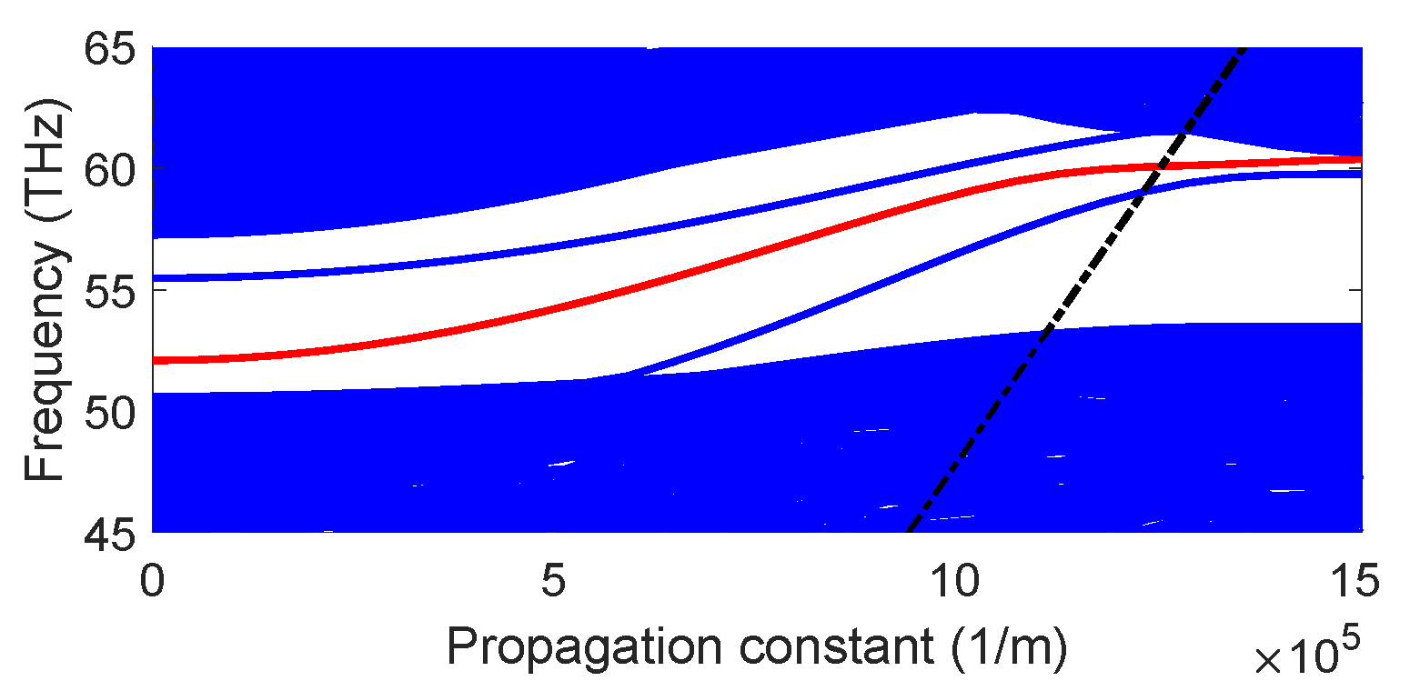
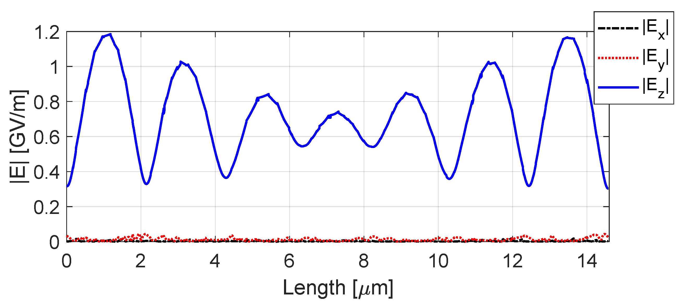
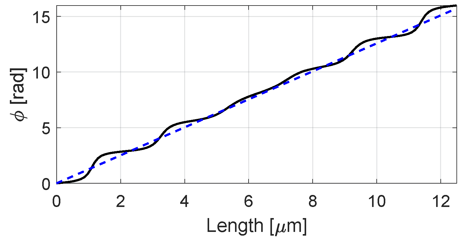
3. Numerical Results
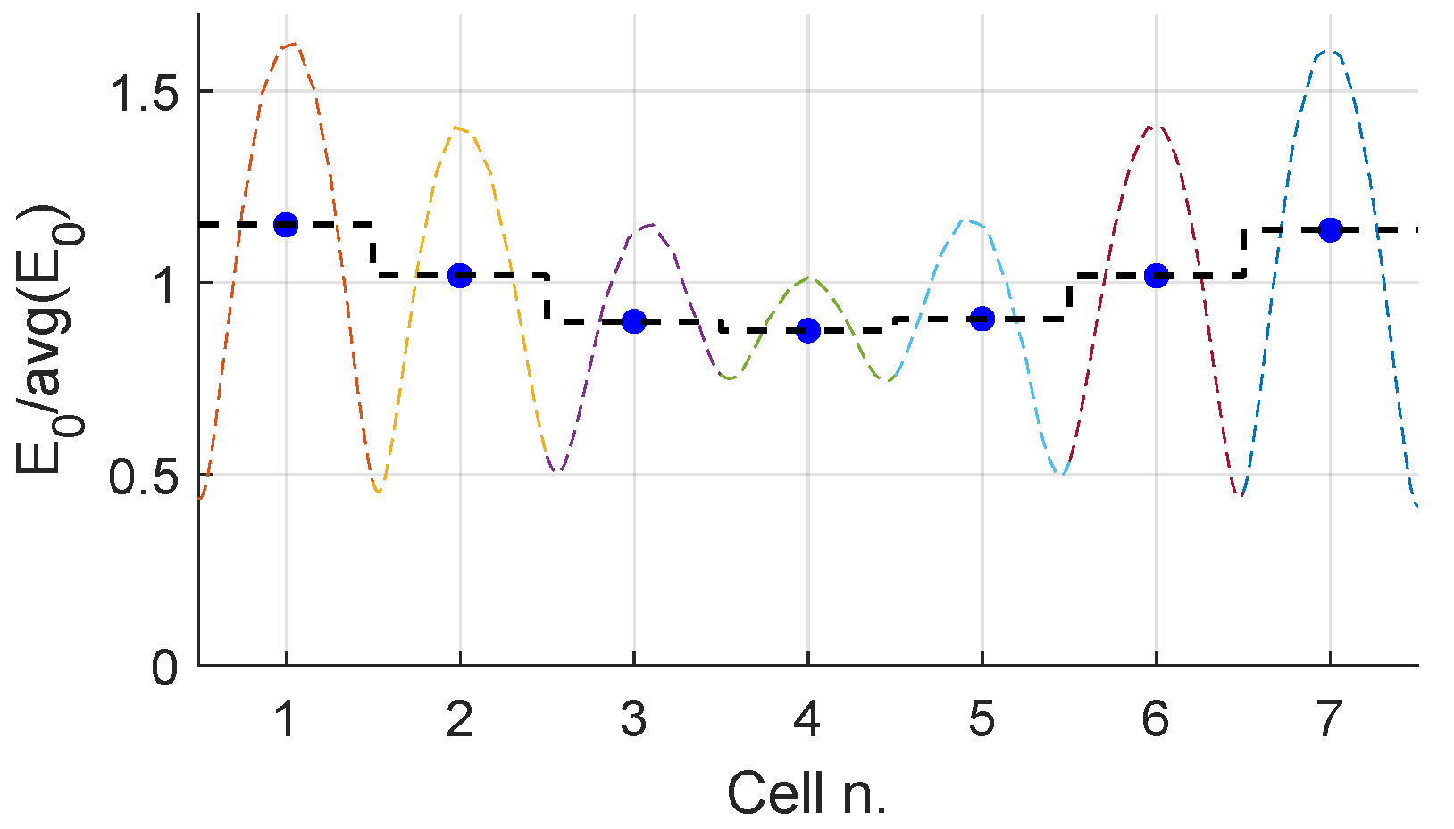
The structure is simulated and tuned by using the commercial software Ansys HFSS [18] and CST Studio Suite [19] with the objective to minimize IL and enhance the overall wave transmission from inputs 1 and 2 to outputs 3 and 4, at the same time optimizing the quality of the TE 10 -to-TM 01 mode conversion. The obtained results are equivalent between the two software packages; therefore, only the HFSS results are reported. Figure 4 shows the S-parameters: the operational bandwidth at I L = 0.5 dB is 60.06–60.08 THz, and the mode conversion is optimal at f 0 = 60.074 THz. Figure 5 shows the electric field components along the accelerating waveguide axis at the frequency of 60.074 THz, for a length of 7 d = 14.574   μ m and input power of 1 kW: it can be seen that the field presents a strong longitudinal component | E z | , while the transversal components, | E x | and | E y | , are almost equal to zero, as in the case of a TM 01 -like mode. Nevertheless, the accelerating field reaches a maximum of ≃1.2 GV/m with an input power of 1 kW, thus confirming that the presented solution meets the required performance needed for future DLAs setups.
Figure 6a shows the electric field vector plot of the accelerating TM 01 -like mode along a x y structure slice at an arbitrary z position along the accelerating waveguide axis. For the same z position, Figure 6b shows the electric field components along the x axis. As expected, on axis ( x = 0 ), the transversal components are almost equal to zero while the longitudinal component has high amplitude. Finally, Figure 7 shows the phase advancement of the TM 01 -like mode along the accelerating hollow-core waveguide at the operating frequency. It is possible to conclude that the phase is suitable to accelerate a speed-of-light particle since its advancement follows the light line.

4. Figures of Merit

Some considerations can be made by analyzing the field components shown in Figure 5a. It is useful to define an average axial electric-field amplitude E 0 = V 0 / L , where V 0 is the RF voltage along the accelerating length, given by V 0 = L / 2 L / 2 E z ( z ) d z , with E z ( z ) being the axial, accelerating electric field and L some characteristic length [20]. Usually, a constant gain per cell is desirable, and the cavity cells are tuned to produce a uniform field distribution along the LINAC; a parameter to evaluate this property is the so-called field flatness. In real scenarios, the field can tilt due to various types of distortions, and these undesirable deviations increase as the total cavity length increases. It is then of interest to evaluate the field flatness in order to quantify the field tilt. The flatness is usually calculated by examining the average electric field along the chain of LINAC cells, which is evaluated cell by cell. In our case, for the field flatness calculation, we can choose the woodpile lattice constant d in place of the cell length. In fact, as clearly seen in Figure 2b, the accelerating channel is composed of several woodpile periods (seven in the case at hand), and each period effectively resembles an accelerating cell with a local electric field. The field flatness for the presented structure results in about ±14% and is shown in Figure 8. The accelerating field flatness requirements depend on the LINAC application and can be improved through several techniques, such as a fine tuning of the coupling section and by a local modification of the single cells transversal dimensions, such as the cell radius for the metallic LINACs that employ cylindrical cavities.
It is useful to make some final calculations to estimate some typical LINAC parameters of merit for the case at hand. The particle energy gain, Δ W , can be expressed in terms of the accelerating gradient, E 0 T , as Δ W = q E 0 L T c o s ϕ ([20] p. 34), where L = 7 d = 14.574   μ m is the accelerating channel length, T is the so-called transit-time factor, defined as
T = L / 2 L / 2 E z ( z ) cos ( ω t ( z ) ϕ ( z ) ϕ 0 ) d z L / 2 L / 2 E z ( z ) d z
and ϕ ( z ) = E z ( z ) is the accelerating field phase. It is usual to fix the phase ϕ = 0 when the particle is at the field crest position so that maximum energy gain occurs when ϕ = 0 , which is often the choice for relativistic electrons. In our case, T = 0.9463 1 , since, as is visible from Figure 7, the phase profile is linear and well matched with the light line, although it has a small unavoidable modulation. In order to have a figure of merit independent from the input power, P 0 , it is common to define the characteristic interaction impedance, which is a measure of the effective accelerating field acting on the electrons E acc = E 0 T , for a given total electromagnetic power, P 0 , flowing into the system ([21] Equation (10) ([22] p. 13):
Z c = ( E 0 T λ ) 2 P 0 [ Ω ]
For the 14.574   μ m long structure presented above, we obtain a characteristic interaction impedance Z c = 11.4 k Ω . For comparison, in [23], a Z c 1 k Ω is obtained in a Bragg waveguide by employing a fictitious material with ϵ r = 25 . With the above accelerating impedance, by taking the average of the electric field along the accelerating channel, E 0 = 0.726 GV/m (see Figure 5), a 14.5 cm long accelerating channel is sufficient to obtain 100 MeV of energy gain Δ W , resulting in an extremely compact structure.

5. Conclusions and Perspectives

In this paper, we present the design of a compact dielectric coupler for future DLA setups, working at the wavelength of 5 μ m and based on a woodpile PhC. The hollow-core structure allows to convert an input TE 10 -like mode, coming from two input waveguides, into a TM 01 -like mode, accelerating the electron bunch injected into the structure with a particle velocity that is synchronous with the phase velocity of the accelerating field. The structure is conceived using advanced photonic concepts, such as the EBG properties of 3D periodic structures, and tuned through the use of commercial simulators, showing very good S-parameter performance inside the operational bandwidth centered at the frequency of 60.074 THz, where an efficient mode conversion is also observed. The presented coupler could represent a crucial component for enabling the realization of future tabletop DLAs.

Author Contributions

Conceptualization, G.S.M., G.T., D.M. and G.S.; methodology, G.S.M., G.T., A.L., C.D.A. and G.S.; Figure of merit calculation G.S.M., A.B. and G.S.; writing—original draft preparation, G.S.M., G.T. and G.S.; writing—review and editing, all authors. All authors have read and agreed to the published version of the manuscript.

Funding

This research received no external funding.

Institutional Review Board Statement

Not applicable.

Informed Consent Statement

Not applicable.

Acknowledgments

This work is supported by INFN V National Committee under the MICRON grant.

Conflicts of Interest

The authors declare no conflict of interest.

References

  1. Engl, R.J.; Noble, R.J.; Bane, K.; Dowell, D.H.; Ng, C.K.; Spencer, J.E.; Tantawi, S.; Wu, Z.; Byer, R.L.; Peralta, E.; et al. Dielectric laser accelerators. Rev. Mod. Phys. 2014, 86, 1337–1389. [Google Scholar]
  2. Niedermayer, U.; Egenolf, T.; Boine-Frankenheim, O. Three Dimensional Alternating-Phase Focusing for Dielectric-Laser Electron Accelerators. Phys. Rev. Lett. 2020, 125, 164801. [Google Scholar] [CrossRef] [PubMed]
  3. Sapra, N.V.; Yang, K.Y.; Vercruysse, D.; Leedle, K.J.; Black, D.S.; England, R.J.; Su, L.; Trivedi, R.; Miao, Y.; Solgaard, O.; et al. On-chip integrated laser-driven particle accelerator. Science 2020, 367, 79–83. [Google Scholar] [CrossRef] [PubMed] [Green Version]
  4. Accelerator on a Chip International Program (ACHIP). Available online: https://achip.stanford.edu/ (accessed on 27 February 2022).
  5. Naranjo, B.; Valloni, A.; Putterman, S.; Rosenzweig, J.B. Stable Charged-Particle Acceleration and Focusing in a Laser Accelerator Using Spatial Harmonics. Phys. Rev. Lett. 2012, 109, 164803. [Google Scholar] [CrossRef] [PubMed]
  6. Joannopoulos, J.D.; Johnson, S.G.; Winn, J.N.; Meade, R.D. Photonic Crystals: Molding the Flow of Light, 2nd ed.; Princeton University Press: Princeton, NJ, USA, 2011. [Google Scholar]
  7. Hermatschweiler, M.; Ledermann, A.; Ozin, G.A.; Wegener, M.; von Freymann, G. Fabrication of silicon inverse woodpile photonic crystals. Adv. Funct. Mater. 2007, 17, 2273–2277. [Google Scholar] [CrossRef] [Green Version]
  8. Staude, I.; McGuinness, C.; Frölich, A.; Byer, R.L.; Colby, E.; Wegener, M. Waveguides in three-dimensional photonic bandgap materials for particle-accelerator on a chip architectures. Opt. Express 2012, 20, 5607–5612. [Google Scholar] [CrossRef] [PubMed]
  9. Wu, Z.; England, R.J.; Ng, C.K.; Cowan, B.; McGuinness, C.; Lee, C.; Qi, M.; Tantawi, S. Coupling power into accelerating mode of a three-dimensional silicon woodpile photonic band-gap waveguide. Phys. Rev. ST Accel. Beams 2014, 17, 081301. [Google Scholar] [CrossRef] [Green Version]
  10. Mauro, G.; Torrisi, G.; Mascali, D.; Sorbello, G.; Bacci, A.; Rossi, A.; De Angelis, C.; Locatelli, A. Numerical Simulation and Beam-Dynamics Study of a Hollow-Core Woodpile Coupler for Dielectric Laser Accelerators. In Proceedings of the 12th International Particle Accelerator Conference (IPAC’21), Campinas, Brazil, 24–28 May 2021; JACOW Publishing: Geneva, Switzerland, 2021; pp. 2022–2025. [Google Scholar] [CrossRef]
  11. Zhao, X.; Yuan, C.; Zhang, Q.; Zhao, L. Design and experiment study of compact circular-rectangular waveguide mode converter. Rev. Sci. Instrum. 2016, 87, 074707. [Google Scholar] [CrossRef] [PubMed]
  12. Alesini, D.; Citterio, A.; Campogiani, G.; Ficcadenti, L.; Migliorati, M.; Mostacci, A.; Palumbo, L.; Persichelli, S.; Zennaro, R. Tuning procedure for traveling wave structures and its application to the C-Band cavities for SPARC photo injector energy upgrade. J. Instrum. 2013, 8, P10010. [Google Scholar] [CrossRef]
  13. Johnson, S.G. MIT Photonics-Bands (MPB). Available online: http://ab-initio.mit.edu/photons/tutorial/ (accessed on 27 February 2022).
  14. Mauro, G.S.; Locatelli, A.; Torrisi, G.; Leonardi, O.; Celona, L.; De Angelis, C.; Sorbello, G. Fabrication and Characterization of Woodpile Waveguides for Microwave Injection in Ion Sources. IEEE Trans. Microw. Theory Tech. 2020, 68, 1621–1626. [Google Scholar] [CrossRef]
  15. Torrisi, G.; Locatelli, A.; Mauro, G.S.; Bellettato, M.; Celona, L.; Mancarella, F.; De Angelis, C.; Sorbello, G. Design and Characterization of a Silicon W-Band Woodpile Photonic Crystal Waveguide. IEEE Microw. Wirel. Compon. Lett. 2020, 30, 347–350. [Google Scholar] [CrossRef]
  16. Siemann, R. Energy efficiency of laser driven, structure based accelerators. Phys. Rev. Spec.-Top.-Accel. Beams 2004, 7, 061303. [Google Scholar] [CrossRef] [Green Version]
  17. Na, Y.N.; Siemann, R.; Byer, R. Energy efficiency of an intracavity coupled, laser-driven linear accelerator pumped by an external laser. Phys. Rev. Spec.-Top.-Accel. Beams 2005, 8, 031301. [Google Scholar] [CrossRef] [Green Version]
  18. Ansys HFSS; Ansoft Corp.: Pittsburgh, PA, USA, 2021.
  19. CST Microwave Studio. Dassault Systèmes; Vélizy-Villacoublay: Paris, France, 2021. [Google Scholar]
  20. Wangler, T.P. RF Linear Accelerators; Wiley-VCH, Verlag GmbH & Co. KGaA: Weinheim, Germany, 2008. [Google Scholar]
  21. Aloisio, M.; Sorbello, G. One-Third-of-Pitch Reduction Technique for the Analysis of Ternary Azimuthally Periodic Helical Slow-wave Structures. IEEE Trans. Electron Devices 2006, 53, 1467–1473. [Google Scholar] [CrossRef]
  22. Schachter, L.; Wilson, P.B. Beam-Wave Interaction in Periodic and Quasi-Periodic Structures. Physics Today 1998, 51, 90. [Google Scholar] [CrossRef]
  23. Mizrahi, A.; Schächter, L. Optical Bragg accelerators. Phys. Rev. E 2004, 70, 016505. [Google Scholar] [CrossRef] [PubMed] [Green Version]
Figure 1. 3D model of the presented EBG woodpile coupler. One input (1) and one output (3) TE 10 -like mode hollow-core waveguides are highlighted with red dashed lines.
Applsci 12 02609 g001
Figure 2. (a) Accelerating waveguide front view with fundamental geometrical parameters w, h, d and hollow-core defect dimensions w d , h d . (b) Structure slice in the x z plane. It is composed of two mode converters (from TE 10 -like to TM 01 -like mode and vice versa) and an accelerating waveguide. One of the two bricks composing the short wall of the exit mode converter is also highlighted by a green circle.
Applsci 12 02609 g002
Figure 3. Projected band diagram of the isolated accelerating waveguide along the axis (z axis). The diagram shows a band-gap (white-colored) extending from 50 to 60 THz, depending on the value of the propagation constant. The lines running through the band-gap are guided modes introduced by the longitudinal defect. In particular, the red line is a TM 01 -like mode, with an axial component suitable for particle acceleration. The light line (black dash-dotted curve) intercepts the guided TM 01 -like mode at the frequency of 60.057 THz: this synchronous point is chosen as a working point to obtain the acceleration of relativistic electrons.
Applsci 12 02609 g003
Figure 4. | S b a | and | S a a | for the presented EBG woodpile coupler, where a = 1 + 2 and b = 3 + 4 . See Figure 2b for I/O ports numbering.
Applsci 12 02609 g004
Figure 5. Electric field components along the accelerating waveguide axis at f 0 = 60.074 THz, for a length of 7 d = 14.574 μ m. The average field, obtained with an input power P 0 = 1 kW, results in E 0 = 0.726 GV/m.
Applsci 12 02609 g005
Figure 6. (a) Electric field vector plot of the accelerating TM 01 -like mode along a x y structure slice for an arbitrarily chosen z position. (b) Electric field components along the x axis (blue dashed horizontal line of a) for the same z position, at f 0 = 60.074 THz and with P 0 = 1 kW. Green dashed vertical lines indicate the defect width, w d .
Applsci 12 02609 g006
Figure 7. Black line: phase of the longitudinal (accelerating) component, E z , vs z. Blue dashed line: light line of a relativistic particle. The operating frequency is f 0 = 60.074 THz. It can be seen that the phase advancement along the structure is compatible with a particle moving at speed of light: a relativistic particle “sees” a constant phase while traveling along the structure.
Applsci 12 02609 g007
Figure 8. Electric field flatness plot vs. cell (period) number. Blue-filled dots indicate the cell-by-cell average electric field value E 0 divided by the average of all E 0 values for the seven cells. Black dashed lines indicate, for each cell, the length on which the average value is taken. For the presented structure, the flatness is about ±14%.
Applsci 12 02609 g008
Publisher’s Note: MDPI stays neutral with regard to jurisdictional claims in published maps and institutional affiliations.

