
Atomic-Layer-Deposition-Made Very Thin Layer of Al2O3, Improves the Young’s Modulus of Graphene


Abstract
:
1. Introduction
2. Materials and Methods
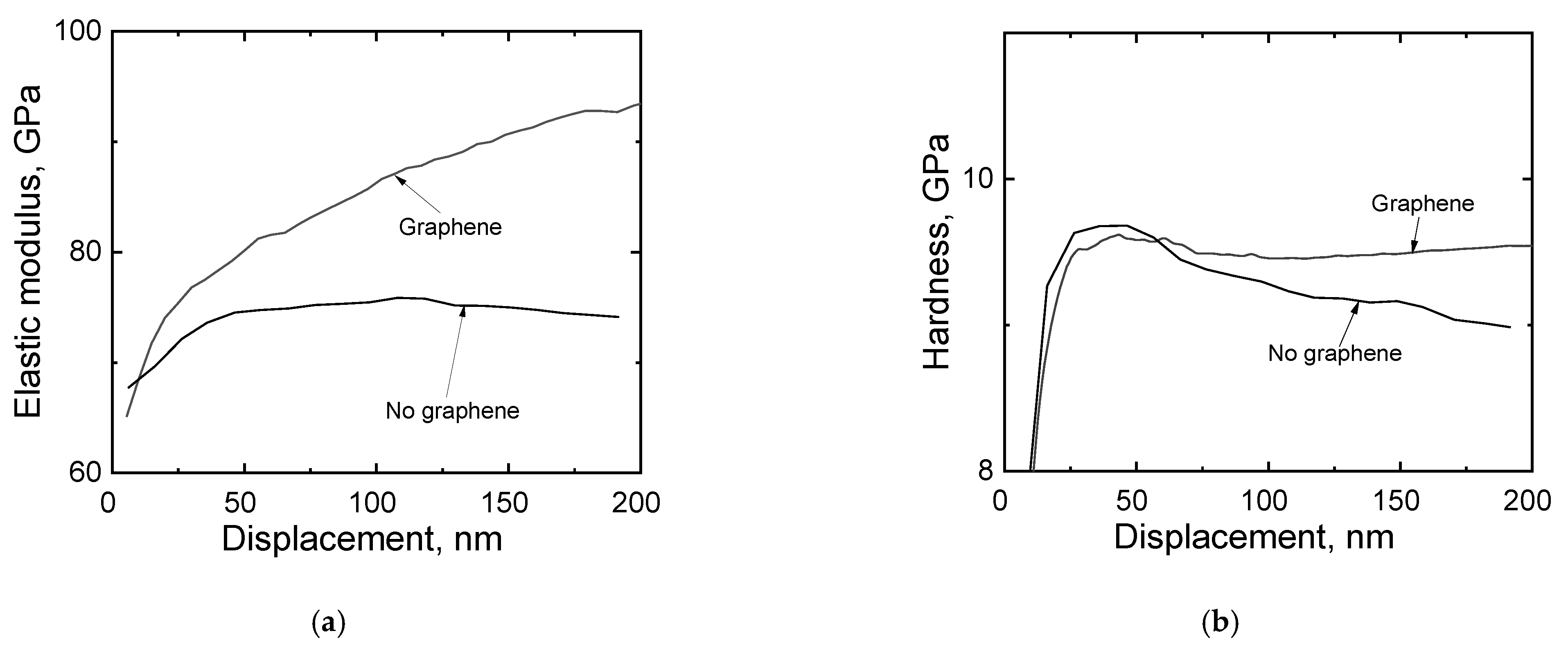
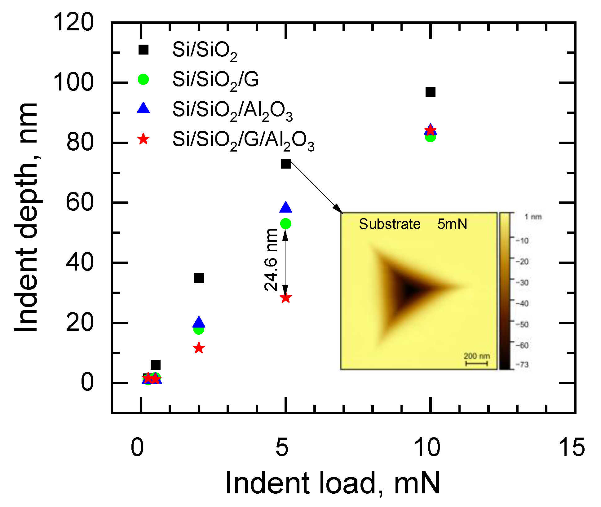
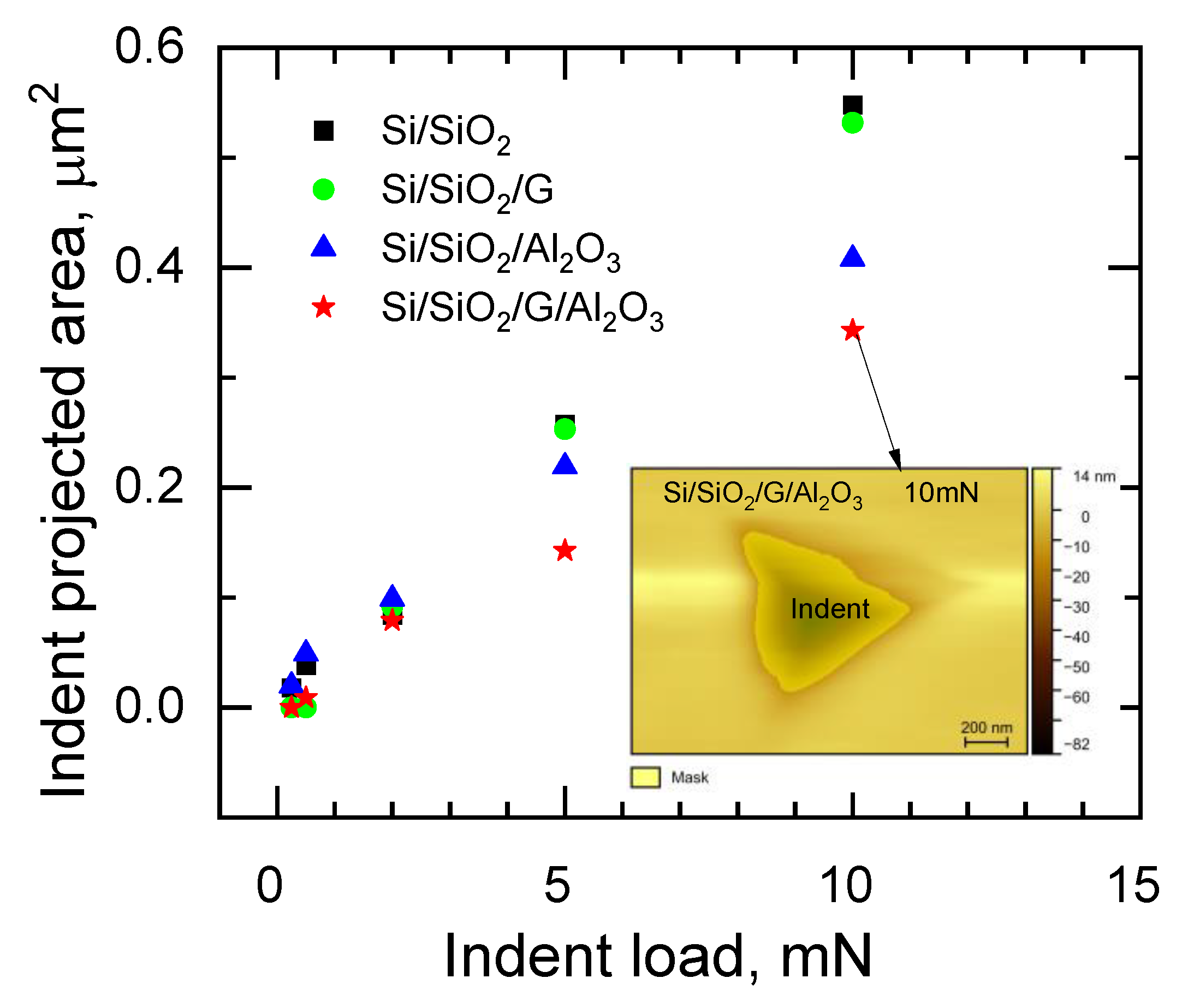
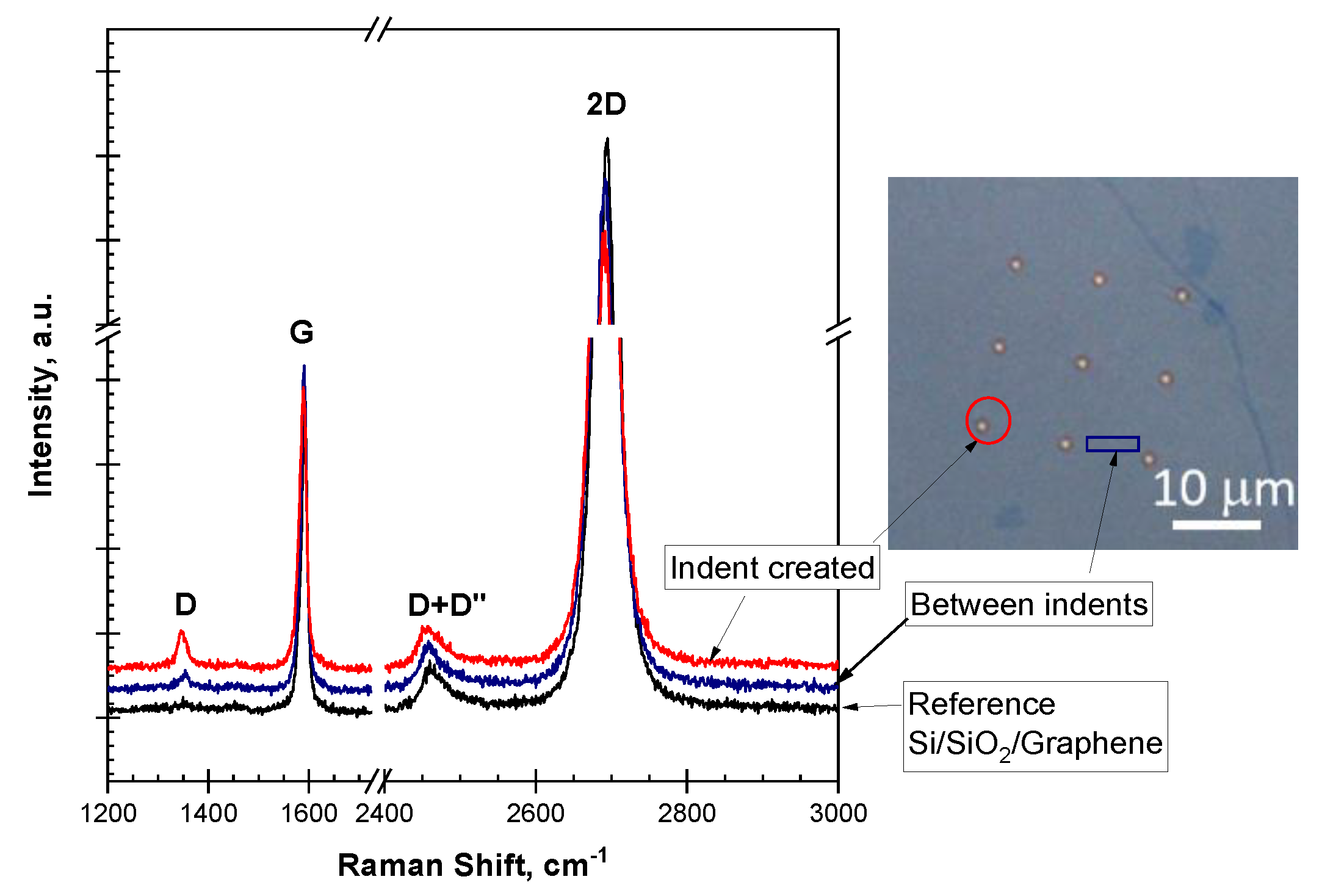
3. Results
4. Discussion
5. Conclusions
Author Contributions
Funding
Institutional Review Board Statement
Informed Consent Statement
Data Availability Statement
Acknowledgments
Conflicts of Interest
References
- Ali, M.M.; Mitchell, J.J.; Burwell, G.; Rejnhard, K.; Jenkins, C.A.; Ahmadi, E.D.; Sharma, S.; Guy, O.J. Application of Molecular Vapour Deposited Al2O3 for Graphene-Based Biosensor Passivation and Improvements in Graphene Device Homogeneity. Nanomaterials 2021, 11, 2121. [Google Scholar] [CrossRef]
- Hassani, N.; Rashidi, R.; Miloševic, M.V.; Neek-Amal, M. Evaluating gas permeance through graphene nanopores and porous 2D-membranes: A generalized approach. Carbon Trends 2021, 5, 100086. [Google Scholar] [CrossRef]
- Kodu, M.; Berholts, A.; Kahro, T.; Eriksson, J.; Yakimova, R.; Avarmaa, T.; Renge, I.; Alles, H.; Jaaniso, R. Graphene-Based Ammonia Sensors Functionalised with Sub-Monolayer V2O5: A Comparative Study of Chemical Vapour Deposited and Epitaxial Graphene. Sensors 2019, 19, 951. [Google Scholar] [CrossRef] [PubMed] [Green Version]
- Son, I.H.; Park, J.H.; Park, S.; Park, K.; Han, S.; Shin, J.; Doo, S.-G.; Hwang, Y.; Chang, H.; Choi, J.W. Graphene balls for lithium rechargeable batteries with fast charging and high volumetric energy densities. Nat. Commun. 2017, 8, 1561. [Google Scholar] [CrossRef] [PubMed]
- Hussain, S.; Kongi, N.; Treshchalov, A.; Kahro, T.; Rähn, M.; Merisalu, M.; Tamm, A.; Sammelselg, V.; Tammeveski, K. Enhanced oxygen reduction reaction activity and durability of Pt nanoparticles deposited on graphene-coated alumina nanofibres. Nanoscale Adv. 2021, 3, 2261–2268. [Google Scholar] [CrossRef]
- Xia, F.; Farmer, D.B.; Lin, Y.-M.; Avouris, P. Graphene Field-Effect Transistors with High On/Off Current Ratio and Large Transport Band Gap at Room Temperature. Nano Lett. 2010, 10, 715–718. [Google Scholar] [CrossRef] [Green Version]
- Kahro, T.; Tarre, A.; Käämbre, T.; Piirsoo, H.-M.; Kozlova, J.; Ritslaid, P.; Kasikov, A.; Jõgiaas, T.; Vinuesa, G.; Dueñas, S.; et al. Hafnium Oxide/Graphene/Hafnium Oxide-Stacked Nanostructures as Resistive Switching Media. CS Appl. Nano Mater. 2021, 4, 5152–5163. [Google Scholar] [CrossRef]
- Kahro, T.; Castán, H.; Dueñas, S.; Merisalu, J.; Kozlova, J.; Jõgiaas, T.; Piirsoo, H.-M.; Kasikov, A.; Ritslaid, P.; Mändar, H.; et al. Structure and behavior of ZrO2-graphene-ZrO2 stacks. J. Vac. Sci. Technol. A 2020, 38, 063411. [Google Scholar] [CrossRef]
- Qiu, X.P.; Shin, Y.J.; Niu, J.; Kulothungasagaran, N.; Kalon, G.; Qiu, C.; Yu, T.; Yang, H. Disorder-free sputtering method on graphene. AIP Adv. 2012, 2, 032121. [Google Scholar] [CrossRef]
- Vervuurt, R.H.J.; Kessels, W.M.M.; Bol, A. Atomic Layer Deposition for Graphene Device Integration. Adv. Mater. Interfaces 2017, 4, 1700232. [Google Scholar] [CrossRef] [Green Version]
- Tamm, A.; Kozlova, J.; Aarik, L.; Aidla, A.; Lu, J.; Kiisler, A.-A.; Kasikov, A.; Ritslaid, P.; Mändar, H.; Hultman, L.; et al. Atomic layer deposition of ZrO2 for graphene-based multilayer structures: In situ and ex situ characterization of growth process. Phys. Status Solidi A 2013, 211, 397–402. [Google Scholar] [CrossRef]
- Jõgiaas, T.; Tarre, A.; Mändar, H.; Kozlova, J.; Tamm, A. Nanoindentation of Chromium Oxide Possessing Superior Hardness among Atomic-Layer-Deposited Oxides. Nanomaterials 2022, 12, 82. [Google Scholar] [CrossRef] [PubMed]
- Zhang, Y.; Pan, C. Measurements of mechanical properties and number of layers of graphene from nano-indentation. Diam. Relat. Mater. 2012, 24, 1–5. [Google Scholar] [CrossRef]
- Daniels, C.; Horning, A.; Phillips, A.; Massote, D.V.P.; Liang, L.; Bullard, Z.; Sumpter, B.G.; Meunier, V. Elastic, plastic, and fracture mechanisms in graphene materials. J. Phys. Condens. Matter 2015, 27, 373002. [Google Scholar] [CrossRef]
- Rabiei, M.; Palevicius, A.; Dashti, A.; Nasiri, S.; Monshi, A.; Vilkauskas, A.; Janusas, G. Measurement Modulus of Elasticity Related to the Atomic Density of Planes in Unit Cell of Crystal Lattices. Materials 2020, 13, 4380. [Google Scholar] [CrossRef]
- Rabiei, M.; Palevicius, A.; Nasiri, S.; Dashti, A.; Vilkauskas, A.; Janusas, G. Relationship between Young’s Modulus and Planar Density of Unit Cell, Super Cells (2 × 2 × 2), Symmetry Cells of Perovskite (CaTiO3). Lattice Mater. 2021, 14, 1258. [Google Scholar] [CrossRef]
- Rezaei, R. Tensile mechanical characteristics and deformation mechanism of metal-graphene nanolayered composites. Comput. Mat. Sci. 2018, 151, 181–188. [Google Scholar] [CrossRef]
- Fan, Y.-C.; Wu, C.-D.; Fang, T.-H.; Chen, T.-H. Thermal relaxation and deformation of indented graphene. Comput. Mat. Sci. 2013, 79, 105–109. [Google Scholar] [CrossRef]
- Tan, X.; Wu, J.; Zhang, K.; Peng, X.; Sun, L.; Zhong, J. Nanoindentation models and Young’s modulus of monolayer graphene: A molecular dynamics study. Appl. Phys. Lett. 2013, 102, 071908. [Google Scholar] [CrossRef]
- Beams, R.; Cançado, L.G.; Novotny, L. Raman characterization of defects and dopants in graphene. J. Phys. Condens. Matter 2015, 27, 083002. [Google Scholar] [CrossRef]
- Ferrari, A.C.; Basko, D.M. Raman spectroscopy as a versatile tool for studying the properties of graphene. Nat. Nanotechnol. 2013, 8, 235–246. [Google Scholar] [CrossRef] [PubMed] [Green Version]
- Wang, Q.H.; Jin, Z.; Kim, K.K.; Hilmer, A.J.; Paulus, G.L.C.; Shih, C.-J.; Ham, M.-H.; Sanchez-Yamagishi, J.D.; Watanabe, K.; Taniguchi, T.; et al. Understanding and controlling the substrate effect on graphene electron-transfer chemistry via reactivity imprint lithography. Nat. Chem. 2012, 4, 724–732. [Google Scholar] [CrossRef] [PubMed]
- Neumann, C.; Reichardt, S.; Venezuela, P.; Drögeler, M.; Banszerus, L.; Schmitz, M.; Watanabe, K.; Taniguchi, T.; Mauri, F.; Beschoten, B.; et al. Raman spectroscopy as probe of nanometre-scale strain variations in graphene. Nat. Commun. 2015, 6, 8429. [Google Scholar] [CrossRef] [PubMed] [Green Version]
- Maad, B.; Durnez, A.; ·Ajlani, H.; Madouri, A.; Oueslati, M.; ·Meftah, A. Modulation of electron transfer in Si/SiO2/HfO2/Graphene by the HfO2 thickness. Appl. Phys. A 2020, 126, 754. [Google Scholar] [CrossRef]
- Sha, Z.D.; Wan, Q.; Pei, Q.X.; Quek, S.S.; Liu, Z.S.; Zhang, Y.W.; Shenoy, V.B. On the failure load and mechanism of polycrystalline graphene by nanoindentation. Sci. Rep. 2014, 4, 7437. [Google Scholar] [CrossRef] [PubMed] [Green Version]
- Lee, G.-H.; Cooper, R.C.; An, S.J.; Lee, S.; van der Zande, A.; Petrone, N.; Hammerberg, A.G.; Lee, C.; Crawford, B.; Oliver, W.; et al. High-Strength Chemical-Vapor–Deposited Graphene and Grain Boundaries. Science 2013, 340, 1073–1076. [Google Scholar] [CrossRef]
- Hobi, E.; Pontes, R.B., Jr.; Fazzio, A.; da Silva, A.J.R. Formation of atomic carbon chains from graphene nanoribbons. Phys. Rev. B 2010, 81, 201406. [Google Scholar] [CrossRef] [Green Version]
- Peikolainen, A.-L.; Uibu, M.; Kozlova, J.; Mändar, H.; Tamm, A.; Aablo, A. Carbon xerogel from 5-methylresorcinol-formaldehyde gel: The controllability of structural properties. Carbon Trends 2021, 3, 100037. [Google Scholar] [CrossRef]
- Tamm, A.; Piirsoo, H.-M.; Jõgiaas, T.; Tarre, T.; Link, J.; Stern, R.; Kukli, K. Mechanical and Magnetic Properties of Double Layered Nanostructures of Tin and Zirconium Oxides Grown by Atomic Layer Deposition. Nanomaterials 2021, 11, 1633. [Google Scholar] [CrossRef]


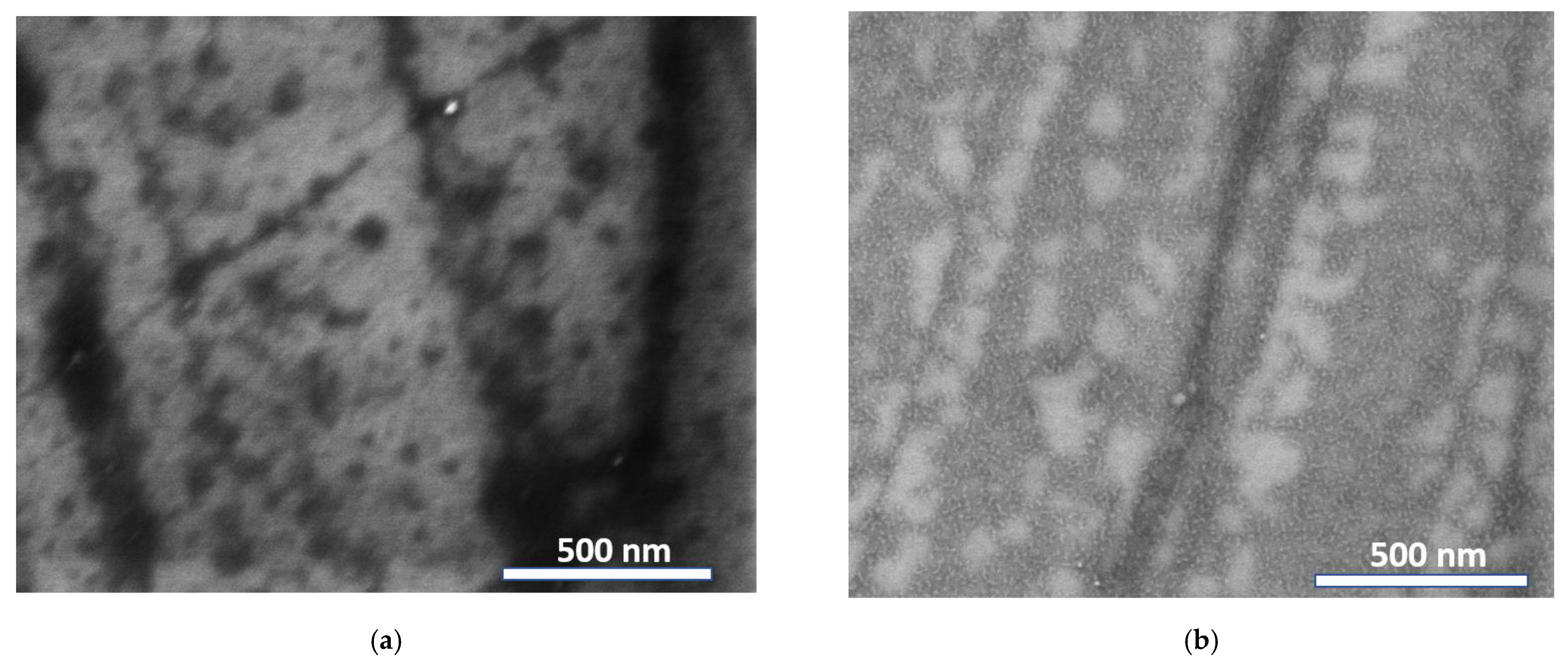
| EDX Spectrum | C | O | Al | Si |
|---|---|---|---|---|
| Si/SiO2/G | 1.69 | 33.19 | 0.0 | 65.12 |
| Si/SiO2/G/Al2O3 | 1.05 | 55.96 | 0.49 | 42.50 |
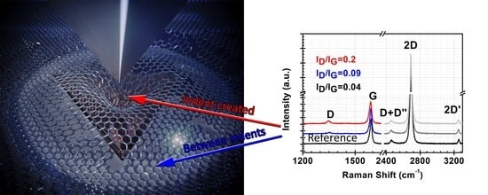
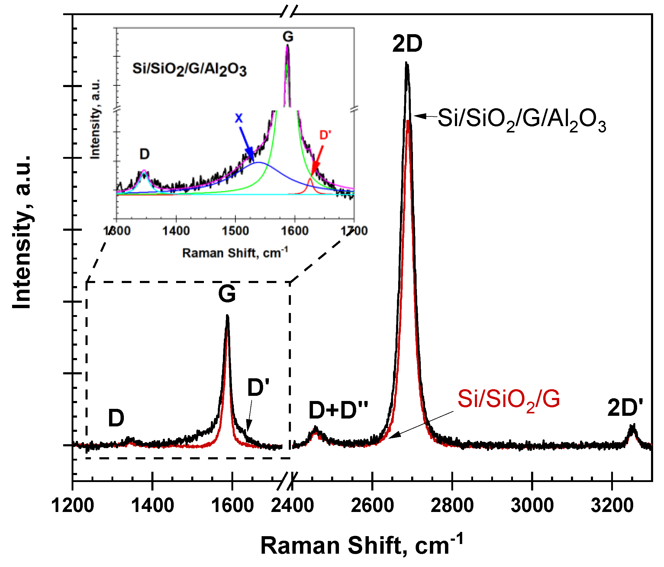
| Sample | ωG (cm−1) | ΓG (cm−1) | ω2D (cm−1) | Γ2D (cm−1) | ID/IG |
|---|---|---|---|---|---|
| Si/SiO2/G | 1588.5 | 15.5 | 2690.0 | 34.0 | 0.04 |
| Si/SiO2/G/Al2O3 | 1587.5 | 18.0 | 2689.5 | 37.5 | 0.05 |
| Ref, Si/SiO2/G/Al2O3 | 1594 | 32 | 2707 | 62 | 1.3 |
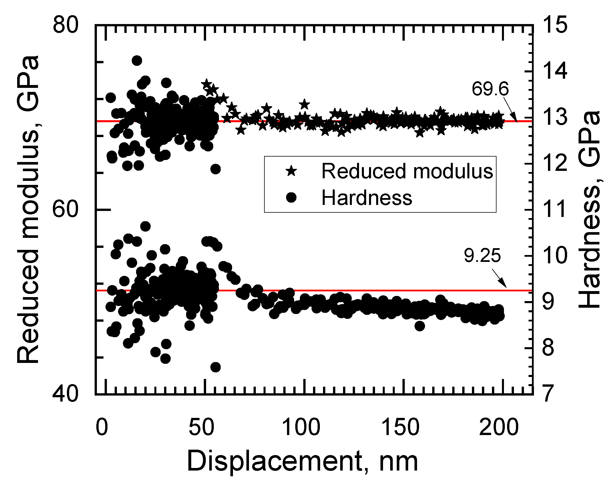
| Sample | Max. Load (mN) | D-Band Area Measured on Hole | D-Band Area between Holes | Max. Ave. Young’s Modulus (Gpa) |
|---|---|---|---|---|
| Si/SiO2/G | 10 | 12,366 | 6578.5 | 96.0 |
| 5.0 | 5825 | 1767 | 93 | |
| 2.0 | 5653 | 2514 | 88 | |
| 0.5 | 5425 | 3006 | 80 | |
| Si/SiO2/G/Al2O3 | 10 | 6220 | 3967 | 125 |
| 5 | 5566 | 3967 | 107 | |
| 2 | 6529 | 1568 | 95 |
Publisher’s Note: MDPI stays neutral with regard to jurisdictional claims in published maps and institutional affiliations. |
© 2022 by the authors. Licensee MDPI, Basel, Switzerland. This article is an open access article distributed under the terms and conditions of the Creative Commons Attribution (CC BY) license (https://creativecommons.org/licenses/by/4.0/).
Share and Cite
Tamm, A.; Kahro, T.; Piirsoo, H.-M.; Jõgiaas, T. Atomic-Layer-Deposition-Made Very Thin Layer of Al2O3, Improves the Young’s Modulus of Graphene. Appl. Sci. 2022, 12, 2491. https://doi.org/10.3390/app12052491
Tamm A, Kahro T, Piirsoo H-M, Jõgiaas T. Atomic-Layer-Deposition-Made Very Thin Layer of Al2O3, Improves the Young’s Modulus of Graphene. Applied Sciences. 2022; 12(5):2491. https://doi.org/10.3390/app12052491
Chicago/Turabian StyleTamm, Aile, Tauno Kahro, Helle-Mai Piirsoo, and Taivo Jõgiaas. 2022. "Atomic-Layer-Deposition-Made Very Thin Layer of Al2O3, Improves the Young’s Modulus of Graphene" Applied Sciences 12, no. 5: 2491. https://doi.org/10.3390/app12052491
APA StyleTamm, A., Kahro, T., Piirsoo, H.-M., & Jõgiaas, T. (2022). Atomic-Layer-Deposition-Made Very Thin Layer of Al2O3, Improves the Young’s Modulus of Graphene. Applied Sciences, 12(5), 2491. https://doi.org/10.3390/app12052491