1. Introduction
With the characteristics of being environmentally friendly and reducing fuel consumption, electric vehicles (EVs) are becoming popular. The chargers of EVs can be categorized into two classes—slow charging and fast charging. The fast chargers are usually installed in highway rest areas and city refueling points [
1]. The slow chargers are usually installed in community parking sites or located on-board. Usually, these chargers include an AC/DC converter followed by a second-stage DC/DC converter [
2] or one-stage DC/DC converter powered by a high-voltage DC bus [
3]. Some AC/DC converters can be used to charge the EVs directly. However, the control is complex [
4]. Usually, DC/DC converters are used in chargers and the input voltage of these DC/DC converters is high. To reduce the voltage stress, the DC/DC converter can be implemented by an isolated three-level DC/DC converter (ITLDC) [
5,
6]. A four-switch ITLDC was proposed in [
7], which has the simplest structure. Many research works focusing on the four-switch ITLDC have been conducted to achieve high efficiency and reliability. To ensure the reliability of the ITLDC, the voltages of the input capacitors and the current of switches should be balanced. The pulse wide modulation methods are proposed in [
8,
9] to achieve perfect voltage balancing results. The periodically swapping modulation strategy is proposed in [
10] to achieve balanced switch currents. To achieve high efficiency in an ITLDC, soft switching should be realized. This paper will focus on the zero-voltage switching (ZVS) of the four-switch ITLDC.
There are many research works focusing on the ZVS of the diode clamping ITLDC. For example, in [
11,
12], the ZVS is realized with a large load range and reduced circulating loss; in [
13,
14], the ZVZCS methods are proposed, and some switches realize zero-current turn-on and other switches realize zero-voltage turn-on. However, the research works focusing on the ZVS of the four-switch ITLDC are relatively few and these research works are as follows. The ITLDC will achieve natural ZVS with a high output current and the natural ZVS range can be extended by increasing the leakage inductance of the transformer or adding an external inductor in series with the primary winding of the transformer [
11]. However, a too large leakage inductance will result in high duty cycle loss and high circulating loss [
11,
15]. In [
16], a combined DC/DC converter is proposed to realize wide load range ZVS, two ITLDCs’ parallel operation and share two switches of the down bridge; thus, the current stress of the down bridge switches will be high. A wide load range ZVZCS ITLDC with two main switches realized ZVS and another two main switches realized zero-current switching (ZCS) in [
17]. However, when the ITLDC is implemented with MOSFETs, the switching losses will not be substantially reduced with ZCS, due to the large output capacitance of MOSFETs. In [
6], a zero-voltage switching PWM strategy with capacitor current-balancing control is proposed; the ZVS achievement conditions of the upper bridge switches and the down bridge switches are shifted towards each other in every two switching periods; thus, the switching losses caused by the hard switching at the light load situation can be distributed evenly among the four power switches. However, the soft switching range is not extended with this ZVS method. In [
18], a ZVS non-isolated bidirectional DC/DC converter with transient current build-up technique is proposed with a small average auxiliary current, which can be used in ITLDC to realize full load range ZVS. However, this ZVS method needs two auxiliary switches for each bridge and the auxiliary switches are turned off under hard switching conditions.
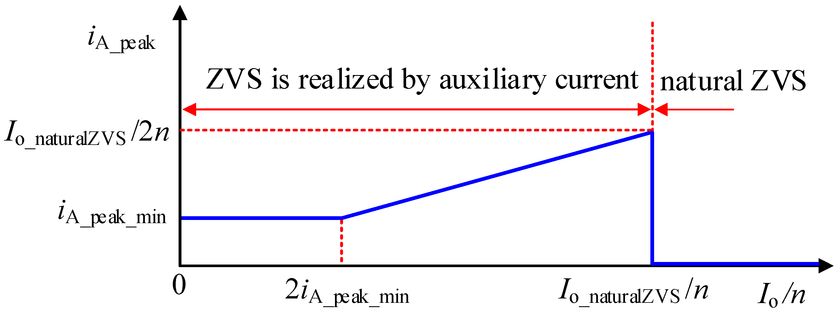
To extend the ZVS range of the ITLDC, a commutation auxiliary circuit (CAC) can be added. A CAC with one inductance and two capacitances is proposed in [
19]. The CAC can be used in different ITLDCs, and also in the four-switch ITLDC, as shown in
Figure 1a. However, this CAC will not perform well when the ITLDC is used as an EV charger. According to [
20,
21], the constant-current and constant-voltage charging strategy is used to charge lithium-ion batteries. In the first charging stage, the batteries are charged with a constant current and, then, the charging process will switch to a constant-voltage stage. During the constant-current stage, the duty cycle of the ITLDC will increase with the increase in battery voltage. During the constant-voltage stage, the output current of the ITLDC will decrease with the charging process time. The maximum value of the auxiliary current
iA is
iA_peak, which will change with the duty cycle. The maximum value
iA_peak can be expressed as (1) [
17] and the change in
iA_peak with duty cycle is shown in
Figure 1b.
where
D is the duty,
Ts is the period,
Vin is the input voltage, and
LA is the auxiliary inductor of the CAC.
As shown in
Figure 1b, to achieve ZVS at a small duty cycle, the auxiliary inductor
LA should be designed with a small value. However, the auxiliary current will be large when the duty cycle is large. The auxiliary current will result in high conduction losses and high current stress of the main switches. Moreover, during the constant-current charging stage, the output current is large enough to realize ZVS naturally, and then the CAC is unwanted. A controllable CAC is required to generate a controllable commutation auxiliary current, which does not change with the duty cycle and can be controlled to zero when the ITLDC realizes ZVS naturally.
This paper proposes an active commutation auxiliary circuit (ACAC) with controllable commutation auxiliary current, which will realize a full load range ZVS of the ITLDC. The ACACs can be left unused when the ITLDC realizes natural ZVS, which will result in high efficiency. Since the ACACs will not work when the current of the ITLDC is large enough to realize natural ZVS, the ACACs do not increase the current stress of the main switches. The auxiliary switch achieves zero-current turn-on and zero-voltage turn-off and the switching loss of the auxiliary switch is quite small. The structure and operating principle of the ITLDC with ACACs are introduced and the performance of the proposed ITLDC is experimentally verified on a 1.5 kW prototype converter.
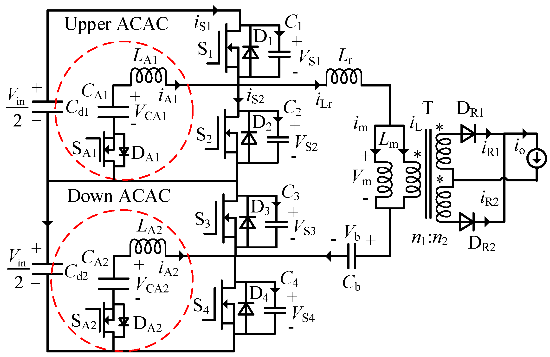
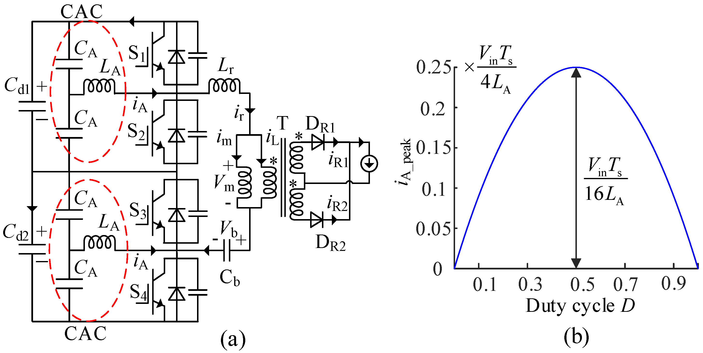
2. Proposed Topology and Working Principle
The topology of the proposed ITLDC is shown in
Figure 2. The ACAC consists of a small auxiliary inductor
LA, an auxiliary capacitor
CA and an auxiliary switch
SA. Two ACACs are applied to the ITLDC’s upper bridge and down bridge, respectively. The auxiliary capacitor
CA is large enough so that the voltage of
CA remains unchanged in one period.
Lr is the leakage inductance of the transformer and
Cb is the DC-blocking capacitor, which is large enough to act as a DC voltage source.
C1~
C4 are the equivalent parallel capacitors, which will achieve a quasi-zero-voltage turn-off condition for the main switches.
VS1~
VS4 are the drain source voltages of the main switches S
1~S
4. The main switches S
1, S
2 are driven by a complementary PWM with dead time and S
3, S
4 are also driven by a complementary PWM with dead time. The PWM phases of S
1 and S
3 are shifted by π degrees.
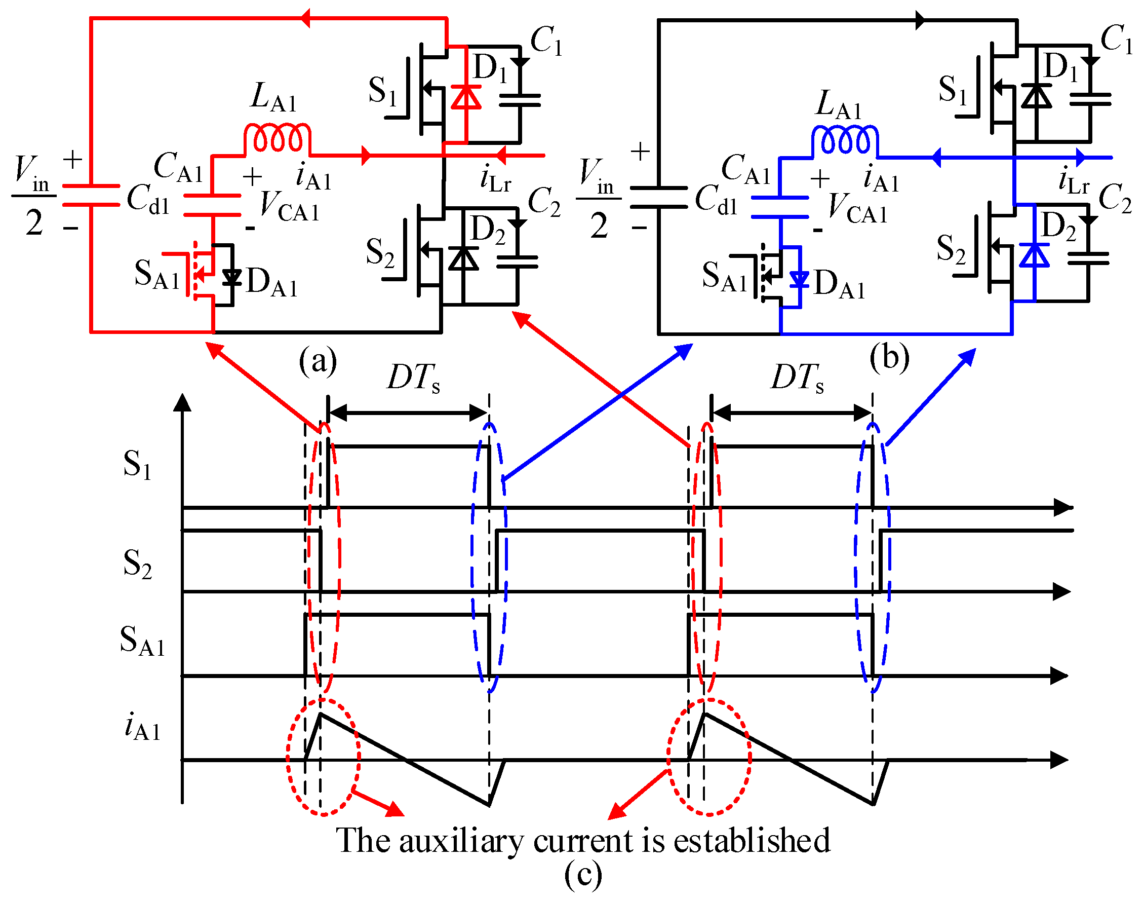
The operating principle and auxiliary current of the upper ACAC are shown in
Figure 3 and the operating principle of the down ACAC is the same as the upper one. Before the switch S
2 is turned off, the auxiliary switch S
A1 is turned on, the voltage
VCA1 is applied to
LA1 and the current
iA1 will increase linearly from zero. The auxiliary switch S
A1 is turned on at the zero-current condition. The auxiliary current
iA1 can be expressed as in (2).
where
VCA1 is the voltage of the auxiliary capacitor
CA1, and
LA1 is the auxiliary inductance.
The current
iA1 will increase linearly until the main switch S
2 is turned off. When S
2 is turned off, the auxiliary current
iA1 increases to
iA_peak, which will be used to achieve the ZVS turn-on of S
1. The auxiliary current
iA1 will discharge the equivalent parallel capacitor
C1 and charge
C2. Once the voltage of
C1 decreases to zero, the antiparallel freewheeling diode D
1 is conducted and the zero-voltage turn-on condition of S
1 is ready, as shown in
Figure 3a. The energy to realize ZVS is taken from
LA1 and
CA1, which are large enough to maintain the zero-voltage condition throughout the entire dead time. After S
1 is turned on at zero-voltage condition, the current
iA1 will decrease linearly, which can be expressed as (3). The current
iA1 will decrease to negative until S
1 is turned off. When S
1 is turned off, the switch S
A1 is also turned off. The negative current of
iA1 will flow through the antiparallel freewheeling diode D
A1 and the auxiliary switch S
A1 is turned off at zero-voltage condition. The negative current of
iA1 will discharge the equivalent parallel capacitor
C2 and charge
C1. Once the voltage of
C2 decreases to zero, the antiparallel freewheeling diode D
2 is conducted and the zero-voltage turn-on condition of S
2 is ready, as shown in
Figure 3b.
where
iA_peak is the peak value of the auxiliary current, 0 <
t ≤
DTs and
D is the duty cycle, and
Ts is the PWM period.
With the proposed ACACs, all the main switches realized zero-voltage turn-on even at no load condition, and the auxiliary switch realized zero current turn-on and zero-voltage turn-off. The auxiliary current
iA1 is controllable by adjusting the turn-on time of the auxiliary switch S
A, and the auxiliary current
iA1 will be zero if the auxiliary switch S
A1 is not turned on. If the load is heavy enough, the ACACs will not work and the ITLDC achieves natural ZVS. When the load is light, the auxiliary current
iA1 can be controlled to a suitable value to realize ZVS. Then, a full load range ZVS of the ITLDC can be realized; thus, the efficiency will be high. The detailed working process is analyzed as follows. The main theoretical waveforms of the ITLDC with ACACs are shown in
Figure 4, and the positive directions of currents and voltages are marked in
Figure 2. Since the working principle of the ITLDC has already been described in [
7], here, we focus on the realization of ZVS. One switching period is divided into ten time intervals and the equivalent circuits for each time interval are shown in
Figure 5. Before the analysis, the following assumptions are made: (1) the output inductor
Lo is large enough, and thus the output current
io can be assumed to be constant; (2) the magnetizing current is negligibly small; (3) the equivalent parallel capacitors have the same value, i.e.,
C1 =
C2 =
C3 =
C4 =
Cs; (4) the auxiliary inductors have the same value, i.e.,
LA1 =
LA2 =
LA. Detailed analysis for each time interval is described as follows.
Interval 1 (
Figure 5a,
t0~
t1): During this interval, the auxiliary current
iA1 will decrease from the maximum value
iA_peak to −
iA_peak, which can be expressed as (3). The current
iS1 flows though the main switch S
1 and the value of
iS1 is equal to (
iLr −
iA1).
Interval 2 (
Figure 5b,
t1~
t2): At
t1, the main switch S
1 is turned off and the auxiliary current
iA1 reaches the peak value −
iA_peak. The current
iA1 and
iLr will charge
C1 and discharge
C2 until the voltage of
C2 reaches zero; thus, the zero-voltage turn-on condition for the switch S
2 is realized. At
t1, the auxiliary switch S
A1 is turned off at zero-voltage condition.
Interval 3 (
Figure 5c,
t2~
t3): At
t2, the switch S
2 is turned on at zero-voltage condition and the converter reaches a freewheeling stage. At
t2, the current
iA1 reaches −
iA_peak. Since the voltage of
VCA1 is assumed to be constant, the charge variation of the capacitance C
A1 should be zero. The voltage
VCA1 is applied to the auxiliary inductance; thus, the auxiliary current
iA1 increases linearly, which can be expressed as (4). The current
iA1 will reach zero quickly.
Interval 4 (
Figure 5d,
t3~
t4): The auxiliary switch S
A2 is turned on at zero-current condition and the auxiliary current
iA2 is built up in a short time. The auxiliary current increases from zero; thus, the auxiliary switch S
A2 realizes zero-current turn-on. At
t4, the main switch S
4 is turned off and the current
iA2 reaches the maximum value
iA_peak.
Interval 5 (
Figure 5e,
t4~
t5): At
t4, the main switch S
4 is turned off, and the current
iA2 and
iLr will charge
C4 and discharge
C3 until the voltage of
C3 reaches zero; thus, the zero-voltage turn-on condition for the switch S
3 is realized.
Interval 6 (
Figure 5f,
t5~
t6): At
t5, the main switch S
3 is turned on at zero-voltage condition. The current
iA2 will decrease until S
3 is turned off. During this interval, current
iA2 will decrease from the maximum value
iA_peak to −
iA_peak. The power is transferred from the block capacitor
Cb to the load.
Interval 7 (
Figure 5g,
t6~
t7): At
t6, the main switch S
3 and the auxiliary switch S
A2 are turned off simultaneously and S
A2 is turned off at zero-voltage condition. The current
iA2 and
iLr will charge
C3 and discharge
C4 until the voltage of
C4 reaches zero; thus, the zero-voltage turn-on condition for the switch S
4 is realized.
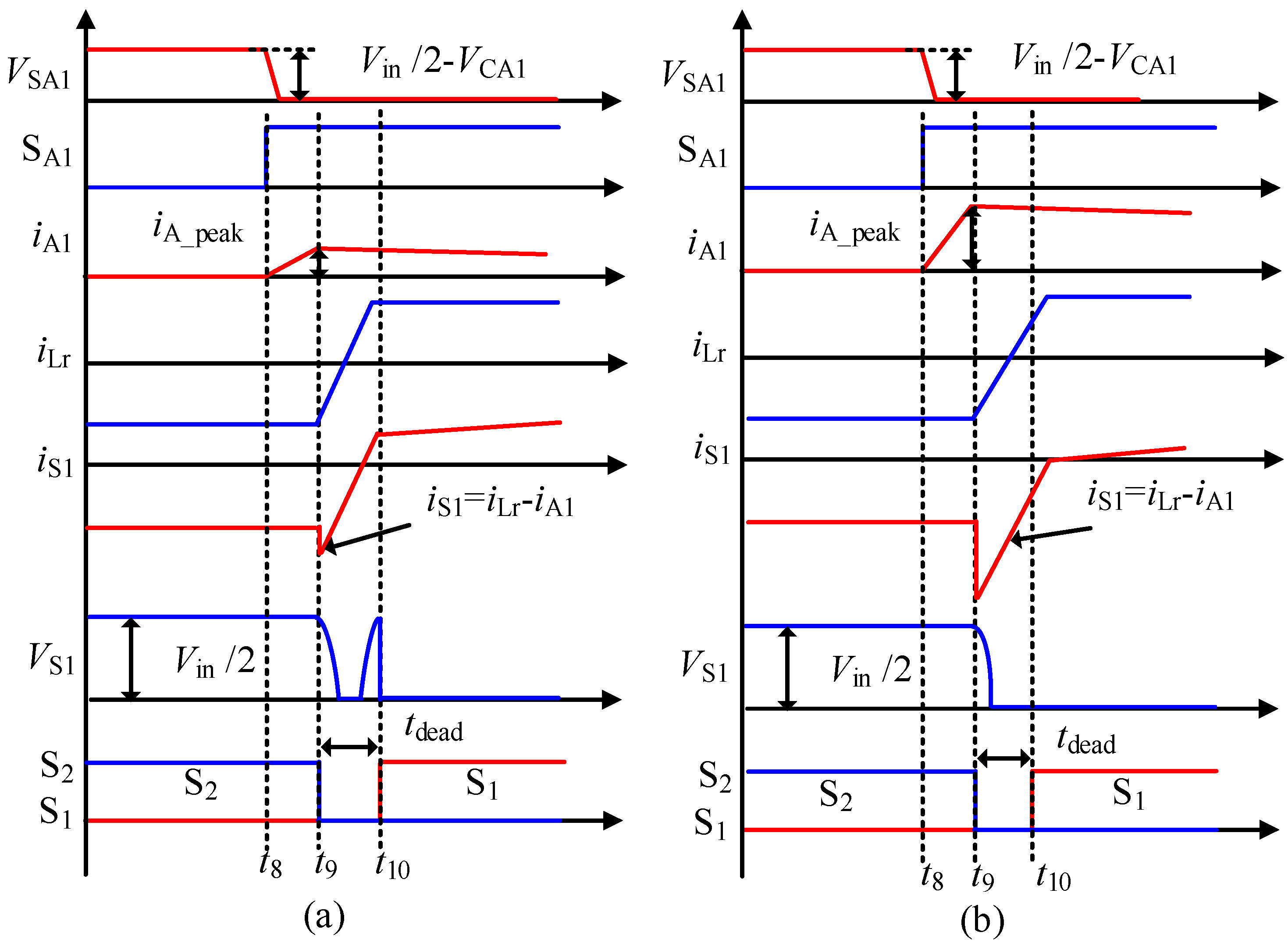
Interval 8 (
Figure 5h,
t7~
t8): At
t7, the main switch S
4 is turned on at zero-voltage condition and the converter reaches a freewheeling stage. The auxiliary current
iA2 increases linearly and will reach zero quickly.
Interval 9 (
Figure 5i,
t8~
t9): At
t8, the auxiliary switch S
A1 is turned on at zero-current condition and the current
iA1 will be built up quickly. At
t9, the main switch S
2 is turned off and the current
iA1 reaches the maximum value
iA_peak.
Interval 10 (
Figure 5j,
t9~
t10): At
t9, the main switch S
2 is turned off and the current
iA1 and
iLr will discharge
C1 and charge
C2 until the voltage of
C1 reaches zero; thus, the zero-voltage turn-on condition for the switch S
1 is realized. At
t10, the main switch S
1 is turned on at zero-voltage condition and a new cycle begins.
With the ACACs, all the main switches achieved zero-voltage turn-on. Considering that the equivalent parallel capacitors
C1~
C4 limit the rising slope of the voltages across the main switches, the main switches are turned off at quasi zero-voltage condition. The auxiliary switches realized zero-current turn-on and zero-voltage turn-off. The auxiliary current is controllable by adjusting the turn-on time of the auxiliary switch S
A. As shown in
Figure 4, the intervals (
t3~
t4) and (
t8~
t9) are used to build the auxiliary current; these intervals can be marked as
tA_build. During the constant-current stage, the charging current is large enough to realize ZVS naturally, the auxiliary switch S
A will not turn-on and the auxiliary circuit does not work. During the constant-voltage stage, the charging current is small, and the auxiliary circuit will work to realize ZVS of the main switches; thus, the full load range ZVS can be realized.
4. Experimental Results
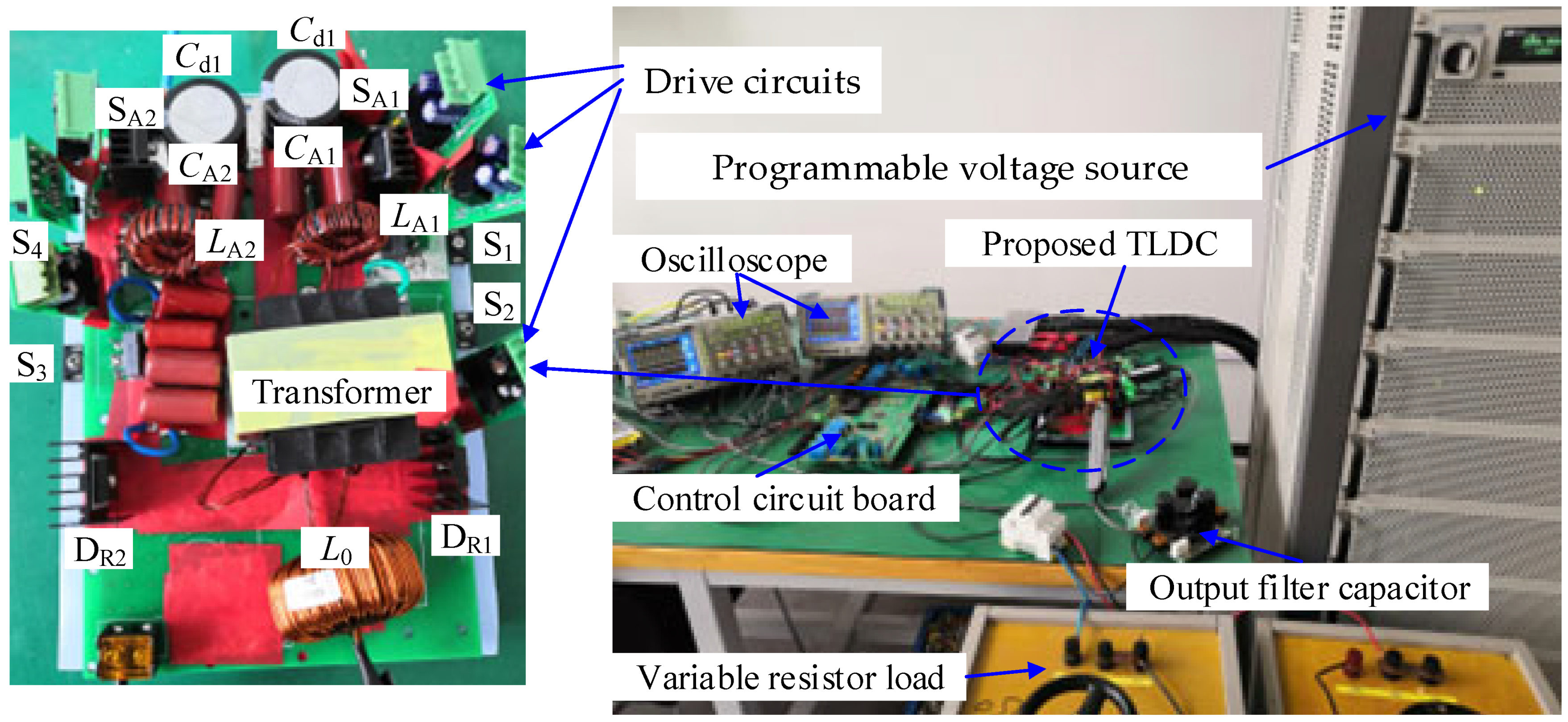
To verify the proposed ZVS ITLDC, a 1.5 kW prototype ITLDC with ACACs is utilized with the specifications shown in
Table 1. When the proposed ITLDC is used to charge EVs, the ACACs mainly play a role in the constant-voltage charging stage. During the constant-voltage charging stage, the charging current changes with charging time and the charging current is relatively small. Then, the ITLDC cannot realize natural ZVS soft switching during the constant-voltage charging stage; thus, the ACACs will work to realize ZVS soft switching. In this experiment, the input voltage is 400 V, which is powered by a programmable DC voltage source. The variable resistor with 80 Ω maximum resistance is used as a load and the output voltage is controlled to 150 V. The snubber capacitors
Cs are added in parallel with the main switches, and the equivalent parallel capacitors
C1~
C4 are increased; thus, the main switches are turned off at quasi-zero-voltage condition. A photograph of the experimental platform is shown in
Figure 8.
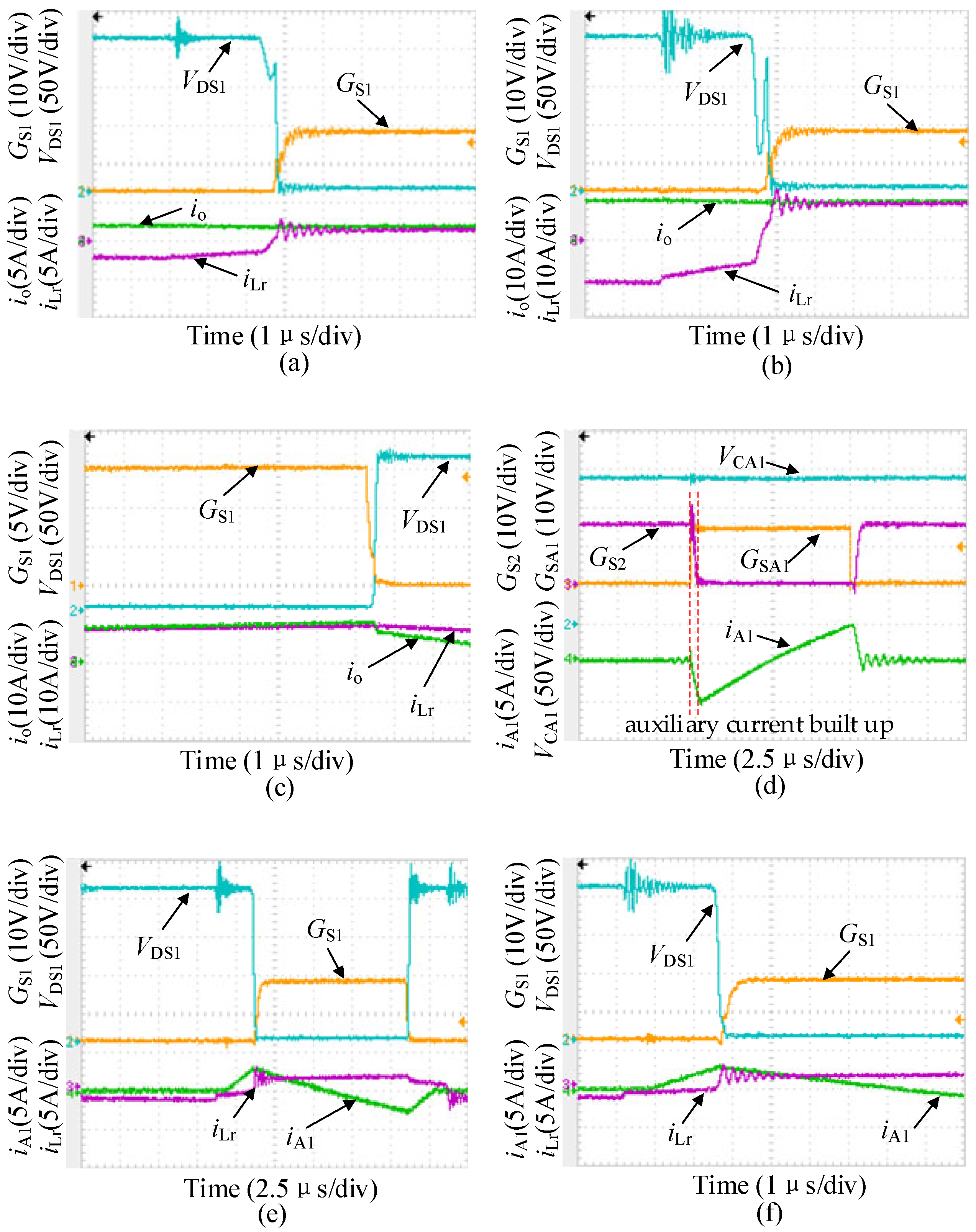
The main waveforms measured are shown in
Figure 9, where
VDS1 is the drain-source voltage of the main switch S
1,
GS1 is the drive of S
1,
io is the output current,
iLr is the current of the primary winding of the transformer,
VCA1 is the voltage of the auxiliary capacitance
CA1,
GS2 is the drive of S
2,
GSA1 is the drive of S
A1, and
iA1 is the auxiliary current flowing through
LA1. The turn-on process of the main switch S
1 without ACACs is shown in
Figure 9a,b. As shown in
Figure 9a, the output current
io is 2 A, and before S
1 is turned on, the voltage
VDS1 is discharged from 200 V to 150 V. As shown in
Figure 9b, the output current
io is 10 A, and before S
1 is turned on, the voltage
VDS1 is discharged from 200 V to 40 V firstly; however,
VDS1 increases to 160 V quickly. In
Figure 9a,b, the zero-voltage turn-on condition of the main switch S
1 is unrealized. However, as shown in
Figure 9c, the main switch S
1 is turned off at quasi-zero-voltage condition. This is because the equivalent parallel capacitors
C1~
C4 limit the rising slope of the voltage across the main switches. In this experiment, 1000 pF snubber capacitors are added in parallel with the main switches and the time-related effective output capacitance of the main switch is 1485 pF (documented in the data sheet); thus, the snubber capacitors
Cs of the main switches are equal to 2485 pF.
In fact, according to (6), to realize natural ZVS, the output current
io should be larger than 38.9 A. When the output current is not large enough to realize natural ZVS, the proposed ACACs can be used to realize ZVS. As shown in
Figure 9d, before S
2 is turned off, the auxiliary switch S
A1 is turned on and the auxiliary current
iA1 increases rapidly from 0 A; thus, the auxiliary switch realizes zero-current turn-on. When S
2 is turned off, the auxiliary current
iA1 reaches the maximum value. The voltage of the auxiliary capacitance
CA1 is steady and the value of
VCA1 is approximately 190 V, which is consistent with the theoretical calculation value. According to (5), to realize zero-voltage turn-on of the main switch, the minimum value of the auxiliary current
iA_peak_min should be 2.8 A. According to
Figure 7, when the output current is 2 A, the auxiliary current should be larger than 2.8 A; in this experiment, the auxiliary current
iA_peak is 3 A. As shown in
Figure 9e,f, with the auxiliary current, the main switch realized zero-voltage turn-on. When the output current is 10 A, the auxiliary current should be larger than 5 A; in this experiment, the auxiliary current
iA_peak is 6 A. As shown in
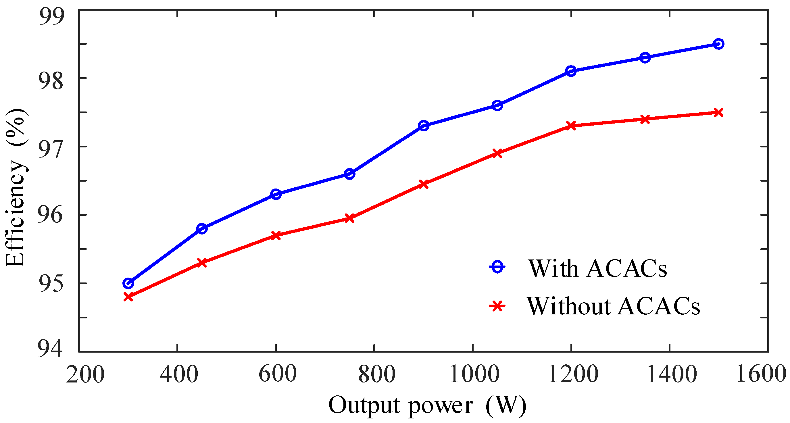
Figure 9g,h, with the auxiliary current, the main switch realized zero-voltage turn-on. With the proposed ACACs, the main switches of the ITLDC realized zero-voltage turn-on. To verify the efficiency, the efficiency of the ITLDC with the proposed ACACs and without ACACs is measured by a HIOKI power analyzer PW6001 and the efficiency changes with the output power are shown in
Figure 10. When the output power is small, the efficiency of the ITLDC with ACACs is slightly higher than that of the ITLDC without ACACs, and when the output power is large, the efficiency of the ITLDC with ACACs is much higher than that of the ITLDC without ACACs.
It is interesting to compare the proposed ZVS method and the state-of-the-art ZVS methods for the four-switch ITLDC. The comparison results are summarized in
Table 2. The auxiliary circuits, soft switching of the switches, soft switching range and current/voltage stress are employed to evaluate the ZVS methods. Each ZVS method has its own advantages. For example, in [
16,
20], wide load range ZVS turn-on and turn-off for all switches is realized; in [
17], wide load range soft switching is realized by the auxiliary circuit with only two switches; in [
19], the ZVS is realized with no auxiliary circuits. However, most of them do not realize the full load range ZVS; thus, with the light load situation—for example, the battery floating charge stage—the converter has to work with hard switching. Many ZVS methods realize wide load range ZVS; however, the ZVS range will decrease when considering the dead time between switches. Although two ACACs are added in the proposed ZVS converter, the full load range ZVS of the main switches is realized. Furthermore, the auxiliary switches realized zero current turn-on and zero-voltage turn-off, and this ZVS method does not increase the current stress of the switches.


