Abstract
This paper proposes the fast and accurate electro-thermal model of the existing Simrod three-phase inverter for an electric vehicle (EV) application. The research focuses on analytical and dynamic electro-thermal models of inverters that can be applied for multi-applications. The optimal design approach of passive filters is presented for the DC and AC sides of the inverter. The analytical model has been established, including a mathematical representation of the inverter and induction motor (IM). The high-fidelity electro-thermal simulation model of an inverter with integrated power loss and thermal model is established. The state-space thermal model (for the IRFS4115PbF device) has been created and incorporated into the MATLAB simulation. The simulation model is then validated with the PLECS software-based thermal model to confirm the accuracy. Indirect field-oriented control (IFOC) is designed for squirrel-cage IM at a maximum power rating of 45 kW and implemented on MATLAB/Simulink. The comparative analysis between the real and simulated results is performed to validate the simulation model at a specific speed, torque, and current. Furthermore, the electro-thermal simulation model has been validated with experimental data using efficiency and temperature comparison. The developed simulation model is beneficial for designing, optimizing, and developing advanced technology-based inverters to achieve higher efficiency at a particular operating range of temperature and power quality. The new European driving cycle (NEDC) speed profile simulation results are demonstrated.
1. Introduction
In the modern era, the technology of battery power EV is gaining utmost importance and is immensely popular. Researchers are investing full effort into manufacturing a reliable and efficient powertrain system [1,2]. Because of growing climate change environmental issues, conventional technology of combustion engine vehicles has transformed into battery electric vehicles (BEVs). BEVs require to be re-energized with grid electricity, and they have no exhaust emissions. The BEVs could be a replacement for combustion engine vehicles because of developments in battery technologies, electric motors, power electronics converters (PECs), and control design strategies [3,4,5,6].
Three different PECs are used in the conventional structure of BEVs, such as AC-DC converter, DC-DC converter, and DC-AC inverter, as shown in Figure 1. The bidirectional DC-DC converter interfaces low voltage (LV) and high voltage (HV) energy storage systems to the DC link. The bidirectional AC-DC converter is used as an on-board charger to transfer energy between battery and grid during charging and discharging operations [1]. The DC-AC bidirectional inverter is used to transfer energy from the DC link to a traction motor, such as a three-phase IM, and back to the battery during regenerative braking. The traction motor is connected to the transmission of the EV to drive the vehicle [4].
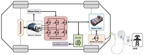
Figure 1.
Four-wheel electric drive vehicles.
As has been previously stated in the literature, the choice of EVs and their control strategy has a significant impact on the development of EV drivetrains. The permanent magnet synchronous motor (PMSM), as well as IM, is suitable for automotive applications. A PMSM is proficient for EVs owing to its unique features such as high torque, high efficiency, high power density, low torque ripple, low noise, and compact size. However, PMSM normally has a constant power limit due to its comparatively limited field weakening capability. Furthermore, the cost is relatively high due to the high cost of permanent magnets. For this reason, an IM could be a suitable solution for EV applications because of its low torque ripple, low cost, wide speed range, and robustness [6].
The inverter is the fundamental part of an EV; it drives the car’s electric motor by controlling the power flow of the battery. The primary concerns for the design of PECs are reduced power losses, high efficiency, less input/output current ripples, reduced size and weight of the passive components, compactness, less total harmonic distortion (THD), high power factor, and high reliability. These factors can be achieved by choosing a suitable semiconductor device. Therefore, semiconductor devices are the main part of PECs. At the moment, WBG semiconductor has superior material properties, as shown in Figure 2, and it is more efficient in high power EV applications in comparison with standard silicon (Si) [4,7,8]. Currently, policymakers and other stakeholders have further increased efforts to strengthen the market share of EVs. To accomplish this objective, power electronics (PEs) researchers pursue to advance the PEs EV system by raising their power density and reducing volume, system cost, and size [8,9].
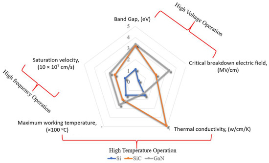
Figure 2.
Material characteristics of Si and WBG (SiC and GaN).
The losses, as well as thermal modeling, are essential for developing converters with performance features such as high efficiency and reliability, high power density, cost-effectiveness, and compact system size [1]. In the literature, various electro-thermal modeling strategies have been reported. The modeling method exploited in software such as LTspice or Saber is highlighted in [10,11]; then again, a major issue concerning this method is huge computational time. The switching energies Eon (i.e., turn on) and Eoff (i.e., turn off) are calculated using the rise and fall time of drain to source current (Ids) and voltage (Vds) of MOSFET. Due to the fast-switching interval, the rise and fall time can be calculated by dividing the entire PWM cycle of PWM into smaller subintervals. The energies are further used to estimate switching loss [12]. In [13], the non-parametric Gaussian process regression (GPR) technique is used to predict missing data points. GPR is used to predict Ids on several Vds and Vgs. The kernel function is applied to extract the information for accurate prediction. The exponential kernel function is used to create a model, but this method is complicated.
The lookup table method has been applied in a simulation to approximate switching as well as on-state losses of the IGBT transistors [14,15]. This method gives an automatic, compact, and accurate model of semiconductors for the PEs inverter’s analysis by the use of the average computational time of the CPUs. Thermal simulation of IGBT modules has been designed to calculate the system’s responses. It is essential to optimize the system, i.e., reducing design cost, increasing reliability, risks or faults occur, time to be powered off when overheating, and calculating maximum switching frequency, which would depend on the junction temperature [16]. The power losses, as well as thermal optimization, have been in general controlled by modifying electrical parameters. The power losses have been estimated by means of electrical loading on the devices and then transformed into a thermal model to generate the junction temperature of the semiconductor devices, as discussed in [17]. The junction temperature is an important parameter for reliability prediction [18]. The passive filters have been reported to be essential to obtain fewer ripples and high-efficiency responses from the converter, and system cost, weight, and size are greatly impacted. Hence the optimum design is mandatory with a variation of the switching frequency [19]. Analytical-based model is an effective method for controllability analysis, stability analysis, and control system design [20,21,22].
This research aims to design an accurate and fast electro-thermal high-fidelity simulation model for the inverter, which would precisely reflect the functional behavior of the Si MOSFET-based existing inverter. Therefore, the manufacturer-based data are applied through the interpolation method, depending on the voltage, current, and junction temperature. This model calculates the instantaneous power loss at every switching interval, regardless of how fast your switching frequency is. The transfer function of the thermal model of MOSFET is designed as a virtual sensor to convert power loss into junction temperature. These features make the model unique from literature. The heatsink model is created to calculate the inverter case temperature. The complete electro-thermal model runs such as a real inverter, and the efficiency depends on temperature, voltage, and current. The WBG devices can easily be integrated into the inverter model to operate at higher switching frequencies and analyze the power loss and temperatures of the inverter at a higher frequency for the case of GaN and SiC. Moreover, the model allows the pre-establishment and the post-analysis of the system by varying control design, circuit parameters and operating switching frequency, etc.
This paper has been arranged into seven sections. Section 2 comprises the passive filter design to minimize the ripples at the AC and DC sides of a multi-purpose inverter. Section 3 illustrates the inverter modeling and control, inverter and motor design parameters, analytical model of the inverter and IM, and control strategy for IM. Moreover, space vector (SV) pulse width modulation (PWM)-based IFOC control is designed using steady-state feedback analysis and implementation on the simulation model. In Section 4, an electro-thermal model of an inverter is created. The high-fidelity MATLAB/Simulink simulation is developed for the three-phase inverters, and the power losses are calculated through a datasheet-based lookup table technique. The designed state-space thermal model has been incorporated as a virtual sensor to convert power losses to the temperature. Furthermore, the prediction of the converter’s efficiency by means of total power loss has also been demonstrated in the section. Section 5 illustrates the validation of the simulation model with experimental high-frequency data of an existing inverter. Finally, Section 6 presents the electro-thermal simulation results, and Section 7 is the conclusion.
2. Passive Filter Design
This section demonstrates the design approach of passive filters to minimize ripples at the DC and the AC sides of the inverter [1,19]. The passive filter is designed according to the power rating of the converter by considering resistive load [2].
2.1. AC Filter
The inductor-capacitor-inductor (LCL) filter is designed as an AC filtering to filter out the ripples and improve power quality for the bidirectional multi-purpose inverter. The two inductors and one capacitor are used as filters per phase: is inverter side inductor, is a parallel capacitor, and is the load side inductor calculated as in Equations (1) and (2), referred to in Figure 3.
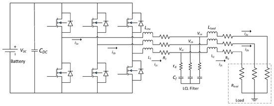
Figure 3.
Passive filters of the inverter.
In Equation (1), the value of n would be 4 [23] for a three-phase inverter, (A) is the rated current at the load side, (W) is load power, (Hz) is operating switching frequency, is 40%, and (V) is phase-to-neutral voltage. AC capacitor filter at three phases could be calculated as Equation (3).
where (Hz) is AC frequency and (W) is rated load power.
Attenuation factor which would indicate an allowable ripple in the inductor, and a switching inductor is represented in Equation (4). has to be minimized while maintaining a stable and cost-effective filter [24].
is considered 5% for this design. The factor r is derived by rearranging the above equation and represented in Equation (5).
The other load side inductor is determined by multiplying with as expressed in Equation (6).
After filter design, it is essential to calculate the resonance frequency (Hz) as shown in Equation (7), which must meet the required criteria as well as validate the LCL filter design. The stable region of is between 10 times the rated AC frequency (i.e., 50 Hz frequency in the case of grid applications, or maximum rated speed of the motor can be considered for electric motor applications) and half of switching frequency. These criteria avoid issues in the upper and the lower harmonic spectrums.
The remaining variable describes passive damping that could be added in order to avoid oscillations. The damping resistor can be calculated by the use of capacitor and resonance frequency value as represented in Equation (8).
2.2. DC Filter
The DC link capacitance is used on the battery side of the inverter. The DC filter helps to reduce the ripples on DC voltage. It is quantified using these Equations (9) and (10) [19,24].
is DC link voltage, is average power that is flowing into a converter, (V) is the amplitude of the permittable DC link voltage ripple, set at 3%, and resistance can be calculated from average power and DC link voltage.
3. Inverter Modeling and Control
This section describes the analytical modeling of inverter and IM. The closed-loop IM control of a three-phase inverter is developed for EVs. This controller considers outer loop speed control, inner loop flux control, and current control, which has been shown in a block diagram in Figure 5. The controller drives six switches of a two-level DC-AC inverter for tracking the motor’s reference speed, torque, and currents. Such a control strategy is incorporated with a complete dynamic electro-thermal simulation model in MATLAB to analyze losses and temperature performance. After developing the simulation model, the results are compared with real inverter data. The IFOC control design approach and implementation for IM are explained in detail [4,5,6].
3.1. Parameters and Devices
The details about the parameters and devices of the inverter and IM are stated here. These quantities are exploited in the simulation model design. The three-phase inverters and IM are listed: DC voltage, switching frequency, ambient temperature, Si MOSFET devices, passive filters, frequency, and power rating.
3.1.1. Inverter Parameters
The battery voltage and switching frequency are the same as the existing inverter. The AC and DC passive filter values have been calculated from the abovementioned equations. This paper presents the modeling of the inverter, which is commercially available. Therefore, only DC link capacitors are used in simulation as DC filters. The conduction and switching characteristics of Si MOSFET are applied from the manufacturer datasheet to design an electro-thermal model of an inverter and for model validation using experimental data. The specifications of the inverter are given in Table 1. The inverter and motor of Simrod EV are used to design the model. The details about Simrod EV are mentioned in [25]. According to the Simrod three-phase inverter topology, 16 upper and lower MOSFETs are connected in a parallel configuration, as demonstrated in Figure 4. The current is distributed in all MOSFETS. The same topology of an inverter is proposed in the simulation.

Table 1.
Inverter parameters.
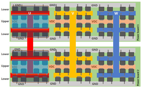
Figure 4.
Three-phase Simrod inverter board.
3.1.2. Induction Motor Parameters
Parameters of squirrel-cage IM have been expressed in Table 2. These quantities are used to model the electric motor and IFOC design.
Table 2.
Induction motor parameters.
3.2. Analytical Modeling of Inverter
An analytical or mathematical model is useful for understanding the dynamics of a system. The model is developed with the details of the inverter and its filter parameters. Analytical modeling is inspiring to perform due to its complexity.
This model can be alterable according to the need and classification of the inverter. It can also be used for an inverter’s stability analysis to check the system’s stability and the closed-loop control design [26]. An analytical-based model is constructed for the inverter, as depicted in Figure 3. The first-order differential Equations (11)–(22) have been derived and validated with the MATLAB/Simscape model in an abc frame of reference for the three-phase inverter is presented in Figure 3 [1,23]. This converter model can be applicable for multi-purpose applications such as grid-connected inverters, bidirectional EV chargers, etc.
The input voltages and currents are calculated using the above expressions.
(V) are three-phase input converter voltages, (A) are AC currents and are duty cycles, (Ω) is the load resistance, (V) are the voltages across the filter capacitors, and (V) is DC voltage.
3.3. Analytical Model of Induction Motor
The Ims are commonly accepted as a more suitable option for electric vehicle application because of their rigidity, reliability, lower cost, and less maintenance. Nevertheless, Ims’ speed as well as torque controls are quite complicated because of their non-linear and complex structure. Based on IM’s dynamic model, various control strategies have been developed to surpass control challenges. Hence, the dynamic model of an IM is important for the design of a control approach to achieve high efficiency. Therefore, the dq model of IM is considered in the simulation design to implement closed-loop IFOC for the motor drive. The analytical model of IM has been described in synchronous reference frame [5,6] by means of the Equations (23)–(29) [27] as follows.
where (Ω) is the basic resistance and the dq variables () (V) and () (A) are stator voltages and the stator currents, respectively. Moreover, dq variables () (V) and () (A) are rotor voltages and the rotor currents, respectively. (rad/s) is the angular speed of IM, is synchronous speed, is slip speed, and represents the pole numbers. (Ω), (Ω), (H), and (H) are stator and the rotor resistances, stator leakage, rotor leakage, and mutual inductances, respectively. is the rotor self-inductance (. Lastly, (Nm), (Nm), (Nms), and ) are electrical and load torques, coefficient of friction, and the moment of inertia, respectively.
3.4. Control Strategy
The IFOC is the utmost popular control approach in the reported literature. This approach is used to accomplish speed control of IM. IFOC can provide decoupling between the current references linked to the torque and flux in the machine. This reflects that the stator current of an IM is decoupled into torque and flux-creating components. The flux and torque components can be controlled individualistically and sustained in a synchronous frame of reference. The current of the direct axis acts to control the flux component, while the current of the quadrate axis controls the torque component. Figure 5 is illustrated for speed, flux, and current control strategy of IM using Space Vector Pulse Width Modulation (SVPWM) [4,5].
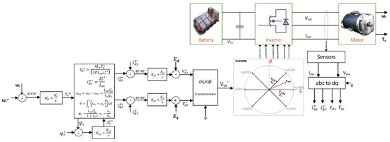
Figure 5.
SVPWM-based indirect field-oriented control design (IFOC).
The SVPWM is a progressive computation technique that can generate PWM signals to drive the MOSFET gates. This paper develops the simulation model according to an existing inverter’s specification. Therefore, the SVPWM technique is applied to generate 10 kHz PWM signals. Figure 5 shows the SVPWM-based IFOC. This SVPWM technique delivers a fixed switching frequency. This SVPWM method is used to approximate reference voltage instantly by combining switching states according to space vectors. As shown in Figure 5, the reference voltage is approximated using the switching vectors and null vectors. Moreover, is sampled with the fixed switching frequency , and the next subsequent sampled value is used to evaluate stationary times , , and using Equations (30)–(32), where signifies modulation index and is DC link voltage [4,5,6,28].
where dq reference variables stator voltages and the stator currents are () and (), respectively. is a reference and is a space vector rotor flux, is the reference and is the space vector stator flux, is synchronous speed, is slip speed, is flux angle, (s) is stator time constant, (s) is rotor time constant, and represents pole numbers. , and are proportional gains, and , and are integral gains of proportional integral (PI) controllers for speed, flux, and current, respectively.
The following Equations (33)–(39) are used for control design and implementation. In Figure 5 of the IFOC control approach, mathematical equations are mentioned in the block, which are used for the control implementation. It can be observed through equations. Torque and flux requirements can be easily translated into current requirements.
Flux angle is calculated using this expression, and it is used for the transformation of the reference frame to the dq frame.
Reference flux can be calculated as Equation (37). It is used for field weakening. The flux controller is used for improving the flux dynamics in the case of varying reference flux, where and are rated speed and rated flux, respectively.
The flux controller generates reference and current reference can be calculated using Equation (38).
Reference torque coming from speed controller producing current reference , and it is calculated as Equation (39),
The control references such as and in d-q frames come from current controllers, which have also been compensated by the back electromotive force. The reference dq voltages with the back electromotive force compensation ( and ) is calculated as Equations (40) and (41). These are used to generate SVPWM signals to drive the inverter [27].
3.5. Control System Design
Three feedback control of speed, flux, and current are designed using the transfer functions of plants. The design methods of the controllers are illustrated below.
3.5.1. Speed Control
The demand torque of IM comes from the speed controller. The PI controller is designed to track the reference speed for the IM. The proportional gain and integral gain are tuned to achieve the desired overshoot, rise time, settling time, and crossover frequency (ωcp). The speed controller is designed using a plant model and sensor delay with load torque as shown in Figure 6, where , , and are electrical torque, load torque, coefficient of friction, and the moment of inertia, respectively [4,5,29].
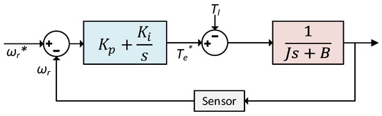
Figure 6.
Feedback speed control loop.
3.5.2. Flux Control
The second PI controller is designed for flux control. The flux controller is designed using the plant transfer function, as shown in Figure 7, where is the rotor time constant.
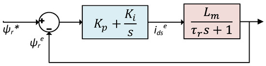
Figure 7.
Feedback flux control loop.
3.5.3. Current Control
The IFOC has been designed based on space vector PWM control, with the fixed 10 kHz switching frequency for a manufacturer-based existing inverter. In this control scheme, measured and components have been compared to references (by reference flux) and (by reference torque) as presented in Figure 8. The two PI current controllers are working together and provide voltage references and , which are used for the generation of PWM signals. As in Figure 8, computational time delay models a time delay between ADC sampling instant as well as a consequent PWM duty cycle. Such time delay is the half of the PWM period, where the sampling period and the PWM period are the same, so a computation time delay . The current controller is designed using computation time delay, plant model, and sensor delay, as shown in Figure 8, where is the current model time constant and is the combined motor resistance [29].
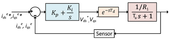
Figure 8.
Feedback current control loop.
A closed-loop plant transfer function was used to perform a disturbance rejection analysis. The presence of input and output disturbances provided information about the designed controller. When a disturbance enters the system, the disturbance rejection plot could reveal information about the controller’s effectiveness. The system responded quickly to controller disturbances in order to return to a stable state. The closed-loop step response of input and output disturbance rejection of speed control, current control, and flux control is shown in Figure 9. The formulation of each controller and their tuning is carried out by the use of the gain margin (gM) with gain crossover frequency (ωcg) as well as the phase margin (PM) with phase crossover frequency (ωcp). The PI controller’s proportional gain and integral gain are set to achieve desirable controller performance (i.e., rise time, settling time, overshoot). The speed, flux, and current feedback controllers are depicted in Table 3.
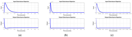
Figure 9.
Closed–loop disturbance rejection response of (a) speed controller, (b) flux controller, and (c) current controller.
Table 3.
IFOC control of IM.
4. Electro-Thermal Modeling
The power loss of the half-bridge PEs module has been derived mathematically. The inverter’s total power losses, on the basis of conduction and switching losses, are presented in Figure 10.
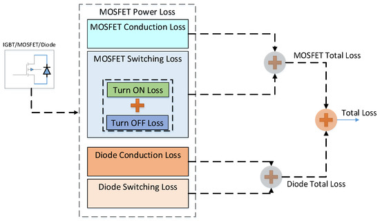
Figure 10.
Total power losses block diagram of MOSFET.
The DC supply is connected as an input to the three-phase inverter, and three phases of an inverter as output are connected to the three-phase electric motor. During the operation, each leg of the inverter generates heat. The three-phase electro-thermal simulation model of the entire inverter has been established by concatenating three half-bridge PE modules along with their thermal model and power loss. The current and voltage of each leg pass to the power loss model to estimate the power loss of the inverter half-bridge. The thermal model takes the power loss as input and estimates the junction temperature of MOSFET and diode. The heat flow of MOSFET from the thermal model will enter the heatsink model and provide the heat sink temperature. The superposition of all losses computes the total power average loss for all three half-bridge PE modules. Inverter’s block diagram representation with a model of power loss and coupled thermal and heatsink model has been demonstrated in Figure 11.
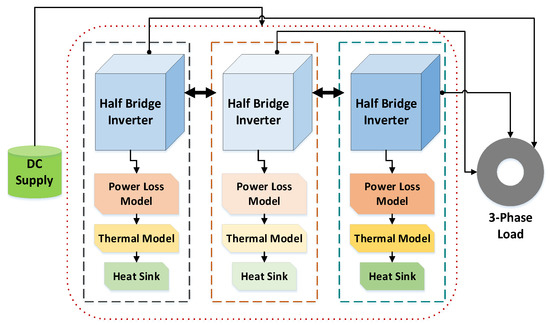
Figure 11.
Inverter’s electro-thermal model block diagram.
4.1. High-Fidelity Power Loss Model
In the following section, the power electronics three-phase inverter model has been designed in the MATLAB Simulink, transforming the DC power to AC power at a fixed 10 kHz switching frequency. Loss assessment and thermal analysis of electronic systems is a major concern because of their impact on system life, reliability, and efficiency. Power loss because of the PWM switching period of a power electronic device has been divided into switching loss (turn-on and the turn-off loss), conduction loss, and the total power loss (with the addition of the switching and the conduction loss) [14,18]. Piece by piece modeling of the single module first, after that accumulation of the three modules, afterward assembling to develop the electro-thermal model of the three-phase inverter, as explained.
4.1.1. Conduction Power Loss
In this method, conduction power loss is anticipated using datasheet characteristics by Equation (42).
(V) and (A) represent forward saturation voltage and the drain current of MOSFET. and are functions of a junction temperature (°C) and depend on one another.
The voltage could be calculated by interpolation using lookup tables. The lookup table reveals datasheet specified characteristics. Therefore, during each sampling step of a simulation, it can deliver information consistent with the datasheet specs of a power module. For example, Figure 12 shows the input and the output relation of a lookup table for the conduction loss [18,30,31,32,33,34].
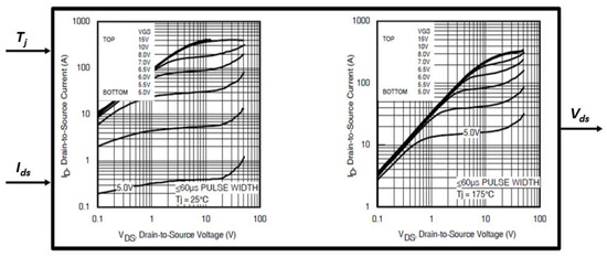
Figure 12.
Lookup table to determine of MOSFET.
Integrating instantaneous power loss over the switching cycle would provide the average value of MOSFET conduction losses [30,32], as shown in Equation (44).
In such a way, MOSFET conduction loss could be calculated by multiplying at every simulation time step a sample data of with .
Estimating conduction loss through a body diode is comparable to the above Equation (42) for MOSFET. The diode conduction loss could be found by Equation (45).
(V) and (A) represent a forward saturation voltage and the diode’s current. and are functions of a junction temperature and dependent on one another.
The average diode conduction losses across the switching period (s) [30,32], are expressed in Equation (47).
4.1.2. Switching Power Loss
Precise estimation of the switching loss in a device is essential. The switching loss offers information about the amount of lost energy because of on-state to turn-off and off-state to turn-on transitions [18,30,31,32,33,34]. Application of a complex strategy is needed for quantifying the on and off losses with the small simulation step size. Owing to switching, the lookup table [11] method was preferred to estimate switching power loss due to the complex physics process of switching. With the aid of the switching energy values, i.e., Esw on (mJ) and Esw off (mJ), one could estimate switching power loss in a device. Calculation of switching energy by the use of datasheet specifications has been performed as the function of drain current and the junction temperature [14,18,34].
where k denotes the kth PWM switching pulse. Switching characteristics from the datasheet for switching the energy losses (Esw on and Esw off) of MOSFET against the drain current versus the junction temperature have been represented in Figure 13. At each kth time step of a simulation, the total energy is calculated by Equation (50).
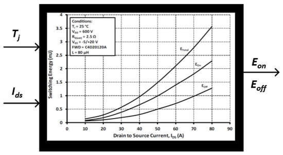
Figure 13.
Lookup table to determine energy loss of MOSFET.
Given a switching frequency (Hz), switching power loss is estimated as represented in Equation (51).
Now, switching loss for a body diode is calculated by reverse recovery characteristics [19]. In that case, reverse recovery loss is a function of the diode current as well as its junction temperature in Equation (52). The Err is estimated using the datasheet characteristic according to Figure 14.
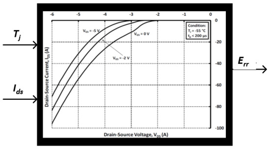
Figure 14.
Lookup table to determine diode Err.
(A) is the forward current of a diode, as depicted in Figure 14. Therefore, the switching power loss calculation across a diode is performed as in Equation (53).
The switch’s total average power loss and body diode are computed with Equation (54).
4.2. Thermal Modeling and Implementation
MOSFETs are susceptible to the working temperature; in addition, thermal cycling is the major reason for various PE component failures and reduction in lifetime. MOSFET’s temperature impacts the design of a power electronic converter; also, the cooling system has an influence on the size of a converter. The maximum operational temperature of a MOSFET indicates the cooling capacity of the device required and what kind of cooling is required, for example, liquid cooling or air cooling with a proper heatsink [35].
In the operation of the semiconductor devices, for instance, in the course of turn-on and -off, conduction and the switching losses depend on the device’s temperature (and vice versa). Therefore, careful design is essential for confirming accurate functionality with all the temperature-dependent conditions over the entire expected temperature range.
The power losses have been injected into the fourth-order, Cauer-type, thermal network, as represented in Figure 15, and the thermal parameters have been extracted from the producer’s MOSFET datasheet. Equivalent thermal impedance Zth of MOSFET and body diode are calculated using Equation (55) and the time constant (56).
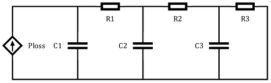
Figure 15.
Third-order Cauer-type thermal network.
Now, MOSFET and the diode junction temperature could be calculated by using our designed state-space thermal model. Such a model has been based on the one element section of the Cauer network, which would total a third-order equivalent thermal resistance and equivalent thermal capacitance network for MOSFET or the diode, about which the details have been given in the datasheet. Such a compact thermal model consists of two inputs: the total power loss ( (W)) and case temperature (Tc (°C)) of an inverter, and its two outputs are heat flow (Pc (W)) and junction temperature (Tj (°C)) (Figure 16). The basic heatsink has been modeled in the MATLAB/Simulink according to thermal conductivity from a case to the sink and from a sink to the ambient (convective for air cooling). It is at that time incorporated with the thermal model that determines heat flow and an ambient temperature, the case, and sink temperatures, as presented in Figure 16. The state-space thermal model has been defined by (57) and (58).
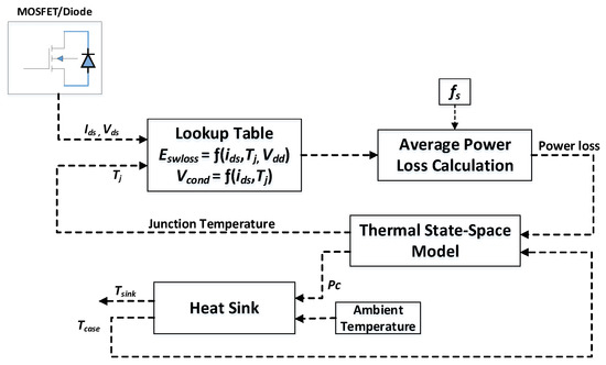
Figure 16.
Power losses and thermal model block diagram.
The procedure mentioned above is a simple method for estimating the power module’s junction temperatures; in addition to this, the transfer function of the thermal model is easily executed in the simulation. The state-space thermal model is implemented after discretization in the MATLAB simulation (with the integration of the non-linear loss model). In the lookup table block of Figure 16, the switching and conduction characteristics of MOSFET are modeled using Ids, Vds, and Tj. Average total power loss is calculated by accumulating average switching and conduction power loss. The thermal state-space model is further applied to estimate the junction temperature and total heat flow. The heat flow is used as the input of the heatsink model to estimate the sink temperature and case temperature with respect to the ambient temperature.
4.3. Efficiency Estimation
Inverter efficiency is essential for observing the total performance of a system. The efficiency of an inverter is estimated using power loss. The efficiency has been calculated as the percentage with the aid of relation between total average power loss and the output AC power of an inverter according to Equations (59) and (60).
5. Experimental Validation
This dynamic simulation is applicable for overall system parameters such as current, voltage, speed, torque, efficiency estimation through output power, and total average power loss of a three-phase inverter with closed-loop motor control.
The IM model, IFOC controller, complete loss model, and thermal model with three-phase inverter are integrated into MATLAB Simulink. This simulation can examine the controller performance, with power losses, thermal characteristics, and system efficiency.
5.1. Installed Setup and Measurements
The 96 V and 200 Ah LiFePO4 battery pack feed a Simrod inverter. The squirrel-cage IM with the four poles 15/45 kW (rated/max.) drives the rear axle through a reduction with a factor of 7.13. The outer diameter of the wheel was 576 mm [36].
NEDC or other speed profiles can be applied as a reference speed. In this way, the designed controllers’ performance can be investigated. Generally, the speed profile such as NEDC and WLTC are in km/h or m/s. However, the controller takes input reference speed in RPM. Therefore, it is essential to convert from m/s to the RPM using the relation represented in Equation (61). As an example of the NEDC speed profile, the speed of the motor (in RPM) has been attained as an average of both motorized wheel speeds, which is multiplied by a gearbox ratio of 7.13. The NEDC speed profile in RPM is shown in Figure 17.
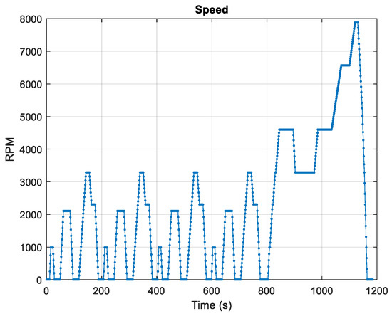
Figure 17.
NEDC speed profile in RPM.
As mentioned in Section 3.5.1 of speed control design, the rotational speed (RPM) can be calculated using the s-domain transfer function as represented in Equation (62). The relation is modeled in simulation to estimate the speed using load and electrical torque.
The thrust can be calculated using the relation of torque, thrust, and radius of the wheel, i.e., m]. Using the above Equations (61) and (62), the dependency of speed (m/s) on thrust can be calculated as Equation (63).
where (Nm), (Nm), and are electrical torque, load torque, coefficient of friction, and the moment of inertia, respectively. (N), (N), (m), and are the electrical thrust, load, radius of the wheel, and gearbox ratio, respectively.
The source (battery), inverter, and motor are connected in the arrangement [36], as shown in Figure 18.
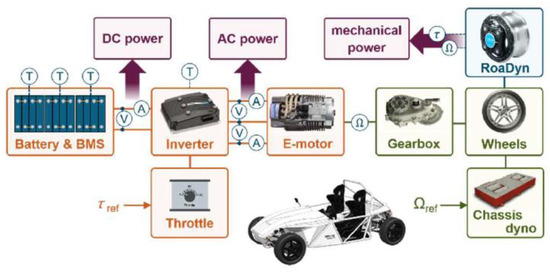
Figure 18.
Instrumental powertrain schematic view.
The data are logged from the installed test setup [36], as shown in Figure 19, and used to validate the simulation model. The DC side of the three-phase inverter is connected to the battery, and the AC side is connected to the three-phase induction motor. DC and AC voltages and currents are measured using transducers. The Kistler RoaDyn wheel force transducer measures the 6-DOF forces and the wheel’s speed and torque. The throttle device is connected to the inverter to adjust the throttle input. The electrical current and voltage are measured on the inverter’s DC as well as AC sides using the three voltage probes (Tektronix P5200A) and the three zero-flux current transducers (LEM IN 1000-S) [36].
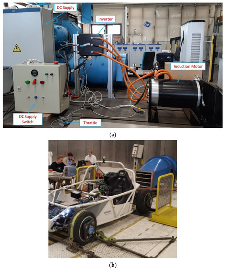
Figure 19.
Installed setup; inside current sensors (a) and Simrod EV on chassis dynamometer (b).
The data acquisition has been made with the Siemens (SCADAS) mobile system at a different sample rate that depends on the bandwidth of examined quantities. Particularly for phase voltages, high-frequency measurement was needed. The square wave character of the PWM AC voltage refers to the presence of an inverter’s 10 kHz switching frequency. Therefore, the electrical quantities such as voltages and currents are logged at a sample rate of 204.8 kHz. In addition to the 92 kHz cut-off frequency built-in anti-aliasing filter, an additional low pass filter (zero phase) of 5 kHz cut-off frequency has been fitted. These filters wash out switching harmonics from high-frequency Yokogawa measurements.
5.2. Simulation vs. Real Results
Simulation results are generated by setting the parameters of the inverter and IM as mentioned in Table 1 and Table 2. In this section, a comparison takes place between the simulation results and the existing inverter data of the Simrod EV. Real high-frequency data are logged by considering three different cases for this comparison. In case-1, the reference speed was set at 2760 RPM, and the motor tracked the command with measured torque of 105 Nm. In case 2, the reference speed was set at 5382 RPM, and the torque became 24.6 Nm, and in case 3, the reference speed was set at 7700 RPM, and the torque was 14.5 Nm. Thus, the simulation results of the three-phase currents are perfectly matched with existing inverter data. Comparison plots are shown in Figure 20, Figure 21 and Figure 22. Hence, the inverter’s dynamic simulation model with control is as accurate as the inverter.
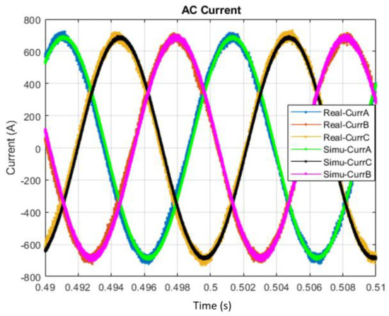
Figure 20.
Case 1: speed = 2760 RPM and torque = 105 Nm.
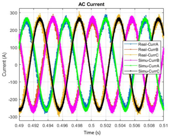
Figure 21.
Case 2: speed = 5382 RPM and torque = 24.6 Nm.
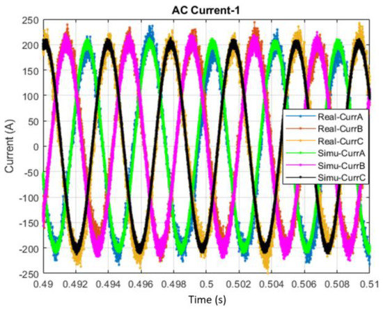
Figure 22.
Case 3: speed = 7700 RPM and torque = 14 Nm.
5.3. Thermal Model
After implementing the thermal model of the MOSFET and body diode in MATLAB, it was validated with a thermal model (based on Si IRFS4115PbF device) of PLECS software. Due to the lack of experimental thermal data, the temperature rise of the electro-model has not been validated by comparing it with experimental results, as stated similarly in the paper [37]. However, in PLECS software, the electro-thermal model is created with the library of the manufacturer’s device, which has conduction, switching, and thermal characteristics. It has been observed that the response of the junction temperature and heat flow coming from developed MATLAB simulation is similar. PLECS versus MATLAB comparison results have been presented in Figure 23.
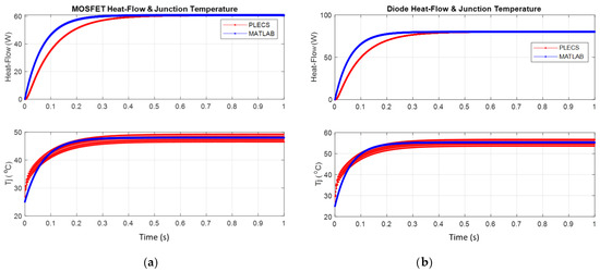
Figure 23.
Thermal model PLECS validation of (a) MOSFET, (b) diode.
5.4. Efficiency and Temperature
In this section, the efficiency and case temperature of the simulation model is validated with actual experimental results at specific speed and torque. The thermocouple is mounted on the case of the inverter to monitor the case temperature. The ambient temperature during the test was 25 °C. It depends on case temperature; therefore, it is considered the same as the experimental data in the simulation model. Designed passive filters in Section 2 can be applied to reduce the ripples. However, in the Simrod inverter, there are no AC filters, and the inverter is directly connected to the IM. The loss of DC link capacitors is negligible because 44 capacitors are connected in parallel. Therefore, it has not been included in the electro-thermal modeling of an inverter. Three cases are considered for validation, as depicted in Table 4. Therefore, the simulation model gives more or less similar results to the real Simrod EV inverter.
Table 4.
Actual vs. simulation validation.
6. Simulation Results
This research objective is to design a closed-loop electro-thermal model of an EV inverter and validate it through real data. Therefore, the complete MATLAB simulation of an inverter with IM control has been developed. According to Figure 24, results are obtained from the simulation model using the NEDC speed profile in Figure 17. In the simulation, nearly three cases are produced by varying the load torque of a motor. The load torque is changed from 10 Nm to 105 Nm from 268 s to 278 s at an NEDC speed of 2106 RPM, as shown in the zoom plots of Figure 24. Similarly, the other two cases produced the torque of 24.6 Nm (from 850 s to 890 s) and 14 Nm (from 1075 s to 1095 s) at NEDC speeds of 4600 RPM and 6571 RPM, respectively, as shown in zoom plots of Figure 24. The ambient temperature is considered at 25 °C. The implemented controllers track the speed and torque reference command generated by the speed controller, as depicted in Figure 24. The efficiency (%), case temperature (°C), and power flow (kW) of three cases of the inverter are investigated using a simulation model, as shown in Figure 25. The zoom plots of Figure 25 depict the efficiency and case temperature are similar as declared in the experimental results of Table 4. The simulation results of Figure 25 reflect the efficiency and temperature of case-1, case-2, and case-3 at time intervals of 268–278 s, 850–890 s, and 1075–1095 s, respectively. The simulated efficiencies and temperatures for case 1 are 96.5% and 87 °C, for case 2 are 97.5% and 51.5 °C, and for case 3 are 97.8% and 45.2 °C. The simulation model estimates the junction temperature of MOSFET and diode by using a thermal model as presented in Figure 16. These junction temperatures are used for power loss calculation for the next iteration. The power loss (W) in power electronic modules of the inverter and junction temperature (°C) of the MOSFET and the diode of each leg for the entire NEDC speed have been depicted in Figure 26. Three-phase inverter currents (A), voltage (V), conduction power loss (W), and instantaneous switching power loss (W) of an upper and a lower MOSFET as well as body diodes are depicted in Figure 27 and Figure 28. Thus, this accurate simulation model of Si-based MOSFET can be applied to design and optimize the new WBG technology-based EV inverter. The simulation model can be parameterized easily by varying the devices, i.e., GaN, SiC, and Si materials, switching frequency, input/output voltage, power rating, motor parameters, control gains, and operating range of temperature. The analysis can be performed to enhance inverter efficiency, power quality, and control system performance. Due to the limitation of Si-based MOSFET devices, it is not possible to increase the switching frequency beyond 20 kHz. However, there is no limit to this simulation model for investigating performance and power quality by parameterizing according to the WBG-based power electronic devices. WBG can operate at high switching frequencies. Using the simulation model, it can be possible to analyze the inverter’s efficiency at higher switching frequencies and examine temperatures to meet the device’s operating temperature range. A developed simulation model can also be useful for predicting the system’s reliability by preparing an appropriate algorithm.
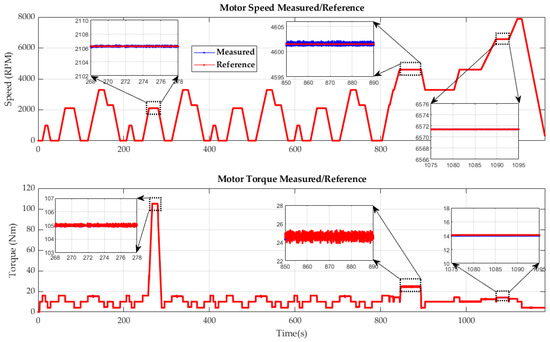
Figure 24.
Speed and torque control reference vs. measured.
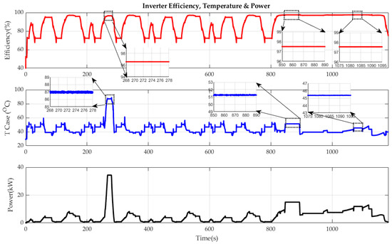
Figure 25.
Inverter efficiency, case temperature, and power.
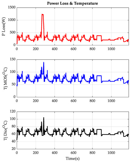
Figure 26.
Power loss and junction temperature.
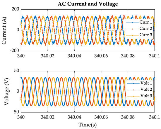
Figure 27.
Three-phase inverter current and voltage.
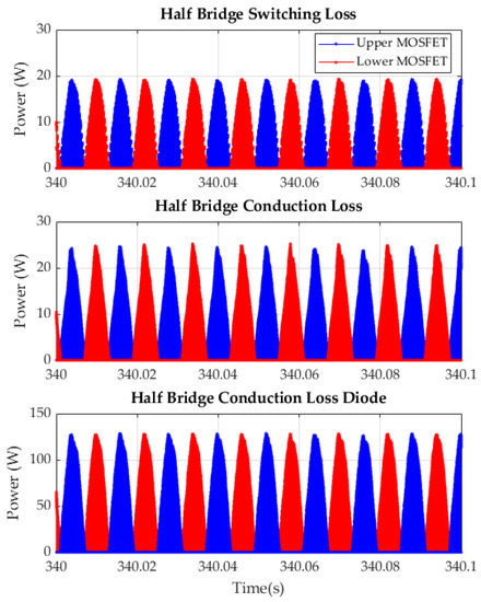
Figure 28.
Instantaneous power loss of MOSFET and body diode.
7. Conclusions
This research proposes a rapid and accurate simulation method for a power loss as well as the thermal estimation of the three-phase inverter, which is based on the manufacturer’s datasheet characteristics. The work was performed to derive linear and non-linear modeling of the multi-purpose inverter and IM for EV’s application. Dynamic simulation of three-phase inverter had been performed to estimate efficiency and power loss, including conduction and switching loss in the MATLAB Simulink innovatively by lookup table technique. Electro-thermal model of an inverter has been developed to estimate the device’s junction and case temperatures. The model is validated using experimental data for three industrial mission profiles (speed and torque). The developed model shows a close similarity with the experimental values of efficiency and case temperature. This scalable parameterization-based high-fidelity dynamic simulation tool can be beneficial for the design and development of power electronic systems. This tool could be used to enhance system efficiency and power quality by modifying device parameters using advanced technology, namely GaN, SiC, and Si materials, and the switching frequency over a certain operating range of temperature. The designed simulation model makes it likely to develop EV inverters to achieve high power density, reduced size, weight, and volume. The developed electro-thermal model can be easily applied to design and develop traction inverters and charging systems for EV applications. This electro-thermal model can be integrated with the MOSFET of power electronic converter, only need to parameterize according to the specification and device properties. The developed closed-loop simulation model can also be used for control design optimization to make it robust.
The accurate electro-thermal model of the power electronic converter plays an important role in the design and development of modern PE converters. Nevertheless, new applications require a highly efficient converter design with low weight and volume, with WBG devices being implemented to operate at high switching frequencies. Future research will focus on this area.
Author Contributions
Conceptualization, H.R.; formal analysis, H.R.; investigation, H.R., M.E.B., A.M.R., A.Z., T.D., M.S. and O.H.; writing—original draft preparation, H.R., A.M.R. and A.Z.; writing—review and editing, M.E.B., T.D., M.S. and O.H.; visualization, H.R.; supervision, M.E.B. and O.H. All authors have read and agreed to the published version of the manuscript.
Funding
This work was supported by project HiEFFICIENCT. This project has received funding from the ESCEL joint undertaking (JU) under Grant Agreement no. 101007281. The ESCEL JU receives support from the European Union’s horizon 2020 research and innovation programme and Austria, Germany, Slovenia, Netherlands, Belgium, Slovakia, France, Italy, and Turkey.
Acknowledgments
Authors also acknowledge Flanders Make for the support of our research group.
Conflicts of Interest
The authors declare no conflict of interest.
References
- Rasool, H.; Verbrugge, B.; Zhaksylyk, A.; Tran, T.M.; El Baghdadi, M.; Geury, T.; Hegazy, O. Design Optimization and Electro-Thermal Modeling of an Off-Board Charging System for Electric Bus Applications. IEEE Access 2021, 9, 84501–84519. [Google Scholar] [CrossRef]
- Rasool, H.; El Baghdadi, M.; Rauf, A.M.; Zhaksylyk, A.; Hegazy, O. A Rapid Non-Linear Computation Model of Power Loss and Electro Thermal Behaviour of Three-Phase Inverters in EV Drivetrains. In Proceedings of the 2020 International Symposium on Power Electronics, Electrical Drives, Automation and Motion (SPEEDAM), Sorrento, Italy, 24–26 June 2020; pp. 317–323. [Google Scholar]
- Karimi, R.; Koeneke, T.; Kaczorowski, D.; Werner, T.; Mertens, A.; Karimi, R. Low Voltage and High Power DC-AC Inverter Topologies for Electric Vehicles. In Proceedings of the IEEE Energy Conversion Congress and Exposition, Denver, CO, USA, 15–19 September 2013; pp. 2805–2812. [Google Scholar] [CrossRef]
- Hegazy, O.; Barrero, R.; Van Mierlo, J.; Lataire, P.; Omar, N.; Coosemans, T. An Advanced Power Electronics Interface for Electric Vehicles Applications. IEEE Trans. Power Electron. 2013, 28, 5508–5521. [Google Scholar] [CrossRef]
- Hegazy, O.; Van Mierlo, J.; Lataire, P. Design and control of bidirectional DC/AC and DC/DC converters for plug-in hybrid electric vehicles. In Proceedings of the International Conference on Power Engineering, Energy and Electrical Drives, Malaga, Spain, 11–13 May 2011; pp. 1–7. [Google Scholar]
- Hegazy, O.; Barrero, R.; Van Mierlo, J.; El Baghdad, M.; Lataire, P.; Coosemans, T. Control, analysis and comparison of different control strategies of electric motor for battery electric vehicles applications. In Proceedings of the 15th European Conference on Power Electronics and Applications (EPE), Lille, France, 2–6 September 2013; pp. 1–13. [Google Scholar] [CrossRef]
- Chakraborty, S.; Vu, H.-N.; Hasan, M.M.; Tran, D.-D.; El Baghdadi, M.; Hegazy, O. DC-DC Converter Topologies for Electric Vehicles, Plug-in Hybrid Electric Vehicles and Fast Charging Stations: State of the Art and Future Trends. Energies 2019, 12, 1569. [Google Scholar] [CrossRef] [Green Version]
- Reimers, J.; Dorn-Gomba, L.; Mak, C.; Emadi, A. Automotive Traction Inverters: Current Status and Future Trends. IEEE Trans. Veh. Technol. 2019, 68, 3337–3350. [Google Scholar] [CrossRef]
- Tahir, Y.; Khan, I.; Rahman, S.; Nadeem, M.F.; Iqbal, A.; Xu, Y.; Rafi, M. A state-of-the-art review on topologies and control techniques of solid-state transformers for electric vehicle extreme fast charging. IET Power Electron. 2021, 14, 1560–1576. [Google Scholar] [CrossRef]
- Zhou, Z.; Kanniche, M.; Butcup, S.; Igic, P. High-speed electro-thermal simulation model of inverter power modules for hybrid vehicles. IET Electr. Power Appl. 2011, 5, 636–643. [Google Scholar] [CrossRef]
- Torsæter, B.N. Evaluation of Switching Characteristics, Switching Losses and Snubber Design for a Full SiC Half-Bridge Power Module. Master’s Thesis, Norwegian University of Science and Technology, Trondheim, Norway, 2016. [Google Scholar]
- Agrawal, B.; Preindl, M.; Bilgin, B.; Emadi, A. Estimating switching losses for SiC MOSFETs with Non-Flat Miller Plateau Region. In Proceedings of the IEEE Applied Power Electronics Conference and Exposition (APEC), Tampa, FL, USA, 26–30 March 2017; pp. 2664–2670. [Google Scholar] [CrossRef]
- Andreta, A.; Lembeye, Y.; Villa, L.L.; Crébier, J.C. Statistical Modelling Method for Active Power Components Based on Datasheet Information. In Proceedings of the PCIM Europe 2018; International Exhibition and Conference for Power Electronics, Intelligent Motion, Renewable Energy and Energy Management, Nuremberg, Germany, 5–7 June 2018; pp. 1–7. [Google Scholar]
- Zhou, Z.; Khanniche, M.S.; Igic, P.; Kong, S.T.; Towers, M.; Mawby, P.A. A fast power loss calculation method for long real time thermal simulation of IGBT modules for a three-phase inverter system. In Proceedings of the European Conference on Power Electronics and Applications, Dresden, Germany, 11–14 September 2005; p. 9. [Google Scholar]
- Zhaksylyk, A.; Rauf, A.-M.; Chakraborty, S.; El Baghdadi, M.; Geury, T.; Ciglaric, S.; Hegazy, O. Evaluation of Model Predictive Control for IPMSM Using High-Fidelity Electro-Thermal Model of Inverter for Electric Vehicle Applications. In Proceedings of the SAE WCX Digital Summit, Online, 13–15 April 2021. [Google Scholar] [CrossRef]
- Oberdorf, M.C. Power Losses and Thermal Modeling of a Voltage Source Inverter. Master’s Thesis, Naval Postgraduate School, Monterey, CA, USA, 2006. [Google Scholar]
- Ma, K.; Bahman, A.S.; Bęczkowski, S.; Blaabjerg, F. Complete Loss and Thermal Model of Power Semiconductors Including Device Rating Information. IEEE Trans. Power Electron. 2014, 30, 2556–2569. [Google Scholar] [CrossRef]
- Zhou, Z.; Khanniche, M.S.; Igic, P.; Towers, S.M.; Mawby, P.A. Power loss calculation and thermal modelling for a three phase inverter drive system. J. Electr. Syst. 2005, 1, 33–46. [Google Scholar]
- Alves, W.C.; Morais, L.M.F.; Cortizo, P.C. Design of an Highly Efficient AC-DC-AC Three-Phase Converter Using SiC for UPS Applications. Electronics 2018, 7, 425. [Google Scholar] [CrossRef] [Green Version]
- Smith, C.L. Modeling and Control of a Six-Switch Single-Phase Inverter. Ph.D. Thesis, Virginia Tech, Blacksburg, VA, USA, 2005. [Google Scholar]
- Lin, Z.; Ma, H. Modeling and Analysis of Three-Phase Inverter Based on Generalized State Space Averaging Method. In Proceedings of the ECON 2013—39th Annual Conference of the IEEE Industrial Electronics Society, Vienna, Austria, 10–13 November 2013; pp. 1007–1012. [Google Scholar] [CrossRef]
- Rasool, H.; Rasool, A.; Ikram, A.A.; Rasool, U.; Jamil, M.; Rasool, H. Compatibility of objective functions with simplex algorithm for controller tuning of HVDC system. Ing. Investig. 2019, 39, 34–43. [Google Scholar] [CrossRef] [Green Version]
- Rasool, H.; Zhaksylyk, A.; Chakraborty, S.; El Baghdadi, M.; Hegazy, O. Optimal Design Strategy and Electro-Thermal Modelling of a High-Power Off-Board Charger for Electric Vehicle Applications. In Proceedings of the Fifteenth International Conference on Ecological Vehicles and Renewable Energies (EVER), Monte Carlo, Monaco, 10–12 September 2020; pp. 1–8. [Google Scholar] [CrossRef]
- TI Reference Document: TIDA-010039. Three-Level, Three-Phase SiC AC-to-DC Converter Reference Design. TIDA-010039. 2018. Available online: https://www.ti.com/tool/TIDA-01606#tech-docs (accessed on 25 May 2022).
- Papaioannou, A.; Elliott, S.J.; Cheer, J.; Cuenca, J.; Alkmim, M. Power-based application of frequency-averaged 𝓁1-norm regularisation technique for the synthesis of accelerating indoor tyre pass-by noise. Acta Acust. 2021, 5, 50. [Google Scholar] [CrossRef]
- Rasool, H.; Mutal, A.; Rasool, A.; Ahmad, W.; Ikram, A.A. MPPT based ASBC controller and solar panel monitoring system. In Proceedings of the 2014 International Conference on Energy Systems and Policies (ICESP), Islamabad, Pakistan, 24–26 November 2014; pp. 1–7. [Google Scholar]
- Hegazy, O. Advanced Power Electronics Interface and Optimization for Fuel Cell Hybrid Electric Vehicles Applications. Ph.D. Thesis, Vrije Universiteit Brussel (VUB), Brussels, Belgium, 2012. [Google Scholar]
- Jamil, M.; Waris, A.; Gilani, S.O.; Khawaja, B.A.; Khan, M.N.; Raza, A. Design of Robust Higher-Order Repetitive Controller Using Phase Lead Compensator. IEEE Access 2020, 8, 30603–30614. [Google Scholar] [CrossRef]
- Ellabban, O. Development and Design of a Z-Source Inverter for Electric Vehicle Applications. Ph.D. Thesis, Vrije Universiteit Brussel, Brussel, Belgium, 2011. [Google Scholar]
- Graovac, D.; Purschel, M.; Kiep, A. MOSFET power losses calculation using the data-sheet parameters. Infineon Appl. Note 2006, 1, 1–23. [Google Scholar]
- Nicolai, U.; Wintrich, A. Determining switching losses of SEMIKRON IGBT modules. SEMIKRON Appl. Note 2014, 1403. Available online: https://www.semikron.com/service-support/downloads (accessed on 25 May 2022).
- Power Semiconductors. Application Manual Power Semiconductors; SEMIKRON International GmbH: Nuremberg, Germany, 2010. [Google Scholar]
- IAN ANIP9931E. Calculation of major IGBT operating parameters. Infineon Technol. 1999. Available online: https://www.google.com.hk/url?sa=t&rct=j&q=&esrc=s&source=web&cd=&ved=2ahUKEwjNut2J2Ij4AhUo8TgGHfISCOsQFnoECAYQAQ&url=https%3A%2F%2Fpdf4pro.com%2Fcdn%2Fcalculation-of-major-igbt-operating-21a8fc.pdf&usg=AOvVaw3903eO_-WvTuw6z_tjFtPs (accessed on 25 May 2022).
- Guo, J. Modeling and Design of Inverters Using Novel Power Loss Calculation and Dc-Link Current/Voltage Ripple Estimation Methods and Bus Bar Analysis. Ph.D. Thesis, Mcmaster University, Hamilton, ON, Canada, 2017. [Google Scholar]
- Brandt, J.E. Device Thermal Control for Three Phase Three Level Neutral Point Clamped Inverters. Ph.D. Thesis, University of Wisconsin-Madison, Madison, WI, USA, 2013. [Google Scholar]
- Forrier, B.; Loth, A.; Mollet, Y. In-Vehicle Identification of an Induction Machine Model for Operational Torque Prediction. In Proceedings of the 2020 International Conference on Electrical Machines (ICEM), Gothenburg, Sweden, 23–26 August 2020; Volume 1, pp. 1157–1163. [Google Scholar] [CrossRef]
- Firouz, Y.; Bina, M.T.; Eskandari, B. Efficiency of three-level neutral-point clamped converters: Analysis and experimental validation of power losses, thermal modelling and lifetime prediction. IET Power Electron. 2014, 7, 209–219. [Google Scholar] [CrossRef] [Green Version]
Publisher’s Note: MDPI stays neutral with regard to jurisdictional claims in published maps and institutional affiliations. |
© 2022 by the authors. Licensee MDPI, Basel, Switzerland. This article is an open access article distributed under the terms and conditions of the Creative Commons Attribution (CC BY) license (https://creativecommons.org/licenses/by/4.0/).