1. Introduction
In recent years submicron silicon-on-insulator (SOI) platform is becoming widely used for ultra-compact complementary metal-oxide-semiconductor (CMOS) compatible Photonic Integrated Circuits (PICs) driven by low cost, low power, and high-bandwidth interconnects [
1]. It is possible to design ultra-compact PICs on SOI due to their intrinsic high-index-contrast (Δ) in silicon waveguides. In a high-Δ optical waveguide with vertical asymmetry, mode hybridization is observed at some particular widths, which may cause mode conversion in tapered structures [
2,
3]. This property can cause problems in TM-type PICs but can be favorable for realizing compact mode converters.
Silicon photonics PICs are mainly demonstrated to work for the TE-polarization due to their strong mode confinement. However, TM-polarization is also very beneficial for many applications, and it has some unique advantages over TE-polarization. PICs operating in the TM-fundamental mode are more tolerant to fabrication variations and demonstrate low propagation losses [
4]. Additionally, the TM mode has a stronger evanescent field making it more suitable for sensing applications [
5]. An adiabatic taper is an indispensable basic circuit design element for both polarizations [
6,
7]. However, to construct adiabatic tapers for the TM-polarization, extra care needs to be given. Mode hybridization in adiabatic tapers can cause an undesired conversion between the TM-fundamental and higher-order TE-modes, which results in excess losses and channel cross-talks [
8]. Therefore, this unwanted mode conversion needs to be suppressed by carefully designing tapers so that TM-mode is maintained throughout with near 100% efficiency (TM-preserving tapers) [
9].
On the other hand, by tailoring the mode hybridization in an adiabatic taper, several polarization splitters-rotators (PSRs) have been realized [
10,
11,
12,
13,
14,
15,
16,
17,
18,
19,
20,
21,
22,
23,
24]. The PSR components are required to mitigate birefringence in the SOI platform [
25,
26]. In a PSR, light is coupled with arbitrary polarization, where it is first split into two orthogonal components. Then, one polarization state is rotated 90 degrees while the other remains unchanged. Waveguide-type integrated PSRs are challenging to realize, as it is not easy to rotate the orthogonal modes in a planar waveguide. Most polarization rotation approaches need complex, non-even standard fabrication steps such as additional Si layer deposition, etching with high alignment accuracy, multistep lithography, non-vertical etching [
27,
28]. However, the design technique employing the concept of mode hybridization does not involve any complex fabrication. The difference lies in the input TM-polarization is first transferred to high order mode (TE
1) before converting it to TE
0. The devices based on mode hybridization have the advantages of fabrication tolerance and low insertion loss. Here, the key is the mode evolution in the adiabatic taper as a result of mode hybridization. This enables an efficient conversion from TM
0 to TE
1 mode. The latter is then transferred to the TE
0 [
10,
11,
12,
13,
14,
15,
16,
17,
18,
19,
20,
21,
22,
23,
24]. Note that the footprint of the adiabatic taper can limit the overall dimension of the PSR. Therefore, reducing the size of the adiabatic taper is much desired.
The two most common waveguides in a PIC design are strip and ridge types. In an SOI platform, the under cladding is always SiO
2 (silicon oxide). It is possible to have upper cladding with different materials like silicon nitride, silicon oxide, and air (no cladding). Mode conversion in an SOI strip waveguide with an upper air cladding is reported previously, as this makes it asymmetrical in the vertical direction [
2,
3]. It is also possible to avoid this mode conversion by introducing SiO
2 top cladding instead of air to eliminate vertical asymmetry [
3]. However, for this to happen, waveguides should be fabricated perfectly rectangular (without any sidewall angle). All the fabrication processes introduce some sidewall angles causing waveguides to be inherently asymmetric even with top SiO
2 cladding. As reported in Ref. [
29], the sidewall angle should be less than 2
0 to suppress mode hybridization and avoid undesired mode conversion. However, it is very challenging to eliminate the sidewall angle, and a typical value in most of the fabrication processes is around 8
0 [
29,
30,
31].
The other popular waveguide, particularly for silicon-based integrated optoelectronics is SOI ridge waveguides [
32,
33,
34,
35]. The ridge waveguide structure is inherently asymmetric in the vertical direction, even when considering SiO
2 upper cladding (without angled sidewalls). Consequently, strong mode conversion is observed between TM
0 mode and higher-order TE polarization in regular adiabatic and bi-level tapers [
9]. However, in previous reports, no emphasis was given to various process parameters since strong mode hybridization was easily achieved in an SOI platform with relatively thin silicon thickness. A taper length of <200 microns was sufficient for mode conversion [
9,
11,
12,
17,
19,
24]. Note that, due to strong mode hybridization in ridge waveguides, it is also difficult to depress mode conversion in ultra-short low loss tapers in TM-type PICs.
Figure 1a,b show the cross-section of the ideal rectangular waveguide and waveguide with angled sidewalls, respectively.
Even though the SOI platform with 220 nm silicon thickness is very popular, the SOI platform with thicker silicon (400–500 nm) is attractive to achieve efficient coupling between the III-V laser and silicon waveguide [
36]. Additionally, various high-performance passive components, such as optical spiral delay lines, ring resonators, and Bragg grating, were also reported with 500 nm thick silicon [
37]. For the first time, this paper studies the mode conversion in submicron 500 nm SOI for different waveguide ridge heights and upper claddings. The study paves the way for realizing compact PSRs and robust TM-type circuits. Additionally, it shows that, without optimization, adiabatic tapers for mode conversion would be at least ten times longer (1000s of microns) compared to relatively thinner SOI platforms. To reduce this taper length, we extend the work performed on angled sidewalls in strip waveguides [
29] to the ridge waveguides. By selecting an optimum etch-depth and considering asymmetries caused by angled sidewalls and cladding, we demonstrated an 84.7% reduction in the overall taper length needed for polarization mode converters. It is also shown that ultra-short adiabatic tapers with 97% TM preserving efficiency can be achieved. These results illustrate the importance of accounting for the process parameters while designing TM preserving and mode evolution tapers.
2. Structure and Analysis
In this work, we consider tapered submicron SOI ridge waveguides. A regular lateral adiabatic taper is considered for studying mode conversion. In the present example, the SOI wafer has total silicon (Si) height H = 500 nm, and the refractive indices of the Si and SiO
2 are 3.455 (nSi) and 1.445 (nSiO
2), respectively. An SOI wafer with 500 nm Si thickness is available with many Multi-Project-Wafer (MPW) offerings [
30,
31].
In our analysis, we have considered three different ridge heights, i.e., h = 200 nm (0.4 H), h = 250 nm (0.5 H), and h = 300 nm (0.6 H). For clarity purposes, the etch-depth (h) is given as a ratio to the total silicon height (H). For a deeply etched ridge waveguide, the ridge height (h) is larger than the slab height (H-h), while for low etch-depth, the opposite is true.
Figure 1a shows an ideal rectangular ridge waveguide with SiO
2 top cladding. However, the fabrication process is not ideal, and it introduces angled sidewalls [
Figure 1b]. Since 8
0 is the most commonly reported sidewall angle [
29,
30,
31], we study the effect of this angle on the mode conversion. We also evaluate mode property and light propagation in a ridge waveguide exposed to air with 8
0 sidewalls. By quantifying the effect of etch-depth, angled sidewalls, and asymmetric cladding on mode conversion in tapered ridge waveguides, designs can be made more compact. Finally, we combine all the findings to reduce the length requirement of an adiabatic taper for 100% mode conversion. Additionally, calculations are done to find the best possible TM preserving efficiency that can be achieved in non-adiabatic short tapers.
2.1. Mode Hybridization Widths
For any waveguide eigenmode, the mode polarization ratio (
) can be defined as:
where E
x and E
y are the components of the electric field in the x- and y-directions, respectively. This equation is true for any eigenmode. For a typical TE mode, the Ex-component is much stronger than the E
y component, and consequently, the ratio
is close to 100%. On the other hand, for a TM mode, ideally
= 0. Therefore, modes are hybridized when 0 <
< 100%. In other words, at mode hybridization widths, the E
x and E
y components of two different modes become comparable to each other. By calculating
for all guided modes at different widths, mode hybridization regions can be identified. However, in this work, we have used commercial software to determine waveguide widths at which modes are hybridized. A Finite-Difference-Eigenmode (FDE) solver (from Ansys Lumerical) is used to identify the region where mode crossing occurs between TM
0 mode and TE
1 mode. At the core silicon width (W
co) of mode crossing, due to vertical asymmetry, TM
0 and TE
1 modes are hybridized [
22]. We run FDE simulations, varying the ridge waveguide width (W
co) from 0.5 μm to 3 μm. At each step, the effective index (n
eff) for the first 4–5 modes are calculated, and we then subtract from it the n
eff of the slab mode (without the ridge). For a ridge waveguide, an optical mode is supported if its effective index is higher than the slab mode. We then plot this difference (Δn
eff) to determine the width (W
h) at which mode hybridization is observed.
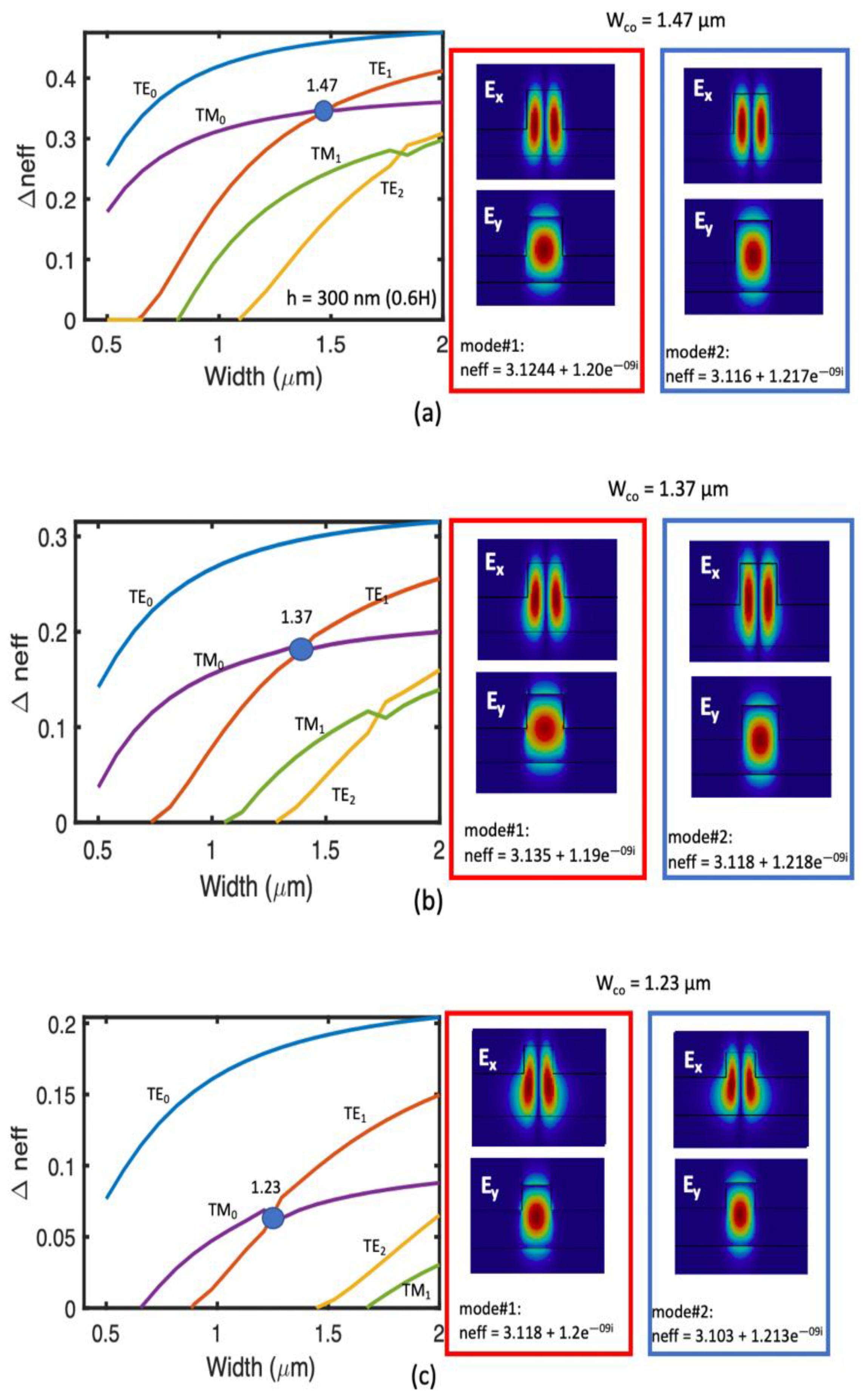
Figure 2a–c shows the Δn
eff for the SOI ridge waveguides for different etch depths for oxide-cladded ridge waveguide without any sidewall angle as the width of core silicon (W
co) varies from 0.5 μm to 3 μm. The mode hybridization between TM
0 and TE
1 is observed at silicon waveguide widths (W
co = W
h) of 1.47μm, 1.37 μm, and 1.23 μm for the ridges with etch-depths of 0.6 H, 0.5 H, and 0.4 H, respectively. It can be seen that W
h gets narrower when the waveguide etch-depth is reduced. As the latter is reduced from 0.6 H to 0.4 H, the mode hybridization region shifts from W
h = 1.47 μm to 1.23 μm. The simulation shows no significant change in the mode hybridization width (W
h) due to vertical asymmetry introduced by asymmetric cladding and angled sidewalls.
2.2. Taper Design for Efficient Mode Conversion
Due to mode hybridization at W
h, mode conversion between TM
0 and TE
1 will occur when light propagates along an adiabatic taper if its end widths W
1 and W
2 satisfy the condition: W
1 < W
h < W
2. In our design, the taper end width is chosen as W
1 = 1 μm and W
2 = 2 μm (
Figure 3). This will satisfy the mode conversion condition for a ridge waveguide with all the selected etch depths (W
1 = 1 μm < W
h = [1.47 μm, 1.37 μm, 1.23 μm] < W
2 = 2 μm). For TM-type PICs, where low loss TM
0 tapers are desired, mode conversion is harmful and causes unwanted losses. One of the simplest methods to avoid such unwanted mode conversion is to design tapers whose end widths are either (W
1, W
2) < W
h or (W
1, W
2) > W
h. However, if some design requirements put constraints on the end widths (W
1 < W
h < W
2), ultra-short non-adiabatic tapers should be implemented to preserve the TM fundamental mode.
An Eigen-Mode-Expansion method (EME-Ansys Lumerical) is used to simulate the mode conversion efficiency as the taper length (Ltp) increases. For scanning length in a very large range, the EME algorithm is very efficient compared to Finite-Difference-Time-Domain solver (FDTD). The simulations are performed for three different ridge heights under three different process conditions. The beam propagation simulation is also done in 3D FDTD to visualize the light propagation along the taper. For beam propagation simulation in FDTD, the same taper lengths of 200 μm (adiabatic) and 10 μm (TM-preserving) are chosen for different process conditions, and conversion ratios obtained are shown as well. The difference between EME and FDTD algorithm in determining the conversion efficiency is only 0.35%. The results are as follows:
2.2.1. (0.6. H) Ridge Waveguide (Ridge Height > Slab Height)
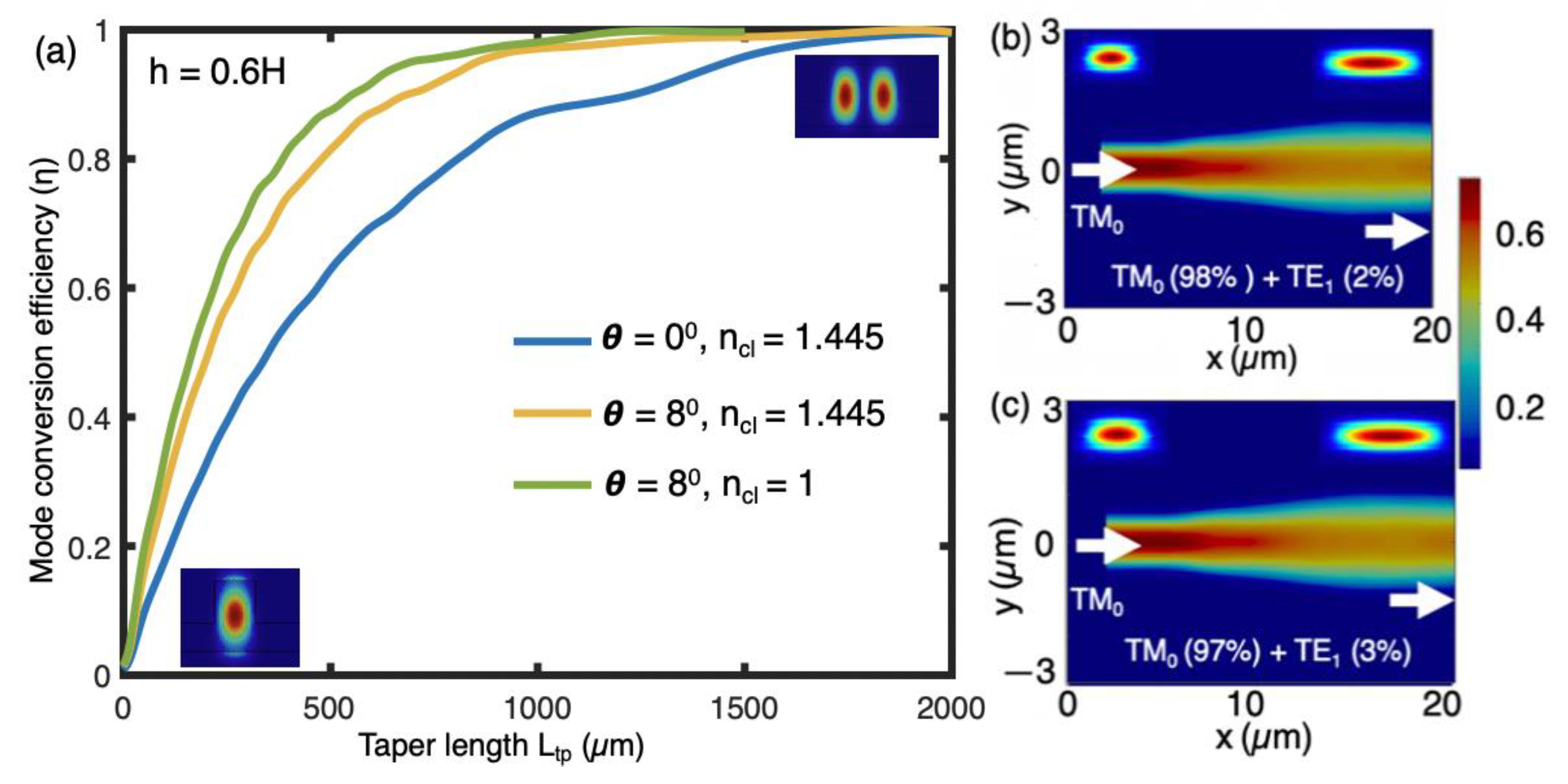
We start our analysis with a deeply etched ridge waveguide. The ridge height is 300 nm (0.6 H), corresponding to a slab height of 200 nm.
Figure 4 shows mode conversion efficiencies when the TM
0 mode is launched and coupled to the TE
1 mode. The TM
0 mode propagates along the adiabatic taper with a start and end widths of W
1 = 1 μm and W
2 = 2 μm, respectively. The simulations are performed for angled sidewalls and different top cladding conditions. From
Figure 4, one can realize very highly efficient tapers for TM
0 to TE
1 mode conversion with ~100% conversion efficiency by appropriately selecting L
tp. The L
tp required for mode conversion is observed to be strongly dependent on the process asymmetries related to the angled sidewalls and cladding material.
Under an ideal rectangular waveguide with symmetric cladding (SiO2), a taper length of 1820 μm is required for the complete mode conversion. However, when angled sidewalls are accounted for, the size is reduced to 1600 μm. This enhanced mode hybridization corresponds to a 12% reduction in taper length. Alternatively, when an air top cladding and sidewall angle are simultaneously present, the length for 100% mode conversion is reduced to 1110 μm. This corresponds to a total reduction of 39%, which is very significant compared to an ideal case.
It is important to note that mode conversion for SiO
2-cladding waveguide can be significantly reduced by choosing ultra-short taper lengths. From
Figure 4, the optimum length is 10 μm, for which the conversion efficiency is very low. For this taper length, the TM
0 mode preserving ability is highest, i.e., 98%, see FDTD (Finite-Difference Time-Domain) simulation in
Figure 4b). Since it is not possible to avoid angled sidewalls, it must be considered when designing low-loss TM tapers.
Figure 4c shows the transmission efficiency assuming a sidewall angle of 8
0. The drop-in efficiency due to angled sidewalls is only 1%, which is acceptable.
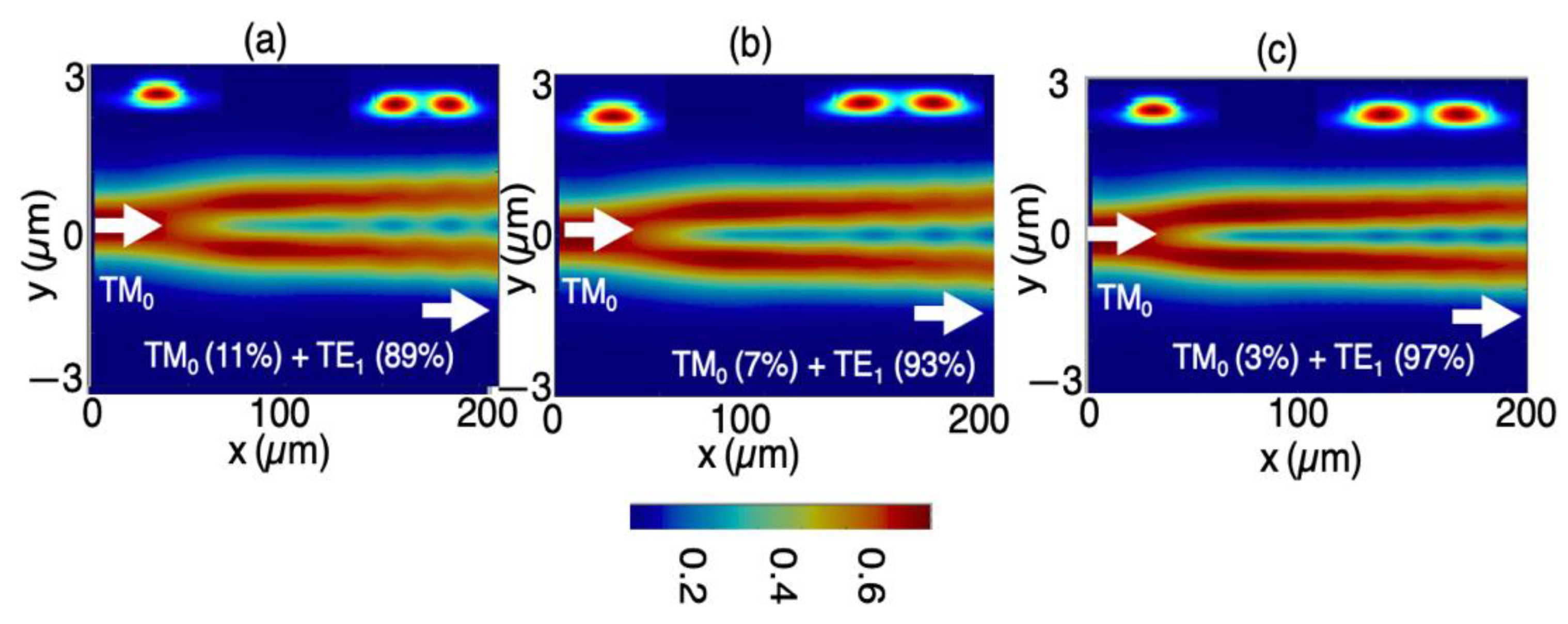
Figure 5 shows FDTD simulation along an adiabatic taper of length 200 μm when the launched mode is TM
0.
Figure 5a,b are shown for SiO
2 cladding with 0
0 and 8
0 sidewall angles, respectively, while
Figure 5c is shown for angled air-cladding waveguide. As predicted, the conversion efficiency increases with process asymmetries of the angled sidewalls and air-top cladding.
2.2.2. (0.5. H) Ridge Waveguide (Ridge Height = Slab Height)
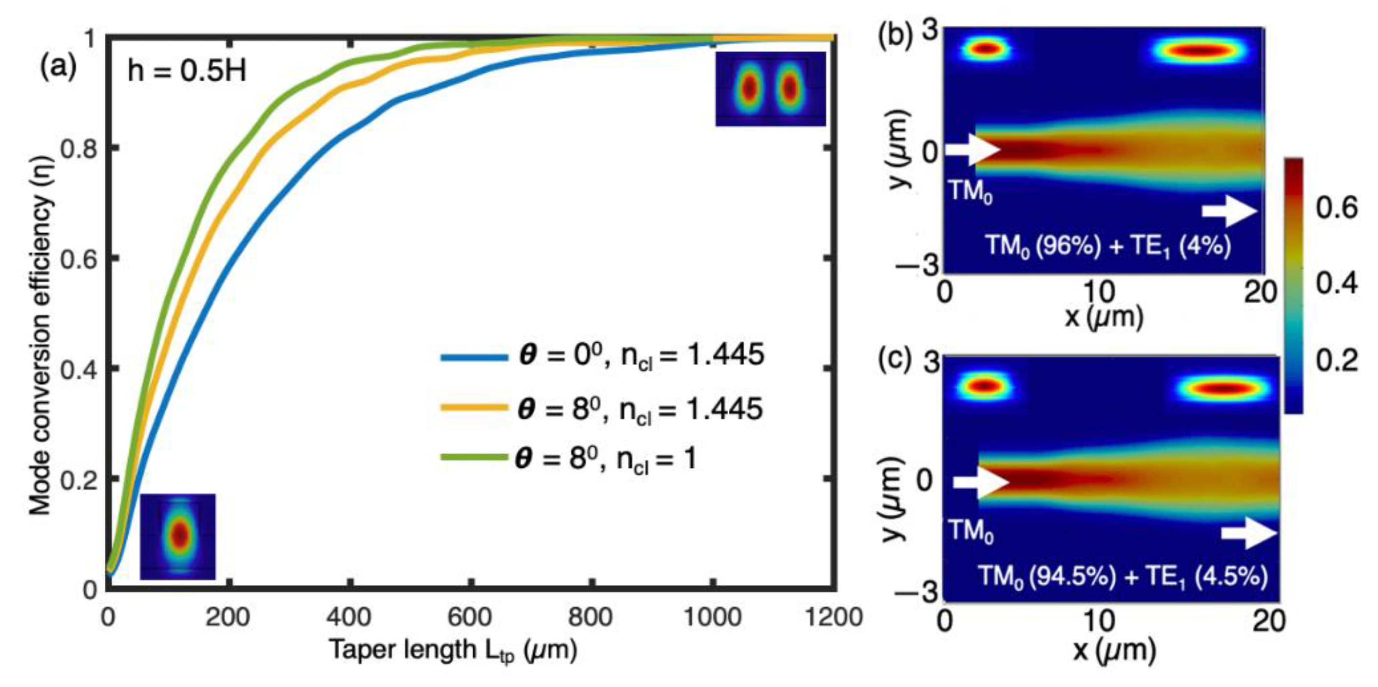
The etch-depth of the ridge waveguide is now reduced and made equal to slab height. In this case, both are equal to 250 nm. We observe a substantial increase in mode conversion efficiency as the ridge height is reduced. From
Figure 6, even for an ideal case with no sidewalls and symmetric SiO
2 cladding, the taper length for an efficient mode conversion is 985 μm. With angled sidewalls, the required L
tp is 750 μm, representing a 25% reduction in the overall length. Finally, when angled sidewalls and air-cladding are considered, the corresponding L
tp for mode conversion is 655 μm, which corresponds to a 33.5% reduction compared to an ideal case. When compared with deeply etched ridge waveguide, the effect of angled sidewalls is more pronounced. Since it is not possible to fabricate waveguides without sidewalls, the maximum efficiency is 94.5% for low-loss TM tapers for the sidewall angle of 8
0. For TM polarization preserving taper,
Figure 6b and 6c show FDTD propagation in an ultra-short L
tp = 10 μm for sidewall angles of θ = 0
0 and θ = 8
0, respectively.
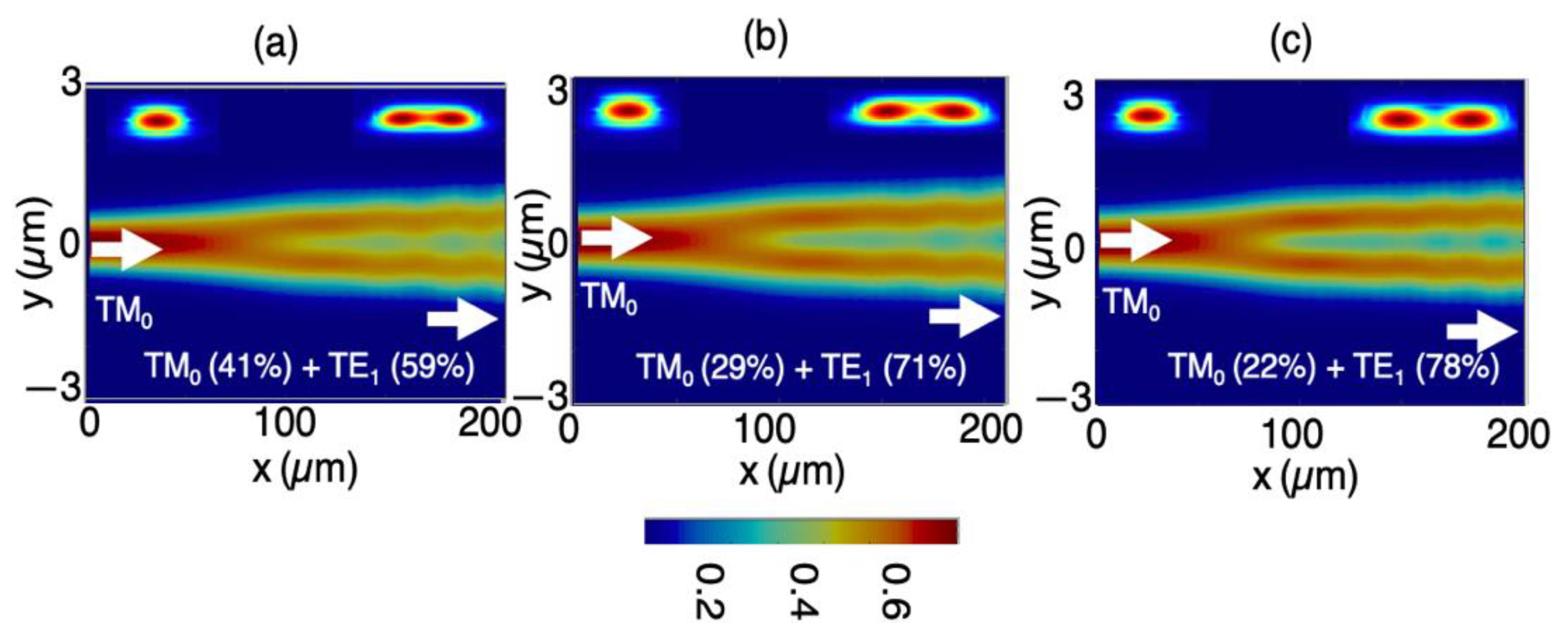
Figure 7 shows the light propagation along an adiabatic L
tp = 200 μm taper, similar to
Figure 5 but for 0.5 H etch-depth. Compared to
Figure 5, an increase in mode conversion efficiency for the same taper length is observed. It is evident that mode conversion in a tapered ridge waveguide is strongly dependent on etching depth. In a deeply etched waveguide, even when maximum asymmetry due to angled sidewalls and air top cladding is accounted, the conversion is only 56%, whereas, for a 0.5 H waveguide, it is 78%. Therefore, process parameters play an important role in mode conversion, and they must be accounted for in the PIC circuit design. Furthermore, a small change in the etch depth can cause a significant difference in the mode conversion.
2.2.3. (0.4. H) Ridge Waveguide (Ridge Height < Slab Height)
We finally consider a case of a low etched ridge waveguide in which ridge height is less than slab height. As seen from the 0.5 H waveguide analysis, the mode conversion efficiency increases as the etch-depth is reduced. For a low etched ridge waveguide, the mode conversion efficiency is maximum. It is not possible to further reduce the etch depth to enhance efficiency. Reducing the etch depth below certain limits causes TM fundamental mode to become leaky, and it is not well supported in the waveguide. However, it is still possible to increase the mode conversion efficiency and reduce the taper length requirement by accounting for enhanced mode hybridization due to angled sidewalls and asymmetric cladding. As depicted in
Figure 8, a 100% conversion efficiency between TM
0 and TE
1 mode is obtained at a taper length of 440 μm for an ideal case. The taper length is only 376 μm when the waveguide is modeled with a sidewall angle of 8
0. When both angled sidewalls and upper air cladding are considered, the size reduces to 277 μm. Additionally, low etch depth waveguides are reported to show lower propagation loss [
37]. This is due to a reduction in the optical mode interaction with the ridge sidewall.
Since in a low etch-depth ridge waveguide, very strong mode conversion is observed, it is not recommended to design an ultra-short taper to preserve the TM mode.
Figure 8 shows the light propagation in a taper with length L
tp = 10 μm. Even for an ideal case without any sidewall angle, the TM mode is maintained with only 85% efficiency. This efficiency further reduces to 83% when modeled with sidewalls.
Figure 9 shows FDTD beam propagation results along the designed taper with L
tp = 200 μm. A considerable increase in mode conversion efficiency is observed as expected compared to the deeply etched ridge waveguide (see
Figure 5).
Table 1 summarizes the important results for all the cases. It is concluded that, for efficient mode conversion, taper length can be significantly reduced by choosing the optimum process parameters. For a 100% mode conversion, we showed that an 1820 μm length taper could be reduced to a length of 277 μm by using a small ridge height and by considering angled sidewalls in an air clad waveguide. This corresponds to a total of 1540 μm (84.7%) decreases in the overall footprint. Even though an ultra-short taper successfully suppresses unwanted mode conversion, the TM
0 mode preserving efficiency is greatly improved if designed with a high etch-depth ridge waveguide.
3. Discussion
The insertion loss (IL) of a photonic device is defined as:
where P
in indicates input optical power and P
out indicates output optical power. In addition to surface roughness, the main loss mechanism in these devices is the presence and excitation of unwanted optical modes. In the case of TM to TE
1 mode converter, the percentage of TM mode in the output power contributes towards loss. Therefore, Equation (2) can be modified as:
Similarly, for a TM taper, the excitation of unwanted TE
1 mode is the main source of the loss. The insertion loss of the TM preserving taper can be defined as:
Therefore, the best low-loss configuration for the mode conversion is the air cladding with a partial etch of 0.4 H (0.176 dB), whereas for the TM preserving taper is the case of symmetric cladding with a ridge height of 0.6 H (0.084 dB). Here we have assumed an rms sidewall roughness of 3 nm.
Mode converters based on mode hybridization in adiabatic tapers are highly tolerant to fabrication tolerance. This is because irrespective of fabrication deviation in width, the mode hybridization width is always found along the taper. However, if the input width (W
1) is too close to the mode hybridization width (W
h), the device is more prone to fabrication variations. Along with width variation, there is also a possibility of thickness variation and changes in the sidewall angle. We study the effect of thickness and changes in sidewall angle (see
Figure 10). From this figure, it can be seen that the decrease in the ridge height slightly improves the mode conversion efficiency. Similarly, the increase in sidewall angle had a similar effect on the efficiency. However, fabrication variation does not cause much difference in the performance.

