Featured Application
Nondestructive functional imaging of bulk specimens by soft X-ray emission electron microscopy.
Abstract
Elemental and chemical state maps of p/n-controlled SrB6 bulk specimens are presented by using a soft X-ray emission spectroscopy electron microscope. Those bulk specimens were obtained by sintering powder specimens, prepared by the molten-salt method with different compositions of initial materials. A Sr-map, a chemical shift map of B K-emission, and the spectra of characteristic regions of those materials were compared. It was observed that a local Sr deficiency caused a local hole-doped region, confirmed by a chemical shift in the B K-emission spectrum. n-type SrB6 was rather homogeneous. On the other hand, the p-type SrB6 bulk specimen was a mixture of two different p-type regions. This mixed nature originated, presumably, from an uneven Sr content of SrB6 particles prepared by the molten-salt method using a Sr-deficient starting material. A separation process of the two types of materials will realize a high-quality homogeneous p-type SrB6 bulk specimens.
1. Introduction
Recent developments in new functional materials, with the help of theoretical simulations and data science, could accelerate practical applications of these new functional materials. For progressing those practical applications, not only improved and effective material processing methods, but also quick feedback of the evaluated results of the structure, composition, and chemical state of new products are necessary. Dedicated transmission electron microscope (TEM) is a powerful candidate for evaluating the structure and chemical characteristics of materials, with a nanometer-scale spatial resolution [1,2,3,4]. However, it is a destructive inspection process due to a necessity of thin specimens of about tens of nanometers for transmission experiments. For a nondestructive inspection process with a high spatial resolution, evaluations based on scanning electron microscopy are useful. A soft X-ray emission spectroscopy (SXES) instrument, combined with a scanning electron microscope (SEM) and/or an electron probe microanalyzer (EPMA) can realize a nondestructive inspection process of the chemical state of materials, with a spatial resolution of about 1 µm or better [5,6,7]. If this occurs, SXES microscopy can make a quick feedback loop of the evaluated results of new products for materials processing.
The chemical state analysis of boron is a topical issue in materials science. Boron forms four allotropes of α,β-rhombohedral boron and α,β-tetragonal boron. These materials have a three-dimensional network of boron clusters. α-rhombohedral boron is expected to be a superconductor by electron doping [8,9]. Boron compounds also express interesting characteristics as metals, semiconductors, insulators, and superconductors [10,11,12]. In addition, boron is one of the key chemical species as a fine additive element in the production of functional tuff steel, magnetic materials, the formation of fundamental switches for large integrated circuits, medical applications, etc. [13,14,15,16]
The alkaline-earth hexaborides CaB6, SrB6, and BaB6 are candidate materials for thermoelectric conversion because of their large Seebeck coefficients and electrical conductivities [17,18]. Each material is composed of a three-dimensional network of B6 octagonal clusters, placed at each corner of a cubic unit cell, and an incorporated alkaline-earth metal atom at the body-center position of the unit cell. The metal atom can transfer two valence electrons to the B6 cluster network, resulting in an n-type semiconductor. For realizing a thermoelectric device using B6 cluster network materials, a p-type semiconductor is necessary. As Na atoms only have one valence electron, Na substitution to the Ca site of CaB6 (Na-doped CaB6) is a hole-doping to the B6 cluster network, causing a p-type semiconductor as a bulk [19]. This p-type Na-doped CaB6 was evaluated by using a commercial SXES-EPMA instrument, which reported an inhomogeneous charge distribution due to a compositional fluctuation in the bulk [20]. p/n-type controlled CaB6 bulk materials, prepared by the molten-salt method with starting materials containing different compositional ratios of Ca and B, were also examined by SXES-EPMA. It was revealed that the produced p-type bulk CaB6 specimen included locally n-type regions [21].
In this report, nondestructive chemical state evaluations of p/n-controlled SrB6 bulk specimens are presented. Two-dimensional spectral mapping of the soft X-ray emission spectra of these materials gives information of elemental inhomogeneity, and the related hole-doping nature appears as a chemical shift in the spectra of the material.
2. Methods and Materials
2.1. Chemical State Information by SXES
Electron-beam-induced X-ray emission was used for elemental analysis by using an X-ray energy dispersive spectroscopy (EDS) instrument, and elemental and partial chemical analyses were performed using an EPMA. Among those X-rays, X-rays due to transitions from valence bands (bonding state) to inner-shell levels, usually lower than 1 keV, have information about the chemical bonding states of elements. Recent soft X-ray emission spectrometry using gratings, which was first developed for TEM [22,23,24] and then transferred to SEM and EPMA [5,6,7], has an energy resolution better than 1 eV, which is about two orders better than that of EDS and allowed us to obtain chemical bonding information by using X-ray emission. Another spectrometer system for soft X-rays is under examination [25].
Figure 1 shows the electronic transitions in a material caused by electron beam irradiation. Firstly, incident electrons excite electrons, a and b. This automatically causes energy losses of the incident electrons, which is the physical quantity to be measured in electron-energy-loss spectroscopy in TEM. The excited material quickly returns to the ground state. In the de-excitation process, downward electronic transitions of c and d to inner-shell core-hole states, which were created by the excitation process b, occur by accompanying X-ray emissions under a dipole-selection rule condition. Both emissions of c and d in Figure 1 are used in elemental analysis. However, only the X-ray emissions caused by the transition c includes information about the energy distribution of bonding electrons, the density of states of valence bands (VB). Thus, X-rays due to transitions c are a sensitive tool for chemical state analysis. As the energy spread of VB is smaller than 10 eV, an energy resolution better than 1 eV is necessary for obtaining information of chemical bonding states by SXES.
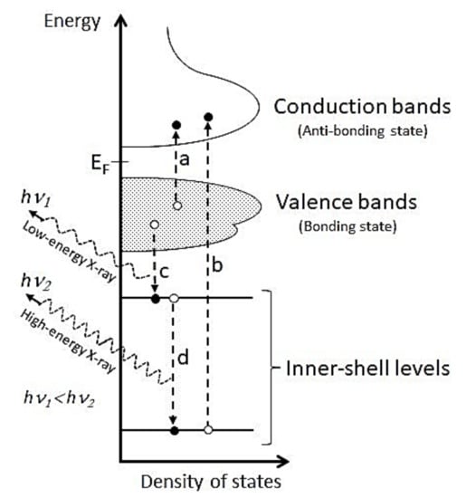
Figure 1.
Electronic transitions related to electron energy-loss spectroscopy, a and b, and X-ray emission spectroscopy, c and d. Only X-ray emissions due to transitions c include a chemical bonding information.
Figure 2a shows a schematic figure of the SXES mapping system used. The SXES system (JEOL SS-94000SXES), which is composed of varied-line-spacing gratings (aberration-corrected gratings) and a CCD detector, was attached to an EPMA (JEOL JXA-8230). The distance from the specimen to the detector was about 50 cm. The combination of the two VLS gratings of JS50XL and JS200N covers 50–210 eV for the 1st-order diffraction lines, and 100–420 eV for the 2nd-order diffraction lines [7]. The energy resolution of about 0.2 eV was realized for the 1st-order Al L-emission at about 73 eV. Figure 2b shows the 1st-order B K-emission (corresponds to transition c in Figure 1) spectra of pure boron (β-rhombohedral boron, β-r-B), CaB6, AlB2, and hexagonal-BN (h-BN). N-K(2) in the h-BN spectrum is the 2nd-order line of N K-emission, which shows a larger intensity than B K-emission because the bonding orbital is dominated by an N-orbital component, owing to its lower energy than that of B. The peak energy positions (vertical arrows) and the shoulder structures (vertical lines) of the B K of these materials are different from each other, reflecting different chemical bonding states owing to different crystal structures. By using a high energy resolution, elemental and chemical state analyses and those mappings are possible [5,6,7,26,27,28,29,30]. The emission due to the process d is also affected by the chemical state of the materials [31,32].
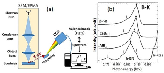
Figure 2.
(a) SXES-EPMA system used. The SXES spectrometer is composed of gratings and a CCD detector, which enables a parallel detection in a certain energy range. (b) B K-emission spectra of pure boron and boron compounds. Peak energy position (arrows) and shoulder structures (line) are different each other, reflecting different chemical bonding states owing to different crystal structures.
2.2. Preparation of p/n-Controlled SrB6 Bulk Specimens
The molten-salt method reported for low-temperature synthesis of CaB6 powders [33] was applied for the present preparation of SrB6 specimens. The reaction used is as follows: SrCl2 + 6NaBH4 → SrB6 + 2NaCL +12H2 + 4Na. Three SrB6 materials were prepared by using different starting materials, with compositions of: Sr:B = 1:1 (Sr excess), 1:6 (stoichiometry), and 1:12 (Sr-deficient).
Well-mixed starting materials of SrCl2 and NaBH4 were placed in crucibles of stainless steel, heated up to 1073 K and maintained for 10 h under an Ar atmosphere. The produced materials were washed with acid and water to remove impurities other than SrB6. The obtained powder materials were sintered at 1800 K and 50 MPa for 20 min by the pulsed electric current sintering method, and bulk specimens were obtained. The crystallinity of those specimens was examined and confirmed as SrB6 crystalline specimens by X-ray diffraction. From the measurements of the Seebeck coefficient, the obtained specimens from the starting materials of Sr:B = 1:1 (Sr excess) and 1:6 (stoichiometry) were n-type semiconductors. On the other hand, the material started with Sr:B = 1:12 (Sr-deficient) was a p-type semiconductor.
3. Results
3.1. Observation of p/n-Controlled SrB6 by Backscattering Electron
Figure 3 shows backscattered electron (BSE) images of sintered bulk specimens of the n-type, prepared with Sr:B = 1:1 and 1:6, and p-type, prepared with Sr:B = 1:12 (Sr-deficient composition). It was observed that the images of the n-type specimen are dominated by bright and rather homogeneous regions. On the other hand, the BSE image of the p-type specimen in Figure 3c is apparently inhomogeneous; it shows a co-existence of bright and dark regions. The BSE image shows a larger intensity for an area with a larger averaged atomic number Z. Thus, the dark regions in Figure 3c could be understood as apparently Sr-deficient regions of 1 μm or much smaller in size. A Sr-deficient, hole-doping, SrB6 specimen could be a p-type semiconductor. However, the BSE image cannot give us chemical state information. Thus, the following SXES investigation is important to judge the physical properties of these materials.
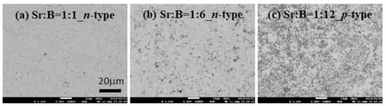
Figure 3.
Back-scattering electron images of sintered SrB6 bulk specimens. The image of the p-type specimen is apparently inhomogeneous. Dark contrast regions could be Sr-deficient regions. (a) Sr:B = 1:1_n-type; (b) Sr:B = 1:6_n-type;.(c) Sr:B = 1:12_p-type.
3.2. SXES Mapping of n-Type SrB6
Figure 4a shows a BSE image of a piece of an n-type SrB6 specimen prepared with a Sr-excess composition of Sr:B = 1:1. A spectral mapping procedure was performed with a probe current of 40 nA at an accelerating voltage of 5 kV. The specimen area in Figure 4a was divided into 20 × 15 pixels of about 0.6 µm pitch. Electrons of 5 keV, impinged on the SrB6 surface, spread out inside the material via inelastic scattering of about 0.22 μm in diameter, which was evaluated by using Reed’s equation [34]. The size, which corresponds to the lateral spatial resolution of the SXES measurement, is smaller than the pixel size of 0.6 μm. SXES spectra were obtained from each pixel with an acquisition time of 20 s. Figure 4b shows a map of the Sr Mζ-emission intensity of each pixel divided by an averaged value of the Sr Mζ intensity of the area examined. The positions of relatively Sr-deficient areas with blue color in Figure 4b are a little different from those which appear in the dark contrast area in the BSE image in Figure 4a. This could be due to a smaller information depth of the BSE image than that of the X-ray emission (electron probe penetration depth) [35]. The raw spectra of the squared four-pixel areas A and B are shown in Figure 4c, which show a sufficient signal -o-noise ratio. Each spectrum shows B K-emission intensity due to transitions from VB to K-shell (1s), which corresponds to c in Figure 1, and Sr Mζ-emission intensity due to transitions from N2,3-shell (4p) to M4,5-shell (3d), which corresponds to Figure 1d [36,37]. These spectra intensities were normalized by the maximum intensity of B K-emission. Although the area B exhibits a slightly smaller Sr content than that of A in Figure 4b, the intensities of Sr Mζ-emission of those areas in Figure 4c are almost the same, suggesting the inhomogeneity was small.
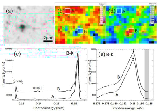
Figure 4.
(a) BSI image, (b) Sr Mζ-emission intensity map, (c) spectra of areas A and B in (b), (d) chemical shift map of B K-emission, and (e) B K-emission spectra of A and B in (d).
When the amount of Sr in an area is deficient, the amount of the valence charge of the B6 cluster network of the area should be deficient (hole-doped). This causes a shift in B 1s-level (chemical shift) to a larger binding energy side. This can be observed as a shift in the B K-emission spectrum to the larger energy side as already reported for Na-doped CaB6 [20] and Ca-deficient n-type CaB6 [21]. For making a chemical shift map, monitoring of the spectrum intensity from 187 to 188 eV at the right-hand side of the spectrum (which corresponds to the top of VB) is useful [20,21]. The map of the intensity of 187–188 eV is shown in Figure 4d, in which the intensity of each pixel is divided by the averaged value of the intensities of all pixels. When the chemical shift to the higher energy side is large, the intensity in Figure 4d is large. It should be noted that larger intensity areas in Figure 4d correspond with smaller Sr-Mζ intensity areas in Figure 4c. The B K-emission spectra of areas A and B are shown in Figure 4e. The gray band of 187–188 eV is the energy window used for making Figure 4d. Although the Sr Mζ intensity of the areas are almost the same, the peak of the spectrum B shows a shift to the larger energy side of about 0.1 eV and a slightly longer tailing to the higher energy side, which is a small change in intensity distribution. These could be due to a hole-doping caused by a small Sr deficiency as observed in Figure 4b. The area could be a hole-doped p-type region embedded in a n-type bulk specimen. This local inhomogeneity of Sr could be due to an inhomogeneity in the starting materials.
3.3. SXES Mapping of p-Type SrB6
Figure 5a shows a BSE image of a p-type SrB6 bulk specimen prepared with an Sr-deficient composition of Sr:B = 1:12. As the contrast of BSI depends on the atomic number, the complex white and black contrast in the BSI image suggests an inhomogeneous distribution of Sr. Figure 5b shows an intensity map of Sr Mζ-emission divided by an averaged value. The spectra (raw data) of areas A and B are shown in Figure 5c. The spectrum B shows a largely decreased Sr-Mζ intensity than that of A.
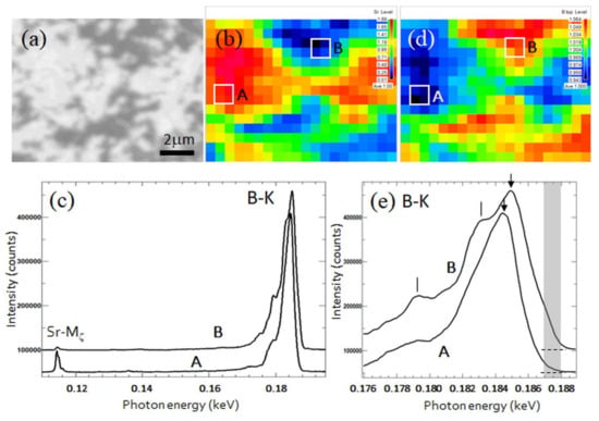
Figure 5.
(a) BSI image, (b) spectra of areas A and B in (c), (c) Sr-Mζ-emission intensity map, (d) chemical shift map of B K-emission, (e) B K-emission spectra of areas of A and B in (d).
Figure 5d is a chemical shift map prepared using the same manner for that in Figure 4d. It is clearly seen that the B K-emission spectra of Sr-deficient regions, dark areas in Figure 5b, show a chemical shift to the larger energy side, as seen in bright color in Figure 5d. The enlarged B K-emission spectra of areas A and B are shown in Figure 5e. The gray band of 187–188 eV is the energy window used to make Figure 5d. The spectrum of the area B with a large Sr-deficient region shows not only a shift of the B K-emission peak position to the larger energy side, but also an additional shoulder structure, indicated by vertical lines. This means that the area could have a crystal structure comprising largely deformed SrB6, or a structure different from that of SrB6. Such shoulder structures of B K-emission spectra were also observed in Na-doped [20] and Ca-deficient [21] p-type CaB6 bulk specimens. A different crystal structure of boron can show a different peak energy in B K-emission as already shown in Figure 2b. Thus, the area B could be a p-type region, but the amount of the peak shift cannot be explained by the hole-doping only. On the other hand, the intensity profile of spectrum A in Figure 5e is similar to those in Figure 4e. The Sr-Mζ intensity of the area A in Figure 5c is smaller than that of the spectrum of area A in Figure 4c. Furthermore, the peak position of the B K-spectrum shifted slightly to the larger energy side about 0.1 eV than that of A in Figure 4e. Thus, area A could be a hole-doped p-type region having the SrB6 structure. Thus, the area A should be representative of p-type SrB6 aimed for in the specimen preparation.
4. Discussion
The present experimental results of SXES mappings showed that the present n-type SrB6 bulk specimen was almost uniform except for a local fluctuation in Sr content. On the other hand, p-type bulk specimen was apparently not uniform. The specimen was composed of two p-type regions. One was the region containing a small amount of Sr -deficiency and having the SrB6 type crystal structure, which was the material aimed for in specimen preparation. The other was the region with a large amount of Sr deficiency, which had a largely deformed SrB6 structure or a differently structured boron material. This could be the result of an Sr-deficient composition of starting material used for the molten-salt method. From the experimental results, the fine SrB6 particles prepared by molten-salt method may have had a large dispersion of Sr content. Therefore, any process to separate the two types of materials, a centrifugal process for example, before the sintering process would be effective to prepare a uniform p-type SrB6 bulk specimen.
5. Conclusions
Homogeneity of composition and the related chemical states of p/n-controlled SrB6 bulk specimens were examined by using an SXES microscope. It was revealed that the present p-type bulk specimen is composed of two types of regions. Those regions showed differences in the amount of Sr content and the crystal lattice. Based on the results, an additional process was proposed to separate the two materials prepared by the molten-salt method. Therefore, we presented that the nondestructive inspection process of bulk materials using a SXES microscope can realize quick feedback of the results of chemical state analyses of the material to the production process and contribute to an improvement in the specimen preparation process.
Author Contributions
Specimen preparation and characterization, M.T. (Masatoshi Takeda); soft X-ray emission experiment, M.T. (Masami Terauchi); SXES data analysis and discussion, M.T. (Masami Terauchi) and Y.K.S.; writing original draft preparation and funding acquisition, M.T. (Masami Terauchi) and M.T. (Masatoshi Takeda). All authors have read and agreed to the published version of the manuscript.
Funding
This research was funded by the Research Program of the Dynamic Alliance for Open Innovation Bridging Human, Environment and Materials of the Ministry of Education, Culture, Sports, Science and Technology, Japan, and the Network Joint Research Centre for Materials and Devices; Japan Society for the Promotion of Science KAKENHI (grant numbers 15H02299; 19K21838).
Institutional Review Board Statement
Not applicable.
Informed Consent Statement
Not applicable.
Acknowledgments
The authors thank M. Ageishi of the Institute of Multidisciplinary Research for Advanced Materials, Tohoku University, for his skillful technical assistance.
Conflicts of Interest
The authors declare no conflict of interest.
References
- Kimoto, K.; Xie, R.J.; Matsui, Y.; Ishizuka, K.; Hirosaki, N. Direct observation of single dopant atom in light-emitting phosphor of β-SiAlON:Eu2+. Appl. Phys. Lett. 2009, 94, 041908. [Google Scholar] [CrossRef]
- Sato, Y.; Terauchi, M.; Adachi, K. High energy-resolution electron energy-loss spectroscopy study on the near-infrared scattering mechanism of Cs0.33WO3 crystals and nanoparticles. J. Appl. Phys. 2012, 112, 074308. [Google Scholar] [CrossRef]
- Krivanek, O.L.; Lovejoy, T.C.; Dellby, N.; Aoki, T.; Carpenter, R.W.; Rez, P.; Soignard, E.; Zhu, J.; Batson, P.E.; Lagos, M.J.; et al. Vibrational spectroscopy in the electron microscope. Nature 2014, 514, 209–212. [Google Scholar] [CrossRef] [PubMed]
- Tsuda, K.; Tanaka, M. Direct observation of the symmetry breaking of the nanometer-scale local structure in the paraelectric cubic phase of BaTiO3 using convergent-beam electron diffraction. Appl. Phys. Express 2016, 9, 071501. [Google Scholar] [CrossRef]
- Takahashi, H.; Handa, N.; Murano, T.; Terauchi, M.; Koike, M.; Kawachi, T.; Imazono, T.; Hasegawa, N.; Koeda, M.; Nagano, T.; et al. Chemical State Mapping via Soft X-rays using a Wavelength Dispersive Soft X-ray Emission Spectrometer with High Energy Resolution. Microsc. Microanal. 2013, 19 (Suppl. S2), 1258–1259. [Google Scholar] [CrossRef] [Green Version]
- Terauchi, M.; Koshiya, S.; Satoh, F.; Takahashi, H.; Handa, N.; Murano, T.; Koike, M.; Imazono, T.; Koeda, M.; Nagano, T.; et al. Chemical state information of bulk specimens obtained by SEM-based soft-x-ray emission spectrometry. Microsc. Microanal. 2014, 20, 692–697. [Google Scholar] [CrossRef]
- Takahashi, H.; Murano, T.; Takakura, M.; Asahina, S.; Terauchi, M.; Koike, M.; Imazono, T.; Koeda, M.; Nagano, T. Development of soft X-ray emission spectrometer for EPMA/SEM and its application. IOP Conf. Ser. Mater. Sci. Eng. 2016, 109, 012017. [Google Scholar] [CrossRef] [Green Version]
- Gunji, S.; Kaminura, H. First-principle study on metal-doped icosahedral B12 solids. Phys. Rev. B 1996, 54, 13665–13673. [Google Scholar] [CrossRef]
- Nagatochi, T.; Hyodo, H.; Sumiyoshi, A.; Soga, K.; Sato, Y.; Terauchi, M.; Esaka, F.; Kimura, K. Superconductivity in Li-doped α-rhombohedral boron. Phys. Rev. B 2011, 83, 184507. [Google Scholar] [CrossRef]
- Etourneau, J.; Hagenmuller, P. Structure and physical features of the rare-earth borides. Philos. Mag. B 1985, 52, 589–610. [Google Scholar] [CrossRef]
- Albert, B.; Hillebrecht, H. Boron: Elementary Challenge for Experimenters and Theoreticians. Angew. Chem. Int. Ed. 2009, 48, 8640–8668. [Google Scholar] [CrossRef]
- Nagamatsu, J.; Nakagawa, N.; Muranaka, T.; Zenitani, Y.; Akimitsu, J. Superconductivity at 39 K in magnesium diboride. Nature 2001, 40, 63–64. [Google Scholar] [CrossRef] [PubMed]
- Haga, J.; Mizui, N.; Nagamichi, T.; Okamoto, A. Effect of Boron on Mechanical Properties and Recrystallization Behavior of Ti-added Ultra-low Carbon Cold-rolled Steel Sheets. ISIJ Int. 1998, 38, 580–586. [Google Scholar] [CrossRef]
- Scheifers, J.P.; Zhang, Y.; Fokwa, B.P.T. Boron: Enabling Exciting Metal-Rich Structures and Magnetic Properties. Acc. Chem. Res. 2017, 50, 2317–2325. [Google Scholar] [CrossRef]
- Zhang, X.; Wang, B.; Huang, W.; Chen, Y.; Wang, G.; Zheng, L.; Zhu, W.; Bedzyk, M.J.; Zhang, W.; Medvedeva, J.E.; et al. Synergistic Boron Doping of Semiconductor and Dielectric Layers for High-Performance Metal Oxide Transistors: Interplay of Experiment and Theory. J. Am. Chem. Soc. 2018, 140, 12501–12510. [Google Scholar] [CrossRef] [PubMed]
- International Atomic Energy Agency. Current Status of Neutron Capture Therapy; International Atomic Energy Agency: Vienna, Austria, 2001. [Google Scholar]
- Takeda, M.; Fukuda, T.; Domingo, F.; Miura, T. Thermoelectric properties of some metal borides. J. Solid State Chem. 2004, 177, 471–475. [Google Scholar] [CrossRef]
- Takeda, M.; Terui, N.; Takahashi, N.; Ueda, N. Improvement of thermoelectric properties of alkaline-earth hexaborides. J. Solid State Chem. 2006, 179, 2823–2826. [Google Scholar] [CrossRef]
- Kuribayashi, H.; Makino, S.; Takeda, M. Synthesis and Characterization of p-type CaB6. Abstract of ISBB-18. In Proceedings of the 2014 IEEE International Symposium on Bioelectronics and Bioinformatics, Chung Li, Taiwan, 11–14 April 2014; p. 148. [Google Scholar]
- Terauchi, M.; Sato, Y. Chemical State Analyses by Soft X-ray Emission Spectroscopy. JEOL NEWS 2018, 53, 30–35. [Google Scholar]
- Terauchi, M.; Sato, Y.K.; Takeda, M. Chemical State Mapping of Bulk Materials by Electron Microscopy Based Soft X-ray Emission Spectroscopy. Mater. Jpn. 2021, 60, 341–346. [Google Scholar] [CrossRef]
- Terauchi, M.; Yamamoto, H.; Tanaka, M. Development of a sub-eV resolution soft-X-ray spectrometer for a transmission electron microscope. J. Electron Microscopy 2001, 50, 101–104. [Google Scholar] [CrossRef]
- Terauchi, M.; Kawana, M. Soft-X-ray emission spectroscopy based on TEM – Toward a total electronic structure analysis. Ultramicroscopy 2006, 106, 1069–1075. [Google Scholar] [CrossRef] [PubMed]
- Terauchi, M. Valence Electron Spectroscopy for Transmission Electron Microscopy. In Transmission Electron Microscopy Characterization of Nanomaterials, 1st ed.; Kumar, C.S.S.R., Ed.; Springer: Berlin/Heidelberg, Germany, 2014. [Google Scholar] [CrossRef]
- Yin, Z.; Rehanek, J.; Lochel, H.; Braig, C.; Buck, J.; Frisov, A.; Viefhaus, J.; Erko, A.; Techert, S. Highly efficient soft X-ray spectrometer based on a reflection zone platre for resonant inelastic X-ray scattering measurements. Opt. EXPRESS 2017, 25, 10984–10996. [Google Scholar] [CrossRef] [Green Version]
- Ishii, S.; Terauchi, M.; Sato, Y.; Tamura, N.; Aono, M.; Abe, H. Soft X-ray emission spectroscopy study of characteristic bonding states and its distribution of amorphous carbon-nitride (a-CNx) films. Microscopy 2018, 67, 244–249. [Google Scholar] [CrossRef] [PubMed] [Green Version]
- Terauchi, M.; Takahashi, H.; Takakura, M.; Murano, T.; Koshiya, S. Handbook of Soft X-ray Emission Spectra, 6th ed.; JEOL Ltd.: Tokyo, Japan, 2020; pp. 244–250. [Google Scholar]
- Kasada, R.; Ha, Y.; Higuchi, T.; Sakamoto, K. Chemical State Mapping of Degraded B4C Control Rod Investigated with Soft X-ray Emission Spectrometer in Electron Probe Micro-analysis. Sci. Rep. 2016, 6, 25700. [Google Scholar] [CrossRef] [PubMed] [Green Version]
- Mukai, K.; Kasada, R.; Yabuuchi, K.; Konishi, S.; Kim, J.H.; Nakamichi, M. Valence Electron and Chemical State Analysis of Be12M (M=Ti, V) Beryllides by Soft X-ray Emission Spectroscopy. ACS Appl. Energy Mater. 2019, 2, 2889–2895. [Google Scholar] [CrossRef] [Green Version]
- MacRae, C.M.; Pearce, M.A.; Wilson, N.C.; Torpy, A.; Glenn, M.A.; Russo, S.P. Soft X-ray and Cathodoluminescence Examination of a Tanzanian Graphite Deposit. Microsc. Microanal. 2020, 26, 814–820. [Google Scholar] [CrossRef]
- Terauchi, M.; Koshiya, S.; Kimoto, K. Information observed in Ti-Lα,β and Ti-Lℓ,η emission lines of Ti and its oxides. IOP Conf. Ser. Mater. Sci. Eng. 2018, 304, 012018. [Google Scholar] [CrossRef]
- Terauchi, M. Information of valence charge of 3d transition metal elements observed in L-emission spectra. Microscopy 2019, 68, 330–337. [Google Scholar] [CrossRef]
- Shi, L.; Gu, Y.; Chen, L.; Yang, Z.; Ma, J.; Qian, Y. Low Temperature Synthesis and Characterization of Cubic CaB6 Ultrafine powders. Chem. Lett. 2003, 32, 958–959. [Google Scholar] [CrossRef]
- Reed, S.J.B. Electron Microprobe Analysis, 2nd ed.; Cambridge University Press: Cambridge, UK, 1993; pp. 199–201. [Google Scholar]
- Niedrig, H.; Rau, E.I. Information depth and spatial resolution in BSE microtomography. Nucl. Instr. Meth. Phys. Res. B 1998, 142, 523–534. [Google Scholar] [CrossRef]
- Bearden, J.A. X-ray Wavelengths. Rev. Mod. Phys. 1967, 39, 78–124. [Google Scholar] [CrossRef]
- Zschornack, G. Handbook of X-ray Data, 1st ed.; Springer: Berlin/Heidelberg, Germany, 2007; p. 265. [Google Scholar]
Publisher’s Note: MDPI stays neutral with regard to jurisdictional claims in published maps and institutional affiliations. |
© 2021 by the authors. Licensee MDPI, Basel, Switzerland. This article is an open access article distributed under the terms and conditions of the Creative Commons Attribution (CC BY) license (https://creativecommons.org/licenses/by/4.0/).