Article

Tuning of Graphene-Based Optical Devices Operating in the Near-Infrared

by
Artem S. Vorobev
1,2,*,
Giuseppe Valerio Bianco
3,
Giovanni Bruno
3,
Antonella D’Orazio
1,
Liam O’Faolain
2,4 and
Marco Grande
1,*
1
Department of Electrical and Information Engineering, Politecnico di Bari, 4, 70126 Bari, Italy
2
Centre for Advanced Photonics and Process Analysis, Munster Technological University, T12 T66T Cork, Ireland
3
CNR-Nanotec, Department of Chemistry, University of Bari, Via Orabona, 4, 70123 Bari, Italy
4
Tyndall National Institute, T12 PX46 Cork, Ireland
*
Authors to whom correspondence should be addressed.
Appl. Sci. 2021, 11(18), 8367; https://doi.org/10.3390/app11188367
Submission received: 3 August 2021 / Revised: 31 August 2021 / Accepted: 7 September 2021 / Published: 9 September 2021
(This article belongs to the Special Issue Graphene-Based Microwave and Optical Devices)

Abstract

:
Graphene is a material with exceptional optical, electrical and physicochemical properties that can be combined with dielectric waveguides. To date, several optical devices based on graphene have been modeled and fabricated operating in the near-infrared range and showing excellent performance and broad application prospects. This paper covers the main aspects of the optical behaviour of graphene and its exploitation as electrodes in several device configurations. The work compares the reported optical devices focusing on the wavelength tuning, showing how it can vary from a few hundred up to a few thousand picometers in the wavelength range of interest. This work could help and lead the design of tunable optical devices with integrated graphene layers that operate in the NIR.

1. Introduction

Graphene, a two-dimensional (2D), semi-metallic material with a zero-band gap, has a unique band structure of a narrowing Dirac zone and a linear dispersion dependence [1,2,3], which makes it a promising material for devices due to its tunable and broadband optical properties. Graphene is a single layer of a graphite crystal with a single atomic layer structure of pure covalently bonded carbon atoms arranged in a hexagonal lattice structure. Each carbon atom has six electrons, which surround its nucleus (two in the inner shell and four in the outer electron shell). Three of these four electrons are bound with the nearest-neighbor atom electrons allowing the creation of strong chemical bonds that make graphene one of the strongest materials at the nanoscale. The other, unbound, electron in the outer electron shell of each carbon atom is delocalized across the whole graphene layer [4]. The band structure of a delocalized electron determines the conductivity of graphene. In this regard, there is no gap between the conduction band and the valence band, which allows us to consider it as a gapless semiconductor. By considering that the Fermi level of pure graphene is located at the point of intersection of the conduction band and the valence band (Dirac point), it can be considered as a metal with an empty valence band. The transition between the properties of a semiconductor and a metal can be controlled by adjusting the position of the Fermi level relative to the Dirac point, either with the help of chemical approaches, or with the help of the electric field effects. Since free electrons are tightly enclosed in one atomic layer, graphene has a very low density of states, especially when the electron energy is close to the Dirac point. Therefore, small changes in the carrier density can cause significant shifts in the Fermi energy, which change the rate of interband transitions and, consequently, the optical constant [5]. This effect can be achieved by introducing doping using electrical and/or chemical gating, which shifts the Fermi energy from the Dirac point and, in turn, changes the optical response of graphene [6]. This approach opens the possibility of easily tuning graphene from a “lossy-dielectric” behaviour to the “quasi-metallic” region, which can be used to implement modulators (based on electro-optical graphene optical behaviour, Mach–Zehnder interferometers, rings, switches and Zeno-based modulators) [7,8,9,10,11,12,13,14,15,16,17,18,19,20,21,22,23], resonators [24,25,26], or can be applied to a wide variety of devices that operate at a specific resonance and require wavelength tuning [27,28,29]. It should be noted that the use of this property of graphene is not limited only to the NIR range; in this regard, electro-optical graphene terahertz modulators can be noted [30,31,32]. The nonlinear photonics of graphene finds many applications, including spatial and spectral control of laser light, all-optical signal processing, ultrafast switching and probing, and frequency multiplication of the terahertz range [33,34,35,36,37,38]. Graphene is also an affordable means for implementing a saturable absorber (SA) [39,40,41,42,43].
It is worth noting that, in addition to graphene, 2D materials such as transition metal dichalcogenides (TMD), for example MoS2, WS2, MoSe2, ReS2, WSe2 and others [44,45,46], and black phosphorus [47,48,49,50], are gaining popularity, but TMDs show a band gap of about 1 to 2.5 eV (which corresponds to frequencies from NIR to visible), and the band gap of phosphorus is highly variable depending on the number of layers: from 0.3 eV in the bulk to about 2 eV in an isolated monolayer [51,52,53]. Unlike the universal optical conductivity in graphene (single layer graphene absorbs ≈2.3% of vertical incident light in the FIR to UV range), semiconductor TMD can exhibit multiple absorption peaks from NIR to UV frequencies due to excitons and interband transitions (the absorption coefficients of two peaks in a TMD monolayer can reach ≈10% and ≈30%, respectively [54]), and the optical absorption of black phosphorus depends on the thickness, doping and polarization [55].
The purpose of this work is to analyse the behaviour and the integration of graphene electrodes (GEs, complete list of symbols and notations is located in Table 1) into optical devices paying particular attention on how the introduction of GEs affects the performance of the optical devices and their tunability. Moreover, this paper attempts to analyse the features and similarities of the proposed configuration in the literature [5,7,8,9,10,11,12,13,14,15,16,17,18,19,20,21,24,25,26], in which graphene was used to operate in the NIR and, precisely, at 1.55 µm. In particular, this work aims to analyse the graphene conductivity describing the properties of graphene (on which software environments are based making possible the simulation of real implementations) [5,8,9,13,14,17,18,19,21,25,26] and the transition of graphene from the dielectric regime with losses to the quasi-metallic regime [5,9,14,18,21]. Four groups of graphene-based devices have been considered: waveguide integrated optical modulators [11,12,16], Mach–Zehnder modulators [8,9,18], planar photonic crystal nanocavity-based modulators [7,10,19,20] and micro-ring resonators [24,25,26]. It should be noted that both numerical [8,9,10,14,15,16,17,18,21,26] and experimental [7,8,9,10,11,12,14,19,20,24,25] works were considered.
This paper is divided into two main sections. Section 2 details the graphene conductivity and the complex permittivity along with the related variables (chemical potential, thickness of GE, relaxation rates/scattering time, temperature, numerical methods, experimental data and manufacturing process) and the GE configurations, while Section 3 focuses on the device configurations and the possibility to tune the operating and/or the resonant wavelength. The last section sheds light on the possibility to extend and improve the tunability of graphene-based devices operating in the NIR range.

2. Graphene Optical Properties

Graphene can be described by considering the surface conductivity (σ) and the complex permittivity (ε), from which the refractive index (n) and the extinction coefficient (k) can be calculated. Graphene optical properties require knowledge of the frequency-dependent surface conductivity σG, a quantity which can be obtained from either a microscopic model or from measurements [56].

2.1. Graphene Conductivity

The graphene surface conductivity (σG) is described by the high-frequency expression obtained from the Kubo model [57]
σ G = i e 2 π ħ 2 ( ω i 2 Γ ) 0 ξ ( δ f d ( ξ ) d ξ δ f d ( ξ ) d ξ ) d ξ i e 2 ( ω i 2 Γ ) π ħ 2 0 f d ( ξ ) f d ( ξ ) ( ω i 2 Γ ) 2 4 ( ξ ħ ) 2 d ξ
where e is the electron charge, ω is radian frequency, ħ = h / 2 π is the reduced Planck constant, Γ is a phenomenological scattering rate that is assumed to be independent of energy ξ ( τ = 1 / Γ –relaxation time, can also be used) and f d ( ξ ) = ( e ( ξ μ c ) / k B T + 1 ) 1 is the Fermi–Dirac distribution. As follows from [57], and given that σ = σ + i σ (where σ is the intraband conductivity σ i n t r a and σ is the interband conductivity σ i n t e r ), this expression can be reduced to
σ G = i e 2 k B T π ħ 2 ( ω + i 2 Γ )   [ μ c k B T + 2 l n ( e μ c k B T + 1 ) ] + i e 2 4 π ħ l n [ 2 | μ c | ( ω + i 2 Γ ) ħ 2 | μ c | + ( ω + i 2 Γ ) ħ ]
where k B is Boltzmann’s constant, T is the temperature and μ c is a chemical potential.
Based on the surface conductivity, the permittivity can be obtained as [5]
ε G = 1 + i σ G ω t G ε 0
where t G is the monolayer graphene thickness ( t G 0.34   nm ) and ε 0   is the vacuum permittivity. The refractive index nG and the extinction coefficient kG can be retrieved by means of the following equations
n G = ε G _ r e 2 + ε G _ i m 2 + ε G _ r e 2         k G = ε G _ r e 2 + ε G _ i m 2 ε G _ r e 2  
The real part of the permittivity ε G _ r e is the phase term (essentially independent on the intraband scattering rate), while the imaginary part ε G _ i m is the absorption term (may vary by orders of magnitude depending on the relaxation time, i.e., on the material quality) [21]. Following [8,9], the refractive index change (Δn) and the phase shift (φ) can be calculated using the following equations
Δ n ( V G ) = λ L · Δ λ ( V G ) d       φ = Δ n e f f L · 2 π λ
where L, d and Δλ are the graphene length, the spacing between minima or free spectral range (~6 nm [8]) and the wavelength shift with voltage V G , respectively.
In order to better understand the behavior of graphene’s complex permittivity, the influence of parameters such as the chemical potential, relaxation rates/scattering time, temperature and thickness of spacer materials between GEs is discussed in the next subsection. In this work, the positive axis of the chemical potential (when μc > 0 eV) was considered, since the optical conductivity of graphene is symmetric for the positive and negative electrochemical potentials due to the symmetric band structure in graphene [8].
The optical behavior of graphene, in terms of conductivity or complex permittivity, has been implemented in several numerical methods such as the finite element method (FEM) and the finite-difference time-domain (FDTD), to mention a few, exploiting both commercial and open source codes. In particular, the FEM is a numerical method that is used to solve boundary value problems. It must be characterized by a set of boundary conditions and/or a partial differential equation. A set of form functions is used to represent the primary unknown variable in the element set. For each element from the discretized area, a set of linear equations is calculated. After assembling all of the elements, a global matrix system with generalized properties is formed [58]. Conversely, FDTD is a widely used technique in which space is divided into a discrete grid and the fields are evolved in time using discrete time steps as the grid and the time steps are made finer and finer, this becomes a closer and closer approximation for the true continuous equations, and one can, essentially, simulate many practical problems exactly [59,60].

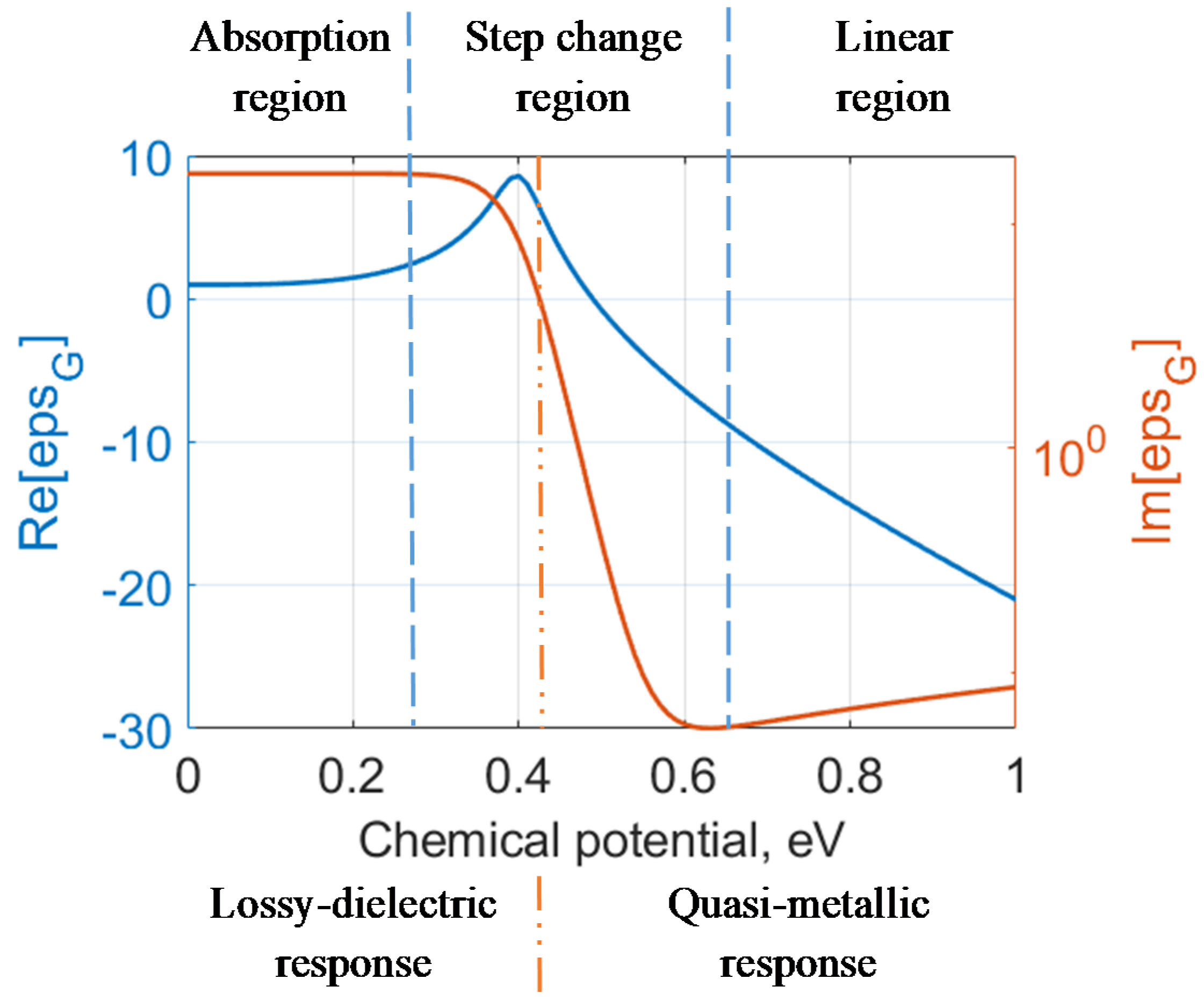
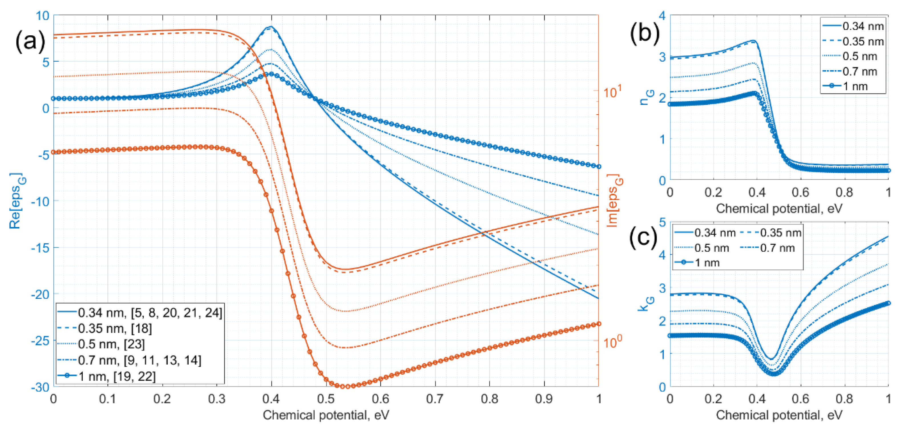
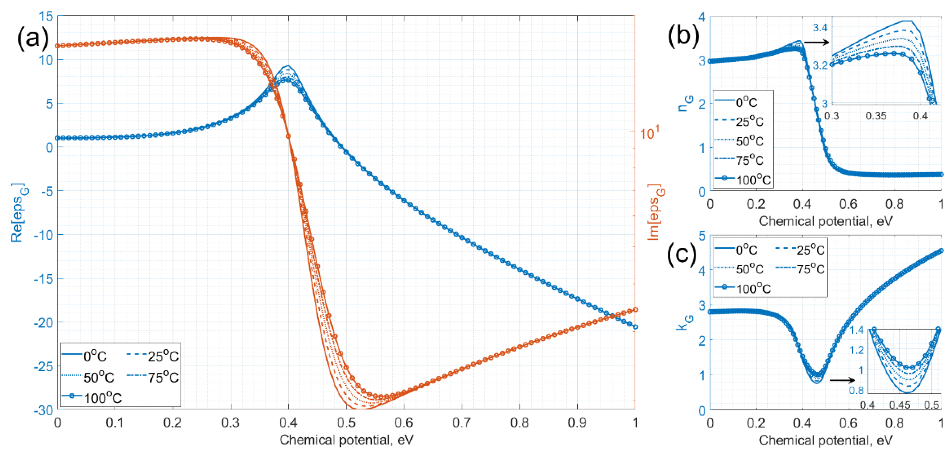
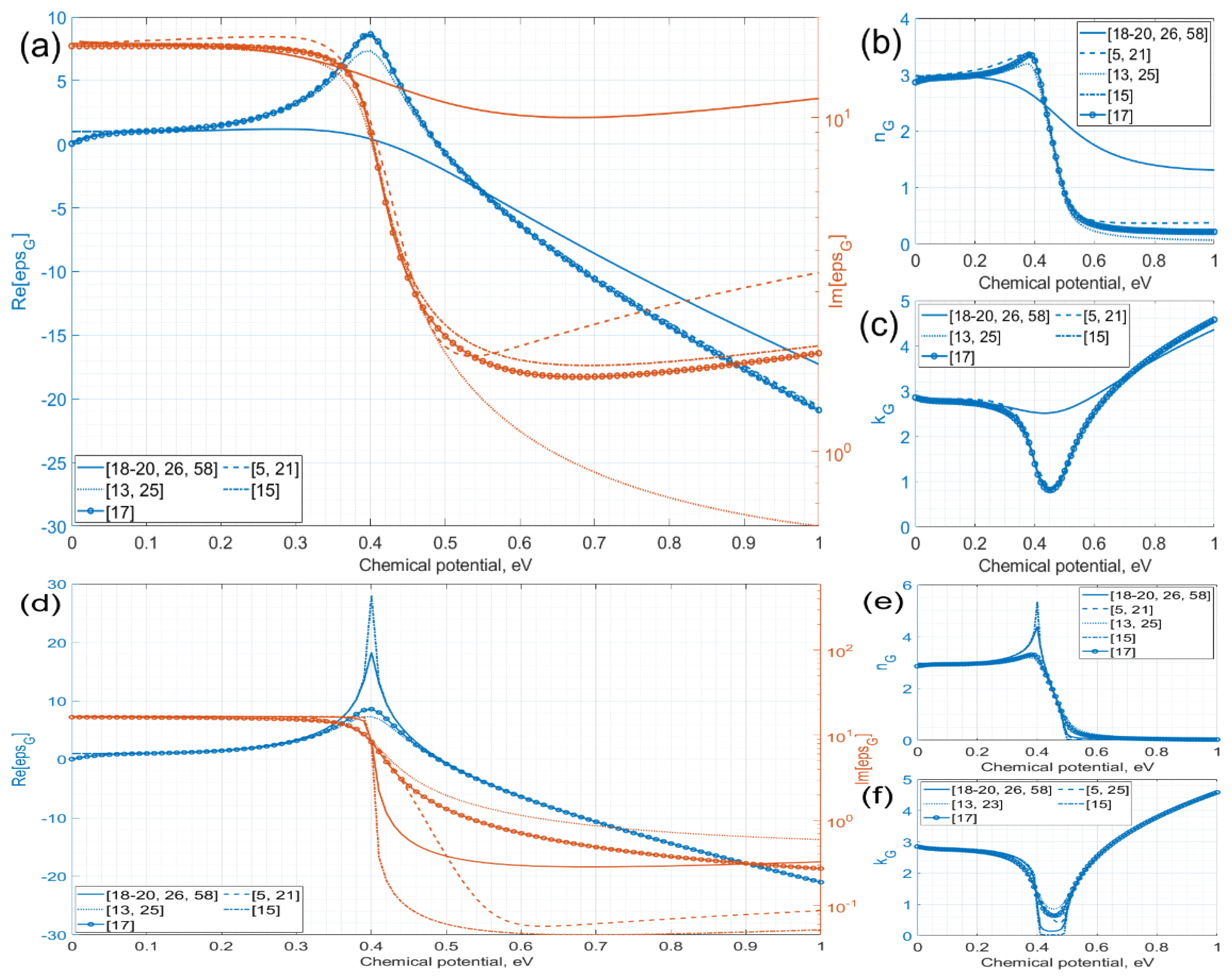
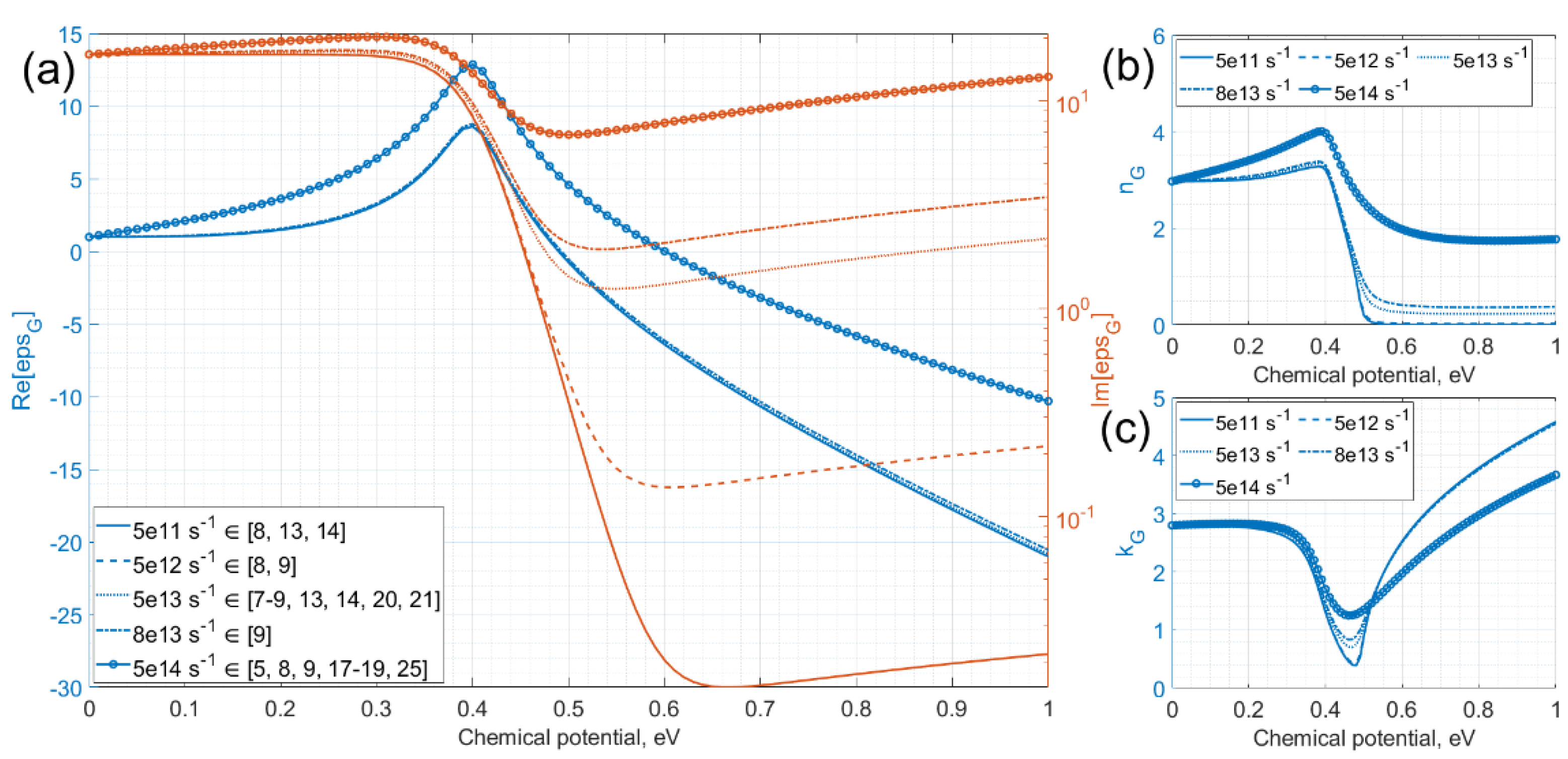
2.1.1. Dependence of Graphene Complex Permittivity

The analysis of the influence of the parameters on the complex permittivity was carried out on the basis of equation [5] at λ = 1.55 µm. Figure 1 shows the real (Re) and the imaginary (Im) parts of the graphene complex permittivity when tG = 0.34 nm, μc = 0 ÷ 1 eV, Γ = 2e12 s−1 and T = 300 K.
(a) Chemical potential
Inspection of the plot in Figure 1 (using data for both the real and imaginary parts) allows us to divide the graph into three zones: c| < 0.2 eV—dependence tending to linear, 0.2 eV < c| < 0.5 eV—transient process and c| > 0.5 eV—dependence tending to linear (for the imaginary part, the boundaries of the zones are shifted at about ~0.3 eV and ~0.6 eV, respectively). This division is close to that presented in Reference [9]. The range c| < 0.28 eV corresponds to the absorption region in which the absorption of the graphene remains high, and both the effective index and the absorption coefficient (αG = (4πf kG)/c, which have a direct proportion with extinction coefficient kG) slightly deviate, ranging from 0.0005 to 1 dB/nm, respectively. Next, the step change region (<0.64 eV) is suitable for amplitude modulation since there is a significant ‘stepping up’ of the absorption index. The final region (>0.64 eV) corresponds to low absorption, and the effective index is linear (which is applicable for phase modulation).
However, from another point of view, the zero crossing ε G _ i m (c| ≈ 0.4 eV or c| = 0.515 eV [14]) is a transition from a lossy-dielectric response (amplitude modulator mode, with the central wavelength around 1552.5–1552.8 nm [9]) to a quasi-metallic one (transition to a phase-dependent mode [9]). The imaginary part of the dielectric constant decreases significantly for Fermi levels c| > 0.4 eV, i.e., the absorption is significantly reduced. When a photon impinges on graphene, its energy may be absorbed to provoke an interband transition of a free carrier. Whether an electron or a hole is involved in this process depends on the sign of the Fermi level. According to the Pauli blocking principle, this transition can only occur if |μc| < ħω/2, at λ = 1.55 μm, c| < 0.4 eV. For an ideal, impurity-free graphene sheet (τ→∞) at zero temperature, this would reflect in an abrupt variation of absorption. At room temperature, a more gradual transmission from absorption to transparency can be expected [21]. It was found in Reference [9] that a large extinction ratio can be achieved in the operating region when c| < 0.4 eV. In the real case, switching between modes occurs smoothly, which is associated with graphene defects created during the manufacturing process [11].
(b) Graphene electrode thickness
One of the variable elements included in the Kubo model is graphene thickness. Physically, the thickness tG of the monolayer graphene is equal to about 0.34 nm while the thickness of multilayer graphene is equal to N times. Figure 2a shows the dependence of the permittivity on the chemical potential for the GE thicknesses from the considered works [5,8,9,11,13,14,18,19,20,21,24,25,26]. For example, values equal to 0.5 nm or 1 nm are used in numerical simulations to relax the mesh/grid (e.g., about 1 nm could correspond to a 3-layer graphene).
Figure 2a,b show the proportional dependence of the imaginary part of the dielectric constant on the change in the graphene thickness and refractive index (at about ~0.4 eV), respectively.
(c) Relaxation rate/scattering time
Another parameter of the Kubo model and graphene conductivity is the relaxation rate or scattering time ( Γ = τ 1 = ( e v F 2 ) / ( μ μ c ) [26], μ–charge carrier mobilities and vF–Fermi velocity (=106 m/s)), which significantly affects the imaginary part of the dielectric constant (as seen in Figure 3). It is also worth noting that the ℏΓ is the relaxation energy that defines the quality of graphene (a shorter relaxation time corresponding to a lower quality of graphene, and τ→∞ corresponds to an ideally defect-free graphene sheet) [5,14,21]. It should be noted that the Kubo model from [13] distinguishes between the relaxation rates associated with interband and intraband transitions.
Figure 3a shows that the imaginary part of the dielectric constant decreases significantly for the Fermi levels c| < 0.4 eV from the change in the scattering rate. In this case, a strong dependence of absorption on Γ is observed, since in-band absorption becomes the dominant process here. In this regime, lower values for Γ, corresponding to high carrier mobility, give lower absorption [8]. The transient process has already been described in the section on the chemical potential, but, in addition to it, it is worth noting that the final values of the relaxation time have a significant effect since there is significant absorption due to intraband scattering interactions [21]. Imperfections in the graphene layer induce density inhomogeneities, varying the optical conductivity across the graphene sheet [61].
The typical value of the Γ in fabricated graphene-based devices operating in the NIR range, varies from 5e12 s−1 to 1e14 s−1, with a minimum value of 4e9 s−1 [18]. On the experimental side, a typical value is Γ = 8e13 s−1 [9].
Figure 3b,c show the refractive index and the extinction coefficient following Equation (4).
(d) Temperature
One of the constituent parameters of the Kubo model and graphene conductivity is the temperature (in some publications the temperature is taken as the room temperature ~300 K). However, an increase in the temperature causes a slight decrease in the real and an increase in the imaginary parts of the permittivity at a chemical potential from 0.3 to 0.6 eV, which is confirmed by the curves in Figure 4.
It should be borne in mind that the levels are usually filled in accordance with the Fermi–Dirac distribution function. At zero temperature, it is a step function, from which it can be concluded that, in this case, the energy levels (which are below the chemical potential) are completely filled. The situation changes at room temperature: the distribution function expands by kBT ≈ 25 meV. The previous explanation also makes it clear that in the equilibrium state, photons at a wavelength of 1.55 μm will not be absorbed if the chemical potentials of the upper and lower graphene electrodes are equal to 0.425 eV. Therefore, when there is no applied voltage ( V G = 0), the graphene layers behave as transparent thin sheets [15].
The thermal–optical effect is not large enough to provide an equivalent change in the refractive index. Thus, the heat generated in graphene is usually transferred to the carrier waveguide or substrate. This leads to an increase in temperature and a change in the refractive index of the entire structure [62].
The work reported in Reference [18] describes a minor temperature dependence of the performance characteristics that remain practically unchanged for temperatures up to 49 °C. It should also be noted that ring or disk modulators (in contrast to the Mach–Zehnder modulator [9,18] or planar photonic crystal nanocavity-based modulator [20]) are sensitive to temperature fluctuations [63]. In References [14,64], reliable athermal operation of the modulator without a noticeable change in the speed characteristics of the device at high temperatures up to 145 °C is presented, which does not close the question of the effect of temperature on the wavelength tuning. This point is related to the effect of heat transfer—graphene electrodes are connected to the dielectric materials, which includes other dielectric materials such as Si3N4 or Si. The parameters of these materials have a higher thermal sensitivity, which can affect the stability of the tuning mechanism.

2.1.2. Graphene Conductivity Formula

The analysis of the Kubo equations was carried out following References [5,13,15,17,18,19,20,21,25] (based on its greater prevalence in the considered works). The calculated curves of the complex permittivity obtained from the combination of Kubo Formulas (1) and (2) are shown in Figure 5.
Two situations were analyzed at Γ = 8e13 s−1 and Γ = 2e12 s−1 (since this parameter depends on the quality of graphene (Section 2.1.1 (c)) and it was interesting to look at the behavior of the permittivity curves when it changes). In this regard, the changes in the Kubo model curve when this parameter changes are one of the most important criteria when choosing a formula option. In this regard, it can be noted that the [13,25] and [17] options do not react to changes in the relaxation rate. The opposite case reflects the permittivity curve obtained by the formula from [15], demonstrating the highest sensitivity. The model from [18,19,20,26,58] is “smoothed” at Γ = 8e13 s−1 (experimentally obtained result [9]), which makes it difficult to analyze the transient process. As can be seen from Figure 5a,d, the curves for the cases [5,21] show the stability of the real part of the dielectric constant to a change in the relaxation rate on the one hand, but the high sensitivity of the imaginary part on the other hand, which may be more effective, in comparison with other formulas according to the Kubo model, for modeling and analyzing graphene.

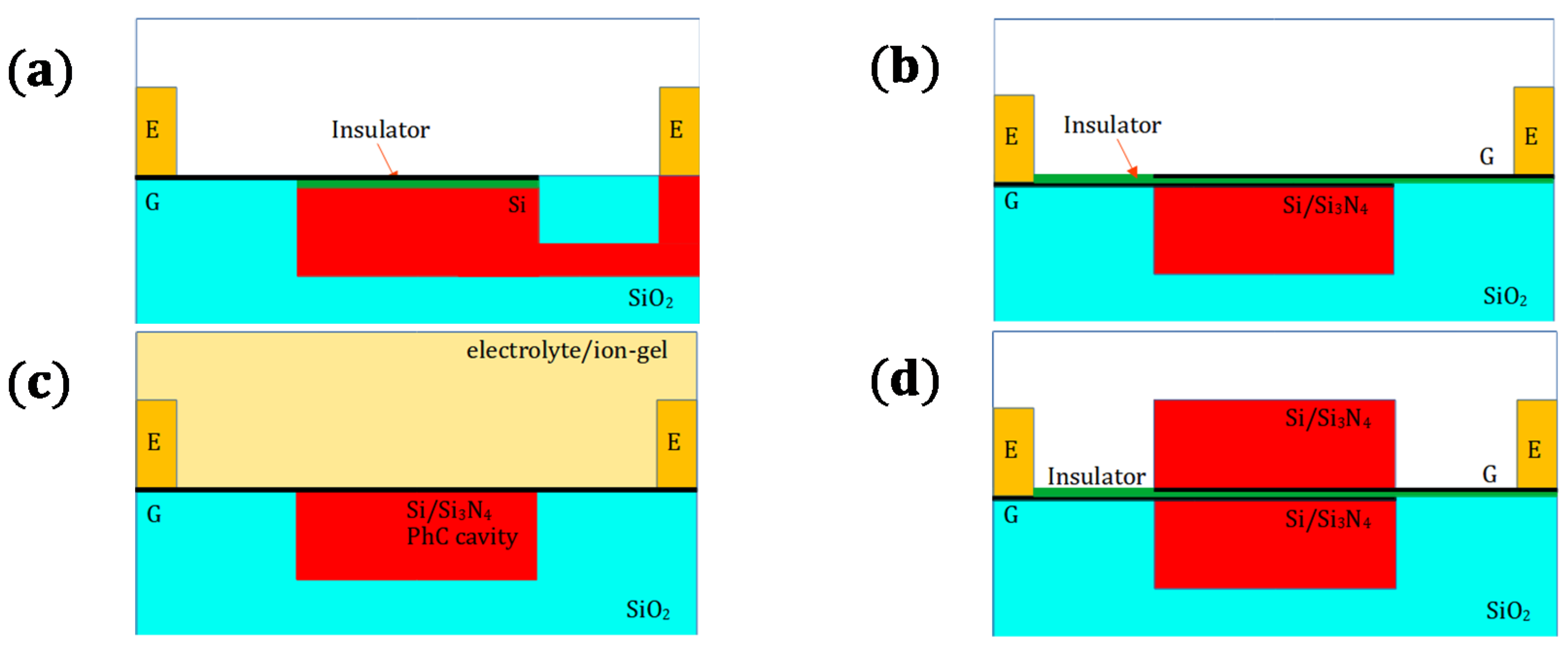
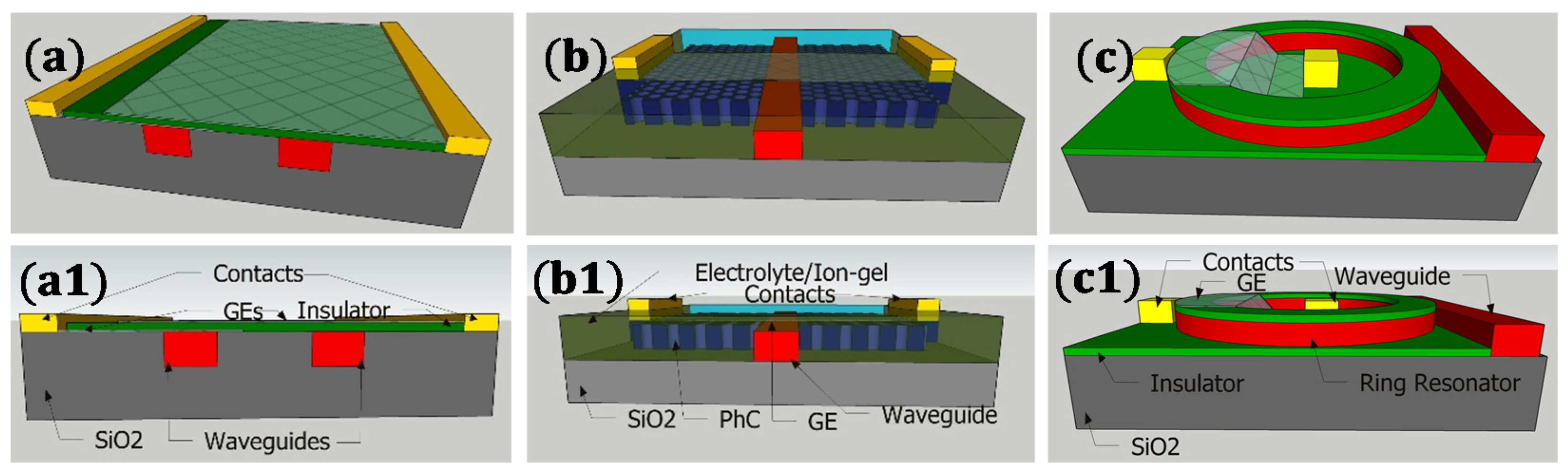
2.2. Graphene Electrode Configurations

This paragraph focuses on the analysis of graphene electrode configurations considering the relationship between the applied voltage ( V G ) and the distance between graphene electrodes ( D G ). Figure 6 shows the cross sections of the GE configurations inside the optical devices.
In particular, GE locations inside the optical devices can be categorized into two types:
(1) Graphene-Insulator-Waveguide (GIW), Figure 6a, is a single GE above the Si waveguide [5,7,9,11,13,14,17,18,19,20,21,24,25].
(1a) Electrolyte/ion-gel-Graphene-Waveguide+PhC Cavity (EGWC), Figure 6c, is the PhC Nanocavity structure, which is located under the graphene electrode [65] and, in some cases, the capacitor insulator is located on top (electrolyte or ion-gel) [7,19,20] (partly a subgroup of GIW).
(2) Graphene-Insulator-Graphene (GIG), Figure 6b, this is the case when two GEs are above the waveguide [8,10,12,15,16,21,64];
(2a) Graphene-Electrode-inside (GEin), Figure 6d, is the case when two GEs are located inside the waveguide [26,66] (partly a subgroup of GIG).
We will use the abbreviation GIW/EGWC to describe the dielectric waveguide (e.g., Si or Si3N4) that is indicated by W. The EGWC case also implies a non-use of PhC cavities (Electrolyte/ion-gel-Graphene-Waveguide).
In some configurations, e.g., EGWC, the insulator layer of the capacitor is located on the top in the form of an ion-gel or an electrolyte. In other cases, it is necessary to consider the thickness of the layers of the graphene-based capacitor. For example, a dielectric with a thickness of 90 nm [8] or 120 nm [65] between two layers of graphene causes a weak electrostatic bond, which is expressed in high applied voltages (from −40 V to 40 V). In this regard, the boundary value of D G may be 90 nm, but the optimal value will be in the range <20 nm.
However, for all configurations, the optical properties of the graphene are modulated by applying a voltage across the capacitor. For all cases, the large distance between the GE (or bottom GE) and the waveguide, which we denote as the insulator thickness (tI), leads to a relatively weak light interaction.
The Fermi level of graphene can be modulated by applying a voltage across the capacitor. In fact, the external voltage causes the accumulation of charges at the armatures of the capacitor, thus changing the carrier density on graphene and, consequently, the Fermi level as [21]
μ c ( n s ) = s g n ( n s ) ħ v F π | n s |
where ns is the graphene surface carrier density. The voltage needed to charge a GIW capacitor is a sum of two contributions: the first is the actual potential across the insulator; the second is due to the shift of the Fermi potential induced by the accumulated carriers on the graphene layer. Using Equation (6), it is possible to obtain
| V G V D i r a c | = q n s C o x + | μ c | q = q s C o x μ 2 π ( ħ v F ) 2 + | μ c | q
where C o x = ε ε 0 ( W m l / t I ) is the oxide (insulator) capacitance per unit area (∼20 mF/m2 for ion-gel [19], ∼0.493 mF/m2 for SiO2 [15], ~27 mF/m2 for polyethilenoxide (PEO) + LiClO4 [7]), and V D i r a c is the flat-band voltage corresponding to the charge-neutral Dirac point. V D i r a c depends on the intrinsic surface carrier density on the graphene electrode due to band alignment, lattice imperfections, charged defects or other impurities in the fabricated graphene sheet. In the case of a GIG capacitor, Equation (7) should be modified to account for the shift of the Fermi potential in each of the two graphene layers. In this case, the last term of Equation (7) should be modified to read as 2 | μ | / q [21].
Initially, the Fermi levels are close to the Dirac point and both graphene sheets absorb light when both graphene electrodes are undoped or lightly doped due to the interaction with the environment. When voltage is increased between the GEs, they form a simple capacitor model in which one plate is a graphene layer doped by holes and the other is a graphene layer doped by electrons at the same doping levels. When the shift of the Fermi level in both GE reaches half the photon energy of the incident light (EF = ±ħω/2), both GE become transparent at the same time. The change in the sign of the excitation voltage only switches the roles of the capacitor plates as anode and cathode and gives a similar response to incident light [12].
The limits of the applied voltage are determined by the Fermi level. The left border is determined by the moment when the Fermi level decreases (below the threshold value EF = ±ħω/2), which occurs due to the accumulation of a positive charge. This leads to the absence of electrons, which are available for interband transitions, and graphene is “transparent”. The right boundary is due to the filling of electronic states at which interband transitions are not allowed [11,24].

3. Graphene-Based Optical Devices and Tuning

In this section, we discuss the graphene-based optical device configurations in order to understand the possible options that can be exploited for wavelength tuning.
As mentioned above, several types of device configurations can be distinguished; among them, the modulators can be classified in: Mach–Zehnder graphene modulator (M-ZM) [8,9,18,67], planar photonic crystal nanocavity-based modulator (CNM) [7,10,19,20] (which represent a graphene FET transistor) and micro-ring resonator (MRR) [24,25,26,68]. Figure 7 shows some examples of these configurations.
Mach–Zehnder interferometer (MZI)-based modulators suffer from a large footprint, typically a few millimeters, while ring or disk modulators exhibit a narrow optical bandwidth, making them difficult to control and sensitive to temperature variations or fabrication errors [14]. The use of a CNM with an air gap with highly restricted modes in the central air gap improves the overlap between graphene and resonant cavity modes.
These devices can be characterized as a waveguide combined with a capacitor structure (GIW or GIG configurations) and contacts connected to GEs for voltage supply.
It should be borne in mind that there are important differences among different configurations. Assuming quasi-TM polarization, GIG-Si devices exhibit almost double the absorption with respect to that of GIW-Si devices. For TE polarization, the absorption in Si-based devices is significantly lower (up to 0.12 and 0.08 dB/μm for GIG-Si and GIW-Si devices, respectively) [14]. This is due to the interaction with the strong longitudinal component of the electric field at the upper boundary of the silicon waveguides (note that the graphene sheet does not interact with the field components outside the plane [57]). In Si3N4 devices, quasi-TE-polarized modes exhibit stronger interactions with the graphene film than quasi-TM modes. The GIG-Si3N4 has lower absorption than the GIW-Si device, but by embedding the capacitor in the Si3N4 waveguide, the absorption level of the GIG-Si3N4-Emb can be increased again, almost to that of the GIG-Si, although the waveguide is large [66].
The modulators discussed were fabricated using standard semiconductor manufacturing processes. This work uses photolithography [7,8,9,10,25] or electron beam lithography in combination with dry etching [9,11,12,13].
While silicon photonics is very promising for optical routing, a complete optical network also requires generation, modulation and light detection—which is difficult to achieve on a completely monolithic platform. Growing materials is a technologically challenging task on a silicon substrate due to the mismatch of the lattice constants and thermal expansion coefficients. Defects arising from imperfections during crystal growth also tend to limit the optical and electrical performance of such devices. One solution to this problem is to grow materials on a compatible substrate and then transfer them onto silicon [69]. In this way, it is not necessary to match lattice constants or thermal expansion coefficients as required in direct growth processes. Two-dimensional (2D) materials are a class of crystals that naturally lend themselves to this type of transfer process. Because these materials are covalently bonded in-plane and held together out-of-plane by Van der Waals forces, individual atomic planes can be mechanically separated from the bulk crystal and placed onto arbitrary substrates [70].
Since the discovery of the first isolated graphene layer prepared by mechanical exfoliation of graphite crystals, many chemical approaches to synthesize large-scale graphene have been developed, including epitaxial growth on silicon carbide and ruthenium, as well as two-dimensional assembly of reduced graphene oxides and exfoliated graphene sheets [71]. Several transfer processes are known that can be classified as “wet” or “dry” [69]. The first includes all procedures where graphene is in contact, at some stage, with a liquid. In the second, one face of graphene is protected from contacting any liquid, while the other is typically in contact with a polymer, eventually dissolved by solvents. A big problem is the development of dry transfer technology to preserve the ultra-high quality of graphene up to 450 mm in size [69]. Since graphene is a monolayer and, therefore, each of its atoms is a surface, graphene is highly sensitive to impurities left during production, transfer or manufacturing. In order to remove them, several methods have been developed (thermal annealing in H2/Ar is normally used to remove polymer residuals for cleaning after transfer and removal of solvents/surfactants in LPE graphene) [70]. Additionally, one of the problems remains the cracking of single layer graphene at the edges of the steps of the waveguide [8].
Another question that can be faced during development is the choice of material that can be used as an insulator in a capacitor implementation. One of the popular oxides in this matter is Al2O3 [8,9,10,11,12,13,18,19,24,25,64], however, in addition to it, it is advisable to use Si3N4 [21,24,26] and HfO2 [20], as well as an electrolyte in the form of a mixture of LiClO4 and polyethylene oxide (PEO) [72] or ion-gels [7,19,20]. In the Fermi levels |μc| > 0.5 eV, the optimal choice of the insulating capacitor layer formed either by one GE or two GEs, is another issue since there is the problem of graphene absorption due to interband transitions.
In this regard, Equation (6) reflects the shift of the Fermi level to |μc| = 0.5 eV, which corresponds to the electric field on the capacitor insulator
E 0.5 eV = q n s ε o x ε 0 3.6 · 10 7 ε o x [ V cm ] ,
where ε o x is the relative dielectric constant of the insulator [21]. Using Equation (8), it is possible to characterize the choice of an insulator from the point of view of performance in case of dielectric breakdown.
The analysis carried out in [21] shows that silicon nitride (Si3N4, ε o x = 7.5) is the best option among Al2O3 and SiO2 at E 0.5 eV = 5e6 V/cm at a breakdown field of about 1e7 V/cm.

Wavelength Tuning

In the previous sections, several parameters such as the scattering rate (Γ), the graphene electrode thickness (tG), the distance between graphene electrodes (DG) for the GIG structure, or the insulator thickness (tI) for others, and the applied voltage (VG) were analysed. Table 2 compares the analysed devices (all the devices are fabricated except for Reference [15]) showing that the wavelength shift ∆λ (last column) can vary from tens to thousands of picometers (last column in the table).
Wavelength shift can also be related to the variation of the refractive index using Equation (5).
The greatest influence on the tuning of the operating wavelength is exerted by a modulator based on planar photonic crystals, based on a nanocavity in combination with an electrolyte or ion-gel [7,19,20]. It should be borne in mind that in these structures, with an increase in the applied voltage, small changes in the transmission spectra can be observed until the breakdown of the device is achieved. The behavior of the device beyond this point is associated with the destruction of graphene, while the effect of plasma dispersion is still continuing. However, no further spectral shift is observed anymore, which confirms that the phase shift is mainly due to the electro-refractive effect of graphene. Although the plasma dispersion effect of doped silicon still exists, given that the doped region is relatively small and the plasma dispersion effect is weak in nature, the contribution of doped silicon is negligible [9].
Conversely, the structures of the Mach–Zehnder graphene modulator and the micro-ring resonator allow the achievement of a wavelength tuning in the range of 100–200 pm. In Reference [9], when simulating the chemical potential in the range <0.4 eV, a redshift of about 173 pm is observed. By adjusting the arm voltage, the modulation mode can be switched to a phase-dependent mode, when the chemical potential is in the range from >0.5 eV, leading to a blueshift of 385 pm (it can be achieved in this range with practically no amplitude fluctuations). The experiment showed a deterioration of these values down to 66 pm and 185 pm, respectively (due to the quality of graphene). The use of a planar photonic crystal modulator based on a nanocavity extends the tuning range up to 1–2 nm [19,20].

4. Conclusions and Future Work

This work analysed and compared the optical behaviour in the NIR range of the graphene and its integration as an electrode into optical devices. In particular, the complex permittivity, along with the parameters of the Kubo model, was discussed. The tuning mechanisms, along with the configurations for the GE the insulator material and its thickness, were detailed.
It is important to highlight that, during the fabrication, great attention should be paid to the process of transferring graphene into the waveguide since the transfer could lead to a deterioration in the quality of graphene, which greatly affects the ability of the device to tune the wavelength as it changes the surface conductivity. Particular attention should also be paid to the range of the supplied voltage since exceeding it leads to a breakdown of the tuning mechanism. Although the temperature of graphene does not lead to significant changes in the parameters of graphene, one should also consider its interaction with thermosensitive components (e.g., silicon waveguides). Finally, the performance of the analysed configurations was compared showing the achieved wavelength shift in the order of hundreds up to thousands of picometers.
In conclusion, this work could help and lead the design of the tuning of graphene-based optical devices and the integration of graphene in optical resonant structures operating in the NIR.

Author Contributions

A.S.V. performed the numerical simulations and drafted the paper. A.S.V., G.V.B., G.B., A.D., L.O., M.G. the authors commented, edited and reviewed the manuscript. M.G. supervised the work. All authors have read and agreed to the published version of the manuscript.

Funding

This research was funded by the European Union’s Horizon 2020 research and innovation programme under the Marie Skłodowska-Curie, agreement No 860808 (OPTAPHI).

Data Availability Statement

Not available.

Acknowledgments

This work has received funding from the European Union’s Horizon 2020 research and innovation programme under the Marie Skłodowska-Curie grant agreement No 860808 (OPTAPHI).

Conflicts of Interest

The authors declare no conflict of interest.

References

  1. Castro Neto, A.H.; Guinea, F.; Peres, N.M.R.; Novoselov, K.S.; Geim, A.K. The electronic properties of graphene. Rev. Mod. Phys. 2009, 81, 109–162. [Google Scholar] [CrossRef] [Green Version]
  2. Novoselov, K.S.; Geim, A.K.; Morozov, S.V.; Jiang, D.; Katsnelson, M.I.; Grigorieva, I.V.; Dubonos, S.V.; Firsov, A.A. Two-dimensional gas of massless Dirac fermions in graphene. Nature 2005, 438, 197–200. [Google Scholar] [CrossRef] [PubMed]
  3. Rinaldi, G. Nanoscience and Technology: A Collection of Reviews from Nature Journals. Assem. Autom. 2010, 30, 2. [Google Scholar] [CrossRef]
  4. Wolf, E.L. Applications of Graphene; SpringerBriefs in Materials; Springer International Publishing: Cham, Switzerland, 2014; ISBN 978-3-319-03945-9. [Google Scholar]
  5. de Ceglia, D.; Vincenti, M.A.; Grande, M.; Bianco, G.V.; Bruno, G.; D’Orazio, A.; Scalora, M. Tuning infrared guided-mode resonances with graphene. J. Opt. Soc. Am. B 2016, 33, 426. [Google Scholar] [CrossRef]
  6. Wang, F.; Zhang, Y.; Tian, C.; Girit, C.; Zettl, A.; Crommie, M.; Shen, Y.R. Gate-Variable Optical Transitions in Graphene. Science 2008, 320, 206. [Google Scholar] [CrossRef]
  7. Abdollahi Shiramin, L.; Xie, W.; Snyder, B.; De Heyn, P.; Verheyen, P.; Roelkens, G.; Van Thourhout, D. High Extinction Ratio Hybrid Graphene-Silicon Photonic Crystal Switch. IEEE Photonics Technol. Lett. 2018, 30, 157–160. [Google Scholar] [CrossRef]
  8. Mohsin, M.; Neumaier, D.; Schall, D.; Otto, M.; Matheisen, C.; Lena Giesecke, A.; Sagade, A.A.; Kurz, H. Experimental verification of electro-refractive phase modulation in graphene. Sci. Rep. 2015, 5, 10967. [Google Scholar] [CrossRef] [PubMed] [Green Version]
  9. Shu, H.; Su, Z.; Huang, L.; Wu, Z.; Wang, X.; Zhang, Z.; Zhou, Z. Significantly High Modulation Efficiency of Compact Graphene Modulator Based on Silicon Waveguide. Sci. Rep. 2018, 8, 991. [Google Scholar] [CrossRef]
  10. Cheng, Z.; Zhu, X.; Galili, M.; Frandsen, L.H.; Hu, H.; Xiao, S.; Dong, J.; Ding, Y.; Oxenløwe, L.K.; Zhang, X. Double-layer graphene on photonic crystal waveguide electro-absorption modulator with 12 GHz bandwidth. Nanophotonics 2019, 9, 2377–2385. [Google Scholar] [CrossRef]
  11. Liu, M.; Yin, X.; Ulin-Avila, E.; Geng, B.; Zentgraf, T.; Ju, L.; Wang, F.; Zhang, X. A graphene-based broadband optical modulator. Nature 2011, 474, 64–67. [Google Scholar] [CrossRef]
  12. Liu, M.; Yin, X.; Zhang, X. Double-Layer Graphene Optical Modulator. Nano Lett. 2012, 12, 1482–1485. [Google Scholar] [CrossRef] [PubMed]
  13. Phatak, A.; Cheng, Z.; Qin, C.; Goda, K. Design of electro-optic modulators based on graphene-on-silicon slot waveguides. Opt. Lett. 2016, 41, 2501. [Google Scholar] [CrossRef]
  14. Hu, Y.; Pantouvaki, M.; Van Campenhout, J.; Brems, S.; Asselberghs, I.; Huyghebaert, C.; Absil, P.; Van Thourhout, D. Broadband 10 Gb/s operation of graphene electro-absorption modulator on silicon: Broadband 10 Gb/s operation of graphene electro-absorption modulator on silicon. Laser Photonics Rev. 2016, 10, 307–316. [Google Scholar] [CrossRef] [Green Version]
  15. Bahadori-Haghighi, S.; Ghayour, R.; Sheikhi, M.H. Double-layer graphene optical modulators based on Fano resonance in all-dielectric metasurfaces. J. Appl. Phys. 2019, 125, 073104. [Google Scholar] [CrossRef]
  16. Koester, S.J.; Li, M. High-speed waveguide-coupled graphene-on-graphene optical modulators. Appl. Phys. Lett. 2012, 100, 171107. [Google Scholar] [CrossRef]
  17. Luo, X.; Zhai, X.; Li, H.; Liu, J.; Wang, L. Tunable Nonreciprocal Graphene Waveguide With Kerr Nonlinear Material. IEEE Photonics Technol. Lett. 2017, 29, 1903–1906. [Google Scholar] [CrossRef]
  18. Xu, C.; Jin, Y.; Yang, L.; Yang, J.; Jiang, X. Characteristics of electro-refractive modulating based on Graphene-Oxide-Silicon waveguide. Opt. Express 2012, 20, 22398. [Google Scholar] [CrossRef] [PubMed] [Green Version]
  19. Majumdar, A.; Kim, J.; Vuckovic, J.; Wang, F. Electrical Control of Silicon Photonic Crystal Cavity by Graphene. Nano Lett. 2013, 13, 515–518. [Google Scholar] [CrossRef] [PubMed] [Green Version]
  20. Gan, X.; Shiue, R.-J.; Gao, Y.; Mak, K.F.; Yao, X.; Li, L.; Szep, A.; Walker, D.; Hone, J.; Heinz, T.F.; et al. High-Contrast Electrooptic Modulation of a Photonic Crystal Nanocavity by Electrical Gating of Graphene. Nano Lett. 2013, 13, 691–696. [Google Scholar] [CrossRef] [PubMed] [Green Version]
  21. Sorianello, V.; Midrio, M.; Romagnoli, M. Design optimization of single and double layer Graphene phase modulators in SOI. Opt. Express 2015, 23, 6478. [Google Scholar] [CrossRef]
  22. Phare, C.T.; Lee, Y.-H.D.; Cardenas, J.; Lipson, M. 30 GHz Zeno-based Graphene Electro-optic Modulator. In Proceedings of the CLEO: 2015, San Jose, CA, USA, 5–10 May 2015; OSA: San Jose, CA, USA, 2015; p. SW4I.4. [Google Scholar]
  23. Cai, M.; Wang, S.; Liu, Z.; Wang, Y.; Han, T.; Liu, H. Graphene Electro-Optical Switch Modulator by Adjusting Propagation Length Based on Hybrid Plasmonic Waveguide in Infrared Band. Sensors 2020, 20, 2864. [Google Scholar] [CrossRef]
  24. Ding, Y.; Zhu, X.; Xiao, S.; Hu, H.; Frandsen, L.H.; Mortensen, N.A.; Yvind, K. Effective Electro-Optical Modulation with High Extinction Ratio by a Graphene–Silicon Microring Resonator. Nano Lett. 2015, 15, 4393–4400. [Google Scholar] [CrossRef] [Green Version]
  25. Qiu, C.; Gao, W.; Vajtai, R.; Ajayan, P.M.; Kono, J.; Xu, Q. Efficient Modulation of 1.55 μm Radiation with Gated Graphene on a Silicon Microring Resonator. Nano Lett. 2014, 14, 6811–6815. [Google Scholar] [CrossRef] [PubMed] [Green Version]
  26. Yang, L.; Hu, T.; Shen, A.; Pei, C.; Li, Y.; Dai, T.; Yu, H.; Li, Y.; Jiang, X.; Yang, J. Proposal for a 2X2 Optical Switch Based on Graphene-Silicon-Waveguide Microring. IEEE Photonics Technol. Lett. 2014, 26, 235–238. [Google Scholar] [CrossRef]
  27. Grande, M.; Bianco, G.V.; Laneve, D.; Capezzuto, P.; Petruzzelli, V.; Scalora, M.; Prudenzano, F.; Bruno, G.; D’Orazio, A. Gain and phase control in a graphene-loaded reconfigurable antenna. Appl. Phys. Lett. 2019, 115, 133103. [Google Scholar] [CrossRef]
  28. Grande, M.; Bianco, G.V.; Perna, F.M.; Capriati, V.; Capezzuto, P.; Scalora, M.; Bruno, G.; D’Orazio, A. Reconfigurable and optically transparent microwave absorbers based on deep eutectic solvent-gated graphene. Sci. Rep. 2019, 9, 5463. [Google Scholar] [CrossRef]
  29. Grande, M.; Bianco, G.V.; Capezzuto, P.; Petruzzelli, V.; Prudenzano, F.; Scalora, M.; Bruno, G.; D’Orazio, A. Amplitude and phase modulation in microwave ring resonators by doped CVD graphene. Nanotechnology 2018, 29, 325201. [Google Scholar] [CrossRef] [PubMed]
  30. Sensale-Rodriguez, B.; Yan, R.; Kelly, M.M.; Fang, T.; Tahy, K.; Hwang, W.S.; Jena, D.; Liu, L.; Xing, H.G. Broadband graphene terahertz modulators enabled by intraband transitions. Nat. Commun. 2012, 3, 780. [Google Scholar] [CrossRef]
  31. Sensale-Rodriguez, B.; Yan, R.; Rafique, S.; Zhu, M.; Li, W.; Liang, X.; Gundlach, D.; Protasenko, V.; Kelly, M.M.; Jena, D.; et al. Extraordinary Control of Terahertz Beam Reflectance in Graphene Electro-absorption Modulators. Nano Lett. 2012, 12, 4518–4522. [Google Scholar] [CrossRef] [PubMed] [Green Version]
  32. Lee, C.-C.; Suzuki, S.; Xie, W.; Schibli, T.R. Broadband graphene electro-optic modulators with sub-wavelength thickness. Opt. Express 2012, 20, 5264. [Google Scholar] [CrossRef] [PubMed]
  33. Ono, M.; Hata, M.; Tsunekawa, M.; Nozaki, K.; Sumikura, H.; Chiba, H.; Notomi, M. Ultrafast and energy-efficient all-optical switching with graphene-loaded deep-subwavelength plasmonic waveguides. Nat. Photonics 2020, 14, 37–43. [Google Scholar] [CrossRef] [Green Version]
  34. Garmire, E. Nonlinear optics in daily life. Opt. Express 2013, 21, 30532. [Google Scholar] [CrossRef] [PubMed]
  35. Hafez, H.A.; Kovalev, S.; Tielrooij, K.; Bonn, M.; Gensch, M.; Turchinovich, D. Terahertz Nonlinear Optics of Graphene: From Saturable Absorption to High-Harmonics Generation. Adv. Opt. Mater. 2020, 8, 1900771. [Google Scholar] [CrossRef] [Green Version]
  36. Bowlan, P.; Martinez-Moreno, E.; Reimann, K.; Elsaesser, T.; Woerner, M. Ultrafast terahertz response of multilayer graphene in the nonperturbative regime. Phys. Rev. B 2014, 89, 041408. [Google Scholar] [CrossRef]
  37. Hafez, H.A.; Kovalev, S.; Deinert, J.-C.; Mics, Z.; Green, B.; Awari, N.; Chen, M.; Germanskiy, S.; Lehnert, U.; Teichert, J.; et al. Extremely efficient terahertz high-harmonic generation in graphene by hot Dirac fermions. Nature 2018, 561, 507–511. [Google Scholar] [CrossRef]
  38. Deinert, J.-C.; Alcaraz Iranzo, D.; Pérez, R.; Jia, X.; Hafez, H.A.; Ilyakov, I.; Awari, N.; Chen, M.; Bawatna, M.; Ponomaryov, A.N.; et al. Grating-Graphene Metamaterial as a Platform for Terahertz Nonlinear Photonics. ACS Nano 2021, 15, 1145–1154. [Google Scholar] [CrossRef]
  39. Hasan, T.; Sun, Z.; Wang, F.; Bonaccorso, F.; Tan, P.H.; Rozhin, A.G.; Ferrari, A.C. Nanotube–Polymer Composites for Ultrafast Photonics. Adv. Mater. 2009, 21, 3874–3899. [Google Scholar] [CrossRef]
  40. Sobon, G.; Sotor, J.; Pasternak, I.; Krzempek, K.; Strupinski, W.; Abramski, K.M. A tunable, linearly polarized Er-fiber laser mode-locked by graphene/PMMA composite. Laser Phys. 2013, 23, 125101. [Google Scholar] [CrossRef]
  41. Jung, M.; Koo, J.; Park, J.; Song, Y.-W.; Jhon, Y.M.; Lee, K.; Lee, S.; Lee, J.H. Mode-locked pulse generation from an all-fiberized, Tm-Ho-codoped fiber laser incorporating a graphene oxide-deposited side-polished fiber. Opt. Express 2013, 21, 20062. [Google Scholar] [CrossRef] [PubMed]
  42. Lin, Y.-H.; Yang, C.-Y.; Liou, J.-H.; Yu, C.-P.; Lin, G.-R. Using graphene nano-particle embedded in photonic crystal fiber for evanescent wave mode-locking of fiber laser. Opt. Express 2013, 21, 16763. [Google Scholar] [CrossRef]
  43. Choi, S.Y.; Jeong, H.; Hong, B.H.; Rotermund, F.; Yeom, D.-I. All-fiber dissipative soliton laser with 10.2 nJ pulse energy using an evanescent field interaction with graphene saturable absorber. Laser Phys. Lett. 2014, 11, 015101. [Google Scholar] [CrossRef]
  44. Morell, N.; Reserbat-Plantey, A.; Tsioutsios, I.; Schädler, K.G.; Dubin, F.; Koppens, F.H.L.; Bachtold, A. High Quality Factor Mechanical Resonators Based on WSe2 Monolayers. Nano Lett. 2016, 16, 5102–5108. [Google Scholar] [CrossRef] [Green Version]
  45. Chhowalla, M.; Shin, H.S.; Eda, G.; Li, L.-J.; Loh, K.P.; Zhang, H. The chemistry of two-dimensional layered transition metal dichalcogenide nanosheets. Nat. Chem. 2013, 5, 263–275. [Google Scholar] [CrossRef]
  46. Low, T.; Chaves, A.; Caldwell, J.D.; Kumar, A.; Fang, N.X.; Avouris, P.; Heinz, T.F.; Guinea, F.; Martin-Moreno, L.; Koppens, F. Polaritons in layered two-dimensional materials. Nat. Mater. 2017, 16, 182–194. [Google Scholar] [CrossRef] [Green Version]
  47. Correas-Serrano, D.; Gomez-Diaz, J.S.; Melcon, A.A.; Alù, A. Black phosphorus plasmonics: Anisotropic elliptical propagation and nonlocality-induced canalization. J. Opt. 2016, 18, 104006. [Google Scholar] [CrossRef] [Green Version]
  48. Xia, F.; Wang, H.; Jia, Y. Rediscovering black phosphorus as an anisotropic layered material for optoelectronics and electronics. Nat. Commun. 2014, 5, 4458. [Google Scholar] [CrossRef] [Green Version]
  49. Wang, H.; Yu, X. Few-Layered Black Phosphorus: From Fabrication and Customization to Biomedical Applications. Small 2018, 14, 1702830. [Google Scholar] [CrossRef] [PubMed]
  50. Huang, Y.; Qiao, J.; He, K.; Bliznakov, S.; Sutter, E.; Chen, X.; Luo, D.; Meng, F.; Su, D.; Decker, J.; et al. Interaction of Black Phosphorus with Oxygen and Water. Chem. Mater. 2016, 28, 8330–8339. [Google Scholar] [CrossRef] [Green Version]
  51. Li, L.; Yu, Y.; Ye, G.J.; Ge, Q.; Ou, X.; Wu, H.; Feng, D.; Chen, X.H.; Zhang, Y. Black phosphorus field-effect transistors. Nat. Nanotechnol. 2014, 9, 372–377. [Google Scholar] [CrossRef] [Green Version]
  52. Das, S.; Zhang, W.; Demarteau, M.; Hoffmann, A.; Dubey, M.; Roelofs, A. Tunable Transport Gap in Phosphorene. Nano Lett. 2014, 14, 5733–5739, Correction in 2016, 16, 2122–2122. [Google Scholar] [CrossRef] [PubMed]
  53. Rudenko, A.N.; Yuan, S.; Katsnelson, M.I. Toward a realistic description of multilayer black phosphorus: From G W approximation to large-scale tight-binding simulations. Phys. Rev. B 2015, 92, 085419. [Google Scholar] [CrossRef] [Green Version]
  54. Kozawa, D.; Kumar, R.; Carvalho, A.; Kumar Amara, K.; Zhao, W.; Wang, S.; Toh, M.; Ribeiro, R.M.; Castro Neto, A.H.; Matsuda, K.; et al. Photocarrier relaxation pathway in two-dimensional semiconducting transition metal dichalcogenides. Nat. Commun. 2014, 5, 4543. [Google Scholar] [CrossRef] [PubMed]
  55. Low, T.; Rodin, A.S.; Carvalho, A.; Jiang, Y.; Wang, H.; Xia, F.; Castro Neto, A.H. Tunable optical properties of multilayer black phosphorus thin films. Phys. Rev. B 2014, 90, 075434. [Google Scholar] [CrossRef] [Green Version]
  56. Depine, R.A. Electromagnetics of graphene. In Graphene Optics: Electromagnetic Solution of Canonical Problems; Morgan & Claypool Publishers: San Rafael, CA, USA, 2016; pp. 1–136. ISBN 978-1-68174-309-7. [Google Scholar]
  57. Hanson, G.W. Dyadic Green’s functions and guided surface waves for a surface conductivity model of graphene. J. Appl. Phys. 2008, 103, 064302. [Google Scholar] [CrossRef] [Green Version]
  58. Polycarpou, A.C. Introduction to the Finite Element Method in Electromagnetics; Morgan & Claypool: San Rafael, CA, USA, 2006; pp. 1–126. ISBN 978-1-59829-047-9. [Google Scholar]
  59. Introduction—MEEP Documentation. Available online: https://meep.readthedocs.io/en/latest/Introduction/ (accessed on 19 April 2021).
  60. Wartak, M.S. Computational Photonics: An Introduction with MATLAB; Cambridge University Press: Cambridge, UK, 2013; ISBN 978-1-107-00552-5. [Google Scholar]
  61. Tan, Y.-W.; Zhang, Y.; Bolotin, K.; Zhao, Y.; Adam, S.; Hwang, E.H.; Das Sarma, S.; Stormer, H.L.; Kim, P. Measurement of Scattering Rate and Minimum Conductivity in Graphene. Phys. Rev. Lett. 2007, 99, 246803. [Google Scholar] [CrossRef] [PubMed] [Green Version]
  62. Bao, Q.; Loh, K.P. Graphene Photonics, Plasmonics, and Broadband Optoelectronic Devices. ACS Nano 2012, 6, 3677–3694. [Google Scholar] [CrossRef] [PubMed]
  63. Timurdogan, E.; Sorace-Agaskar, C.M.; Sun, J.; Shah Hosseini, E.; Biberman, A.; Watts, M.R. An ultralow power athermal silicon modulator. Nat. Commun. 2014, 5, 4008. [Google Scholar] [CrossRef] [Green Version]
  64. Dalir, H.; Xia, Y.; Wang, Y.; Zhang, X. Athermal Broadband Graphene Optical Modulator with 35 GHz Speed. ACS Photonics 2016, 3, 1564–1568. [Google Scholar] [CrossRef]
  65. Chen, X.; Wang, F.; Gu, Q.; Yang, J.; Yu, M.; Kwong, D.; Wong, C.W.; Yang, H.; Zhou, H.; Zhou, S. Multifunctional optoelectronic device based on graphene-coupled silicon photonic crystal cavities. Opt. Express 2021, 29, 11094. [Google Scholar] [CrossRef]
  66. Abdollahi Shiramin, L.; Van Thourhout, D. Graphene Modulators and Switches Integrated on Silicon and Silicon Nitride Waveguide. IEEE J. Sel. Top. Quantum Electron. 2017, 23, 94–100. [Google Scholar] [CrossRef]
  67. Sorianello, V.; Midrio, M.; Contestabile, G.; Asselberghs, I.; Van Campenhout, J.; Huyghebaert, C.; Goykhman, I.; Ott, A.K.; Ferrari, A.C.; Romagnoli, M. Graphene–silicon phase modulators with gigahertz bandwidth. Nat. Photonics 2018, 12, 40–44. [Google Scholar] [CrossRef]
  68. Phare, C.T.; Daniel Lee, Y.-H.; Cardenas, J.; Lipson, M. Graphene electro-optic modulator with 30 GHz bandwidth. Nat. Photonics 2015, 9, 511–514. [Google Scholar] [CrossRef]
  69. Ferrari, A.C.; Bonaccorso, F.; Fal’ko, V.; Novoselov, K.S.; Roche, S.; Bøggild, P.; Borini, S.; Koppens, F.H.L.; Palermo, V.; Pugno, N.; et al. Science and technology roadmap for graphene, related two-dimensional crystals, and hybrid systems. Nanoscale 2015, 7, 4598–4810. [Google Scholar] [CrossRef] [PubMed] [Green Version]
  70. Youngblood, N.; Li, M. Integration of 2D materials on a silicon photonics platform for optoelectronics applications. Nanophotonics 2016, 6, 1205–1218. [Google Scholar] [CrossRef]
  71. Kim, K.S.; Zhao, Y.; Jang, H.; Lee, S.Y.; Kim, J.M.; Kim, K.S.; Ahn, J.-H.; Kim, P.; Choi, J.-Y.; Hong, B.H. Large-scale pattern growth of graphene films for stretchable transparent electrodes. Nature 2009, 457, 706–710. [Google Scholar] [CrossRef] [PubMed]
  72. Li, H.-M.; Xu, K.; Bourdon, B.; Lu, H.; Lin, Y.-C.; Robinson, J.A.; Seabaugh, A.C.; Fullerton-Shirey, S.K. Electric Double Layer Dynamics in Poly(ethylene oxide) LiClO4 on Graphene Transistors. J. Phys. Chem. C 2017, 121, 16996–17004. [Google Scholar] [CrossRef]
Figure 1. Zoning of the Kubo model in the c| range from 0 to 1 eV using the example of the results obtained from Equation (1) from Reference [5].
Applsci 11 08367 g001
Figure 2. (a) Real (blue curves) and imaginary (red curves) parts of the permittivity, (b) refractive index and (c) extinction coefficient as a function of chemical potential for different GE thicknesses from various publications ( λ = 1.55 µm, t G = 0.34 ÷ 1 nm, μ c = 0 ÷ 1 eV, Γ = 8e13 s−1, T = 300 K).
Applsci 11 08367 g002
Figure 3. (a) Real (blue curves) and imaginary (red curves) parts of the permittivity, (b) refractive index and (c) extinction coefficient as a function of the chemical potential for different values of relaxation rate from various publications ( λ = 1.55 µm, t G = 0.34 nm, μ c = 0 ÷ 1 eV, Γ = 5e11 ÷ 5e14 s−1, T = 300 K).
Applsci 11 08367 g003
Figure 4. (a) Real (blue curves) and imaginary (red curves) parts of the permittivity, (b) refractive index and (c) extinction coefficient as a function of the temperature from various publications ( λ = 1.55   µ m ,   t G = 0.34 nm, μ c = 0 ÷ 1 eV, Γ = 8e13 s−1, T = 0 ÷ 100 °C).
Applsci 11 08367 g004
Figure 5. (a) Real (blue curves) and imaginary (red curves) parts of the permittivity, (b) refractive index and (c) extinction coefficient as a function of the chemical potential from various publications, when λ = 1.55 µm, t G = 0.34 nm, μ c = 0 ÷ 1 eV, Γ = 8e13 s−1 and T = 300 K. (d) Real and imaginary parts of the permittivity, (e) refractive index and (f) extinction coefficient as a function of the chemical potential from various publications, when λ = 1.55 µm, t G = 0.34 nm, μ c = 0 ÷ 1 eV, Γ = 2e12 s−1, T = 300 K.
Applsci 11 08367 g005
Figure 6. Sketches of the location of graphene electrodes: (a) Graphene-Insulator-Waveguide (GIW), (b) Graphene-Insulator-Graphene (GIG), (c) Electrolyte/ion-gel-Graphene-Waveguide+PhC Cavity (EGWC) and (d) Graphene-Insulator-Graphene inside waveguide (GEin). (G–Graphene electrode and E–electrode).
Applsci 11 08367 g006
Figure 7. Examples of the device configurations: (a,a1) Mach–Zehnder graphene modulator (M-ZM), (b,b1) planar photonic crystal nanocavity-based modulator (CNM) and (c,c1)–micro-ring resonator (MRR).
Applsci 11 08367 g007
Table 1. The list of symbols and notations.
SymbolDescription
λ and Δλwavelength and its shift
σ ( σ G ), σ   and σ surface conductivity (graphene surface conductivity), intraband σ i n t r a and interband σ i n t e r conductivities
ε ( ε G ), ε G _ r e and ε G _ i m complex permittivity (graphene complex permittivity), its real and imaginary parts
n ( n G ) and Δnrefractive index (graphene refractive index) and its change
nsgraphene surface carrier density
k ( k G )extinction coefficient (graphene extinction coefficient)
eelectron charge
ω radian frequency
ħ = h / 2 π ħ = h / 2 π , reduced Planck constant
Γ and   τ phenomenological scattering rate and τ = 1 / Γ , relaxation time
f d ( ξ ) f d ( ξ ) = ( e ( ξ μ c ) / k B T + 1 ) 1 , Fermi-Dirac distribution ( ξ –energy)
k B Boltzmann’s constant
Ttemperature
μ c chemical potential
μcharge carrier mobilities
v F Fermi velocity
t G and t I graphene and insulator thicknesses
Lgraphene length
dspacing between minima or free spectral range
D G distance between graphene electrodes
φphase shift
V G and V D i r a c applied voltage and flat-band voltage corresponding to the charge-neutral Dirac point
C o x C o x = ε ε 0 ( W m l / t I ) , oxide (insulator) capacitance per unit area
GEGraphene Electrode
GIWGraphene-Insulator-Waveguide
GIGGraphene-Insulator-Graphene
EGWCElectrolyte/ion-gel-Graphene-Waveguide+PhC Cavity
GEinGraphene-Insulator-Graphene inside waveguide
M-ZMMach–Zehnder Graphene Modulator
CNMCrystal Nanocavity-based Modulator
MRRMicro-ring Resonator
Table 2. Comparison table (* refers to fabricated devices).
Ref.tG, nmTMMtI, nmΓ, s−1Insulator
Material
VGλ, µmDevice Type Δ λ ,   pm
[7] *-EGWC-3.8462e13PEO + LiClO4−1.2 ÷ 1.2 V1.56907CNM800
[8] *0.33GIG905e11 ÷ 1e14Al2O3−40 ÷ 40 V1.53–1.57M-ZM140
[9] *0.7GIG105e12 ÷ 1e14, 8e13 (Γexp)Al2O30 ÷ 3 V
0 ÷ 1 V/1 ÷ 3 V
1.552M-ZM173/385
[10] *-GIG5-Al2O30 ÷ 15 V1.549CNM66/165
[15]0.34GIG701e14SiO2−4.95 ÷ 4.95 V1.539–1.559WOM10
[19] *1EGWC52.2789e14Al2O3 &
ion-gel
−2 ÷ 0 V1.55CNM1000
[20] *0.34EGWC107.5963e13HfO2 &
PEO + LiClO4
−7 ÷ 6 V1.55CNM1000
[24] *1GIW--Al2O3−12.5 ÷ 0 V1.548–1.557MRR2000
[25] *0.5GIW251e14Al2O3−6 ÷ 6 V1.55MRR125
Publisher’s Note: MDPI stays neutral with regard to jurisdictional claims in published maps and institutional affiliations.

