Abstract
SEO100c, an EO-polymer, has been reported of having an r33 in excess of 100 pm/V. Experimental poling research was performed on rib waveguide modulator for device design and development. Reported is the determination of the impact that temperature and voltage have on the poling of a SEO100c waveguide device in order to maximize the r33 while avoiding damage to the device structure ensuring high yield in manufacture. The poling process is shown to have a nonlinear relationship between r33 and poling field aiding in the selection of achievable poling voltages for required r33 values. Device thermal stability is quantified and reported for the complete poling process and the impacts upon r33. Investigation into the possible relaxation of device r33 is measured over an extended period demonstrating desirable use within deployable devices.
1. Introduction
Electro-Optic (EO) waveguide modulators are essential in optical communications to convert electrical signals to optical signals. EO modulators produce cleaner modulated signals and provide faster modulation rates than direct modulation options [1]. The majority of commercial EO modulators utilize lithium niobate which has a maximum r33 tensor of 30.8 pm/V [2] limiting the reduction in Vπ (on-off voltage) for most modest laser power. To achieve devices with a low Vπ, commercial lithium niobate devices must increase the interaction length (L) of the electro-optic effect. This results a figure of merit Vπ-L being vital describe optimization of device size and Vπ. Alternative to lithium niobate are electro optic polymers, which consist of a polymer matrix, commonly polycarbonate or PMMA, and nonlinear EO chromophore molecules [3]. EO polymers with r33 values in excess of 100 pm/V have been reported [4,5] allowing low voltage designs since the tensor is inversely proportional to the modulator on-off voltage. This high r33 value also allows for low Vπ-L values to be achievable.
For EO polymers to obtain an r33, the chromophores must first be aligned through a poling process [6]. Poling involves heating the EO polymer structure to its glass transition temperature while applying a strong electric field across the EO polymer. Various methods of efficient poling to reach maximum r33 while avoiding dielectric breakdown have been demonstrated including corona poling [7], and contact poling [6]. Corona poling is not used due to the need for voltages in excess of 3 kV, and non-uniform polling of EO-Layers [7].
Utilizing the contact poling method/process involves electrodes surrounding the EO-polymer to distribute an electric field. Contact poling can be used to pole a single film of EO polymer or full device stacks. The highest r33′s reported have been for single films of EO-polymers maximizing the static field within the active layer by eliminating the clad resistive layers. Single films of the EO-polymer can be directly sandwiched between two electrodes to get a strong electric field across the polymer layer and provide efficient poling. Single EO-Polymer films can be poled and their r33 can be measured using the teng-man measurement technique [8]. However, this is not practical for waveguide devices as the electrodes would quickly attenuate any optical power. Using a full device stack of a cladding-core-cladding waveguide structure between the polling electrodes allows the waveguides to be fully fabricated and then poled. A major advantage of contact poling is that a device can be poled multiple times under various conditions and can be re-poled if the chromophore alignment relaxes. Relaxation of chromophore alignment can impact the lifespan of an EO polymer device [9,10]. The contact poling method results in the electric field being distributed between the cladding and core layers, requiring a higher applied voltage to get equivalent poling results. This higher voltage introduces additional risks to the poling process as the high voltage may cause arcing between electrodes or cause a dielectric break down in any of the device layers. A preferred method to ensure maximization of r33 for a wave-guiding device structure is to pole utilizing the mid-process poling technique [6]. Mid-process poling is performed after the core layer has been fabricated, allowing poling to be carried out on a partial stack of cladding-core layers, reducing the required applied voltage, and maximizing r33.
The electrode size is also a significant factor in the poling process. Electrode size and position for an EO-Modulator are often constrained by the RF operational design frequency. Electrodes are patterned over the modulating part of the waveguide structure to pole the necessary section of the waveguide. Having the electrode over only the waveguide reduces the risk of dielectric breakdown. EO-Modulator designs may require a larger electrode for their end application, such as in the case of an EO antenna [11]. Additionally large area poling can be used in poling full wafers before individual devices are diced. The use of a large poling electrode will result in the poling of a larger section of the core material but increases the risk of shorting through the device and rendering it unusable. Because a larger area is being poled there is higher probability of the poling E-field finding a material imperfection. Any imperfection such as a dust particle or an air bubble in the poled area can result in dielectric breakdown.
Inherent to the polling process of EO-polymers is the risk of dielectric breakdown. This risk is introduced by the combination of heating the polymer to the glass transition temperature which lowers the breakdown voltage while applying a high strength field to the device. For these reasons the effects of poling SEO100c at lower voltages and lower temperatures have been examined, minimizing of the risk of dielectric breakdown at the expense of a lower r33.
A large r33 of 226 pm/V has been reported in a TiO2/SEO100c/TiO2 multilayer structure measured using the teng-man method [8]. An r33 of 166 pm/V has been reported for a directional coupler using SEO100c with a proprietary cladding material [4]. This paper reports and quantifies the research of r33 measurements poled under increasingly stronger electric fields of the EO polymer SEO100c for application designers. Of particular interest is the achievable r33 in a practical waveguide EO modulator, constructed using commercial polymers under various poling conditions. A polymer modulator made from commercially available products demonstrates the progress that has been made in EO polymer design.
2. Device Geometry
Single mode rib waveguides were fabricated utilizing a core layer of the EO polymer SEO100c with cladding layers of NOA73. The Single mode rib waveguide geometry is shown in Figure 1. To ensure single mode operation the ratios of the height of the EO slab (h) and EO waveguide (H) need to be properly selected. A h/H ratio of 0.75 was chosen to as described by Souren et al. [12]. This single mode operation was then confirmed by calculating the effective index of the fundamental slab mode and the 1st order rib mode and verifying that the fundamental slab mode effective index was smaller. This geometry was designed around minimizing coupling loss between the input fiber (Thorlabs P1-980PM) and the waveguide. The cladding layers were made thick enough to ensure no optical mode loss from the proximity of the electrodes [13]. The radial bend design provides numerous path lengths on a single device. The waveguide length of the devices ranged from 1.74 cm to 3.63 cm. These longer path lengths allow small r33 values to be measured. Designing waveguides with a large radius of curvature (>0.5 cm) the resulting bending loss is insignificant.

Figure 1.
Completed polymer stack for the waveguide devices.
3. Waveguide Fabrication
The first step in the fabrication process was using e-beam deposition to deposit 10 nm of chrome adhesion layer followed by 100 nm of gold on a silicon wafer to form the bottom electrode. A 4.3 μm layer of Norland Products NOA 73 was spun on using a static spinning technique, then UV cured for 30 min with low intensity UV to form a smooth bottom cladding layer.
To create the core layer, a vial with 0.5 g of SEO100c had 7.45 g of dibromomethane added. The solution was then mixed on a rotator at 35 rpm for 8.5 h. Once mixed, the SEO100c was passed through a 0.2 μm nylon filter and allowed to settle for 30 min. After settling, the SEO100c was deposited by a static spinning process with a spin speed of 1000 rpm for 40 s producing a 2.7 μm-thick core layer. The wafer was then baked in a vacuum oven at 75 °C for 18 h.
A layer of Futurrex’s PR1-1000a photoresist was spun on, photolithography was performed to define 6 µm wide rib waveguides, and the wafer was developed in Futurrex’s RD6. The PR-1 photoresist was used because it was known to not chemically damage the SEO100c core layer [14]. Following development, it was etched for 125 s in an O2 environment using a reactive ion etching process. The etched structures were measured at an etch depth of 667 nm. Using harsher chemicals such as acetone or resist remover potentially degrade the EO-polymer, therefore the PR-1 was removed by flood exposure to UV followed by development in RD6.
A second 4.3 μm cladding layer of NOA73 was spun on and UV cured for 30 min. The top electrode was formed by e-beam deposition of 10 nm of chrome followed by 100 nm of gold. PR-1 was spun on, and the top electrodes were patterned using photolithography. The top electrodes were then wet etched using type TFA gold etchant and CR7 chrome etchant to etch the layers of the top electrode. The PR-1 was again exposed to UV light and developed in RD6. A shadow mask was placed over the wafer and the bottom electrodes were accessed by RIE in an O2 environment. Etching through the polymer layers was performed by alternating periods of etching with cool off periods to prevent the wafer from overheating. The completed stack is shown in Figure 1.
Devices were then diced apart in single passes using a nickel bonded blade with a spindle speed of 30,000 RPM with a feed rate of 40 mils/s. These dicing parameters were selected to produce clean and consistent end faces.
4. Poling of Electro-Optic Polymers
Poling an EO-polymer to align the chromophores, is a critical step in creating an active EO polymer. The data sheet provided by Soluxra LLC specifies the maximum alignment for SEO 100c occurs at an electric field strength of 100 V/μm across the electro optic layer which would produce an r33 of 140 pm/V [15]. In the test device the electrodes had 3 layers between them, a bottom cladding layer 4.3 μm thick of NOA 73, a 2.7 μm core layer of SEO 100c, and a top cladding layer 4.3 μm thick of NOA 73. The resistivities at 135 °C of NOA 73 and SEO 100c are known to be 3.3 × 10¹⁰ Ωcm and 3.0 × 10¹⁰ Ωcm, respectively [6]. Equation (1) shows how the voltage across the core layer of SEO100c was calculated.
where Vcore is the voltage applied to the core, Vtotal is the voltage applied to the full stack. ρcore and ρclad are the resistivities of the core and cladding layers. Finally, dcore and dclad are the thicknesses of the core and cladding layers, 2.7 µm and 4.3 µm, respectively. Applying the voltage divider rule, the strength of the electric field across the EO-polymer was determined to be 21% of the total electric field strength. Although this is a low value it can be increased in future devices by utilizing thinner cladding layers, or through substitution of the cladding material to a material with a lower resistivity.
Figure 2 shows the setup used for poling. A small oven was used to heat the device. A high voltage DC power supply had the positive lead connected to top electrode via a probe and the negative lead connected to a pico-ammeter through a HV protection circuit, then to the bottom electrode of the device. The current data from the ammeter and temperature data from a k-type thermocouple were digitally logged during the poling process.
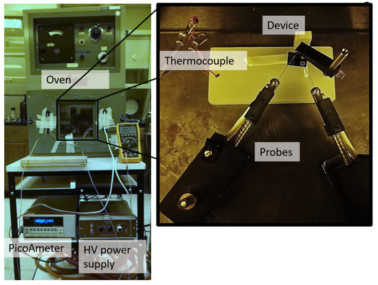
Figure 2.
The poling setup, with a view of the probe configuration inside the oven.
The device was placed in the oven, elevated to allow heating from both the top and the bottom, and connected with probes to a high voltage power supply. The oven was turned on and the device began to be heated to reduce thermal shock. When the temperature reached 50 °C. A DC voltage was applied across the device and heating continued until the oven reached 135 °C. The hold temperature of 135 °C ensures that the glass transition temperature of 135 °C is not exceeded while maximizing r33. At the glass transition temperature chromophores can move freely to orientate themselves in the direction of the applied electric field. Exceeding the glass transition temperature will result in dielectric breakdown, causing the device to electrically short, destroying the device. As soon as 135 °C was reached the heating element of the oven was switched off and the device was allowed to cool. Once the oven had cooled to 100 °C the oven was opened to facilitate rapid cooling. The voltage was turned off when the device was below 50 °C and then allowed to cool to room temperature. Leaving the voltage on while the device is cooling prevents the relaxation of chromophore alignment while the device is at an elevated temperature. Figure 3 shows the temperature and current data collected from poling with increasing poling voltage. The poling current is not correlated with the electro-optic coefficient, but it does indicate that charge moves more freely at elevated temperatures. Seeing a temperature-dependent current spike as the polymer approaches the glass transition temperature is a positive indication that the device is heating during the poling process as the resistivity of the polymer layers decrease with temperature.
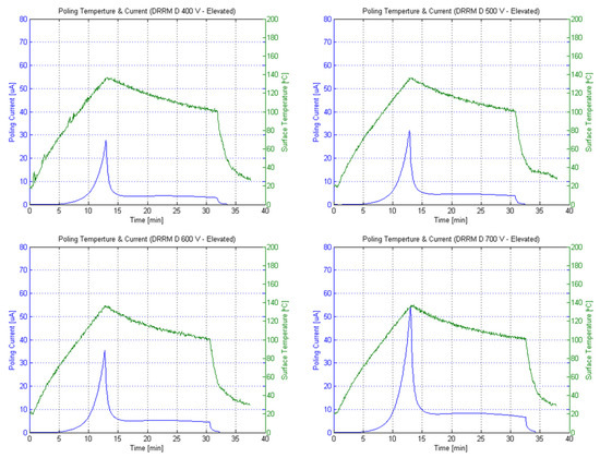
Figure 3.
Poling temperature (green) and current (blue) for a waveguide stack poled at 400 V, 500 V, 600 V, and 700 V.
5. r33 Measurement Setup
The r33 values of the poled devices were measured. A Mach-Zehnder interferometer (MZI) was constructed with optical fiber and the device was inserted into one leg of the MZI, the testing setup is shown in Figure 4. A 100 mW diode laser at 1545 nm was used for testing of the device. This power was split with 90% of the power to the device leg (to overcome waveguide losses and coupling losses) and 10% of the power within the reference leg. For the device leg, a polarization controller was inserted before the splitter, to ensure the light launched into the device was TM polarized. TM light was used because the fabrication process placed the electrodes above and below the waveguides. The polarization of the light is important as the r33 only effects the index of refraction in the direction the EO-polymer was poled. In order for this effect to be observed the light must be TM polarized. The TM polarized light was coupled into the single mode waveguide with a 6 µm PM fiber mounted on a three-axis XYZ micrometer stage. The output of the device was collected by a 9 µm PM fiber mounted on an identical three-axis XYZ stage. The reference leg first passed through a variable attenuator to allow for the power to be matched to that of the device leg. The variable attenuator can cause a change in polarization that must be corrected through a second polarization controller to match the device leg’s polarization. Both legs were then recombined in a 50/50 combiner and went to an optical power meter connected to an oscilloscope. A function generator was used to apply a triangular wave to the device. This signal was monitored on the oscilloscope as the optical power modulation was observed.

Figure 4.
The testing setup to measure the r33 of a poled polymer waveguide.
Data was collected for frequencies of 40 Hz, 100 Hz, 500 Hz, and 1k Hz using the oscilloscope. Figure 5 shows an example modulation to measure Vπ. Vπ was measured for each set of data and r33 values were calculated using Equation (2) [16].
where λ is the wavelength (1545 nm), d is the thickness of the core layer (2.7 µm), n is the index of refraction of the core (1.65) [6,13] and Γ is the overlap integral is 1 for vertically sandwiched electrodes because the entirety of the waveguide is covered by the uniform electric field. Vcore is the percentage of Vπ applied across the core layer, found to be 21% of the total field as described in Equation (1). L is the modulation length over which the voltage is applied which varied from 1.73 to 3.63 cm. Vπ is the change in voltage applied to the device required to change from maximum to minimum optical power. As previously described, Vπ was measured directly. From that measurement, r33 could be calculated using Equation (2). It is important to note that because only the electric field in the EO- polymer will contribute to the modulation, the voltage across the 2.7 μm of the core layer was found using Equation (1) and the resistivities of NOA 73 and SEO 100c. The poling, measurement, and calculation processes were repeated for multiple devices at various poling voltages ranging from 50 to 800 V.
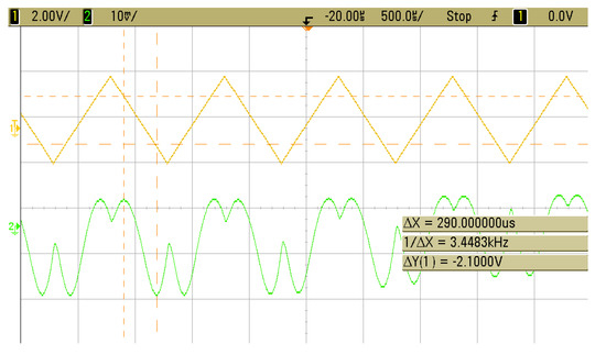
Figure 5.
Vπ measurement of the EO-waveguide from a MZI configuration showing a Vπ of 2.1 V. The top (yellow) wave form is the applied triangle wave, and the bottom (green) waveform is the optical modulation response.
6. Results
To evaluate the performance of the SEO100c polymer in a single mode waveguide, three variables were examined, poling electric field strength, poling temperature, and chromophore relaxation.
6.1. Poling Electric Field Strengh Results
Data was collected at four frequencies, 40 Hz, 100 Hz, 500 Hz, and 1k Hz. The presented r33 for each poling voltage is the average r33 of these four data points. The error bars were determined by calculating the standard deviation of the data set at each poling voltage. The resulting data show two distinct regions of r33 as a function of poling field: a non-linear region at low poling voltages (<25 V/μm across the EO core) and a linear region for higher poling voltages as shown in Figure 6. The r33 values obtained at the lower poling voltage resulted in a non-linear region. This effect has been attributed to there being insufficient voltage to overcome the resistance to chromophore movement in the poled device. This resistances of chromophore movement is caused by the chromophore being tangled within the host polymer [17,18]. The linear region shows an increase of 0.37 pm/V for every 1 V/μm of additional poling field strength. This trend can be extrapolated to find an r33 of 93 pm/V at 100 V/μm poling, which is the poling field specified by the data sheet to achieve the maximum r33 value. Higher voltages were avoided as they would increase the risk of device damage, and fields in excess of 77 V/μm would cause sparking damaging the top electrode.
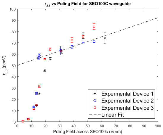
Figure 6.
Measured r33 for various polling field strengths. The dotted line shows a best fit linear line for poling fields greater than 20 V/µm across the core EO layer, with a slope of 0.37 pm/µm.
The value of 93 pm/V after being poled at 100 V/μm across the core, though high, is less than the value specified by the data sheet. The data sheet specifies an r33 of 140 pm/V for a wavelength of 1300 nm. Causes for this were investigated and it was found that though the measured air temperature was reaching 135 °C the device was only reaching 125 °C. This led to a slight alteration of poling process to study the correlation between poling temperature and r33.
6.2. Temperture Dependence on Poling Efficency
To examine the temperature dependence of the poling process, two samples were poled at 400 V for temperatures ranging from 120 to 135 °C. As with the r33 vs. poling voltage, the data presented in Figure 7 is the average measured r33 taken at modulation frequencies of 40 Hz, 100 Hz, 500 Hz, and 1k Hz. The error bars shown is the standard deviation of the data set. Figure 7 shows the results showing a clear increase in the r33 with an increase in poling temperature until saturation was reached at 135 °C. One note worth observation is that despite an insignificant change in the r33 between the 130 °C and 135 °C, the peak current through the device increased from 50 µA to 75 µA. This shows that the additional increase in temperature brought the device closer to dielectric breakdown without any beneficial effects to the r33 [19].
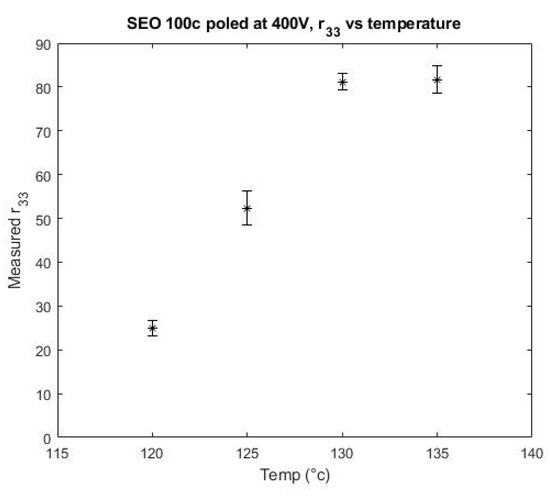
Figure 7.
An increased r33 for SEO100c is seen as the maximum poling temperature is increased.
6.3. Electro-Optic Stability over Time
In addition to examining the relation between the r33 and applied poling voltage, the stability of the r33 over time has been examined. The stability of the r33 over time is critical to ensure consistent results for experimental devices and is a significant hurdle for the use of polymers in commercial products. A device was poled at 800 V and the r33 was measured over time. Over a period of 65 days no significant relaxation of the r33 was observed with a device stored at room temperature. The device was tested at 40 Hz, 100 Hz, 500 Hz, and 1k Hz with the average of the measurements presented as each data point. The error was calculated by finding the standard deviation of the data set. The initial measurement taken immediately after poling showed an r33 of 74 pm/V, all subsequent measurements taken were within the standard deviation (+/−2.98 pm/V) or 4% of this initial measurement. Therefore, the electro-optic coefficient of SEO100c is stable for the first 65 days after poling. Figure 8 shows the evolution of SEO100c’s r33 value over time. Previously the stability of SEO100c’s EO coefficient has been observed over 30 days [20]. This experiment has extended the time over which SEO100c has been shown to have stable EO properties.
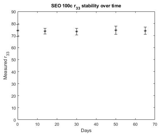
Figure 8.
The r33 stability of SEO100c over time.
7. Conclusions
Specific poling parameter behavior with respect to poling voltage, temperature, and long-term stability have been quantified. A non-linear relationship between the r33 and the strength of the poling voltage has been empirically measured and reported showing potential design and production pitfalls when assuming linear poling behavior. It has been shown that an r33 of 81 pm/V can be achieved without significant risk of dielectric breakdown in a SEO 100c waveguide device structure made from commercial polymers. For voltages in the linear poling region, the SEO100c polymer increases its r33 by 0.37 pm/V for every additional 1 V/μm applied to the device during the poling process. Up until the r33 saturation that occurs at the poling temperature of 130 °C, increasing the temperature at which the SEO100c polymer is poled increases the r33 of the EO-polymer. Increasing both the temperature and poling voltage increase the measured r33 value of EO waveguide devices in a non-linear behavior. In practice, poling conditions must also be empirically validated as it was shown that measuring the air temperature does not accurately reflect the device temperature. Additionally, the stability of SEO100c r33 has been shown for a two-month period.
Author Contributions
Conceptualization, M.M., E.G. and C.M.; Data curation, M.M. and C.M.; Formal analysis, M.M. and E.G.; Funding acquisition, C.M.; Investigation, M.M. and E.G.; Methodology, M.M., E.G. and C.M.; Project administration, C.M.; Resources, M.M. and C.M.; Supervision, C.M.; Validation, M.M. and E.G.; Visualization, M.M.; Writing—original draft, M.M.; Writing—review and editing, M.M., E.G. and C.M. All authors have read and agreed to the published version of the manuscript.
Funding
This research received no external funding.
Institutional Review Board Statement
Not applicable.
Informed Consent Statement
Not applicable.
Data Availability Statement
Data sets are available on request from the corresponding author.
Conflicts of Interest
The authors declare no conflict of interest.
References
- Breed, G. A Tutorial Introduction to Optical Modulation Techniques. Available online: http://www.highfreqelec.summittechmedia.com/May07/HFE0507_Tutorial.pdf (accessed on 13 April 2021).
- Corporation, L. Applications of Electro-Optic Polymers and Devices: Breaking the High Frequency, Broad Bandwidth Barrier; Lumera Corporation: Bothel, WA, USA, 2008. [Google Scholar]
- Marder, S.R.; Kippelen, B.; Jen, A.K.-Y.; Peyghambarian, N. Design and synthesis of chromophores and polymers for electro-optic and photorefractive applications. Nature 1997, 388, 845–851. [Google Scholar] [CrossRef]
- Enami, Y.; Luo, J.; Jen, A.K. Short hybrid polymer/sol-gel silica waveguide switches with high in-device electro-optic coefficient based on photostable chromophore. AIP Adv. 2011, 1, 042137. [Google Scholar] [CrossRef]
- Jouane, Y.; Chang, Y.; Zhang, D.; Luo, J.; Jen, A.K.; Enami, Y. Unprecedented highest electro-optic coefficient of 226 pm/V for electro-optic polymer/TiO2 multilayer slot waveguide modulators. Opt. Express 2014, 22, 27725–27732. [Google Scholar] [CrossRef] [PubMed]
- Briseno, M.J. Electro-Optic Contact Poling of Polymer Waveguide Devices and Thin Films. Ph.D. Thesis, Michigan Technological University, Houghton, MI, USA, 2017. [Google Scholar]
- Page, R.H.; Jurich, M.; Reck, B.; Sen, A.; Twieg, R.J.; Swalen, J.; Bjorklund, G.C.; Willson, C. Electrochromic and optical waveguide studies of corona-poled electro-optic polymer films. JOSA B 1990, 7, 1239–1250. [Google Scholar] [CrossRef]
- Teng, C.; Man, H. Simple reflection technique for measuring the electro-optic coefficient of poled polymers. Appl. Phys. Lett. 1990, 56, 1734–1736. [Google Scholar] [CrossRef]
- Dureiko, R.; Schuele, D.; Singer, K. Modeling relaxation processes in poled electro-optic polymer films. JOSA B 1998, 15, 338–350. [Google Scholar] [CrossRef]
- Zhang, C.; Wang, C.; Yang, J.; Dalton, L.R.; Sun, G.; Zhang, H.; Steier, W.H. Electric poling and relaxation of thermoset polyurethane second-order nonlinear optical materials: Role of cross-linking and monomer rigidity. Macromolecules 2001, 34, 235–243. [Google Scholar] [CrossRef]
- Herrera, O.D. Nonlinear Photonics in Waveguides for Telecommunications; The University of Arizona: Tucson, AZ, USA, 2014. [Google Scholar]
- Pogossian, S.P.; Vescan, L.; Vonsovici, A. The single-mode condition for semiconductor rib waveguides with large cross section. J. Lightwave Technol. 1998, 16, 1851–1853. [Google Scholar] [CrossRef]
- Gawron, E.; Maurer, M.; Middlebrook, C.; Kellar, K. Optical loss characterization of SEO100C electro-optic polymer within single mode rib waveguides. OSA Contin. 2019, 2, 3299–3308. [Google Scholar] [CrossRef]
- Hosseinzadeh, A. Linear Ring Resonator Modulator for Microwave Photonic Links. Ph.D. Thesis, Michigan Technological University, Houghton, MI, USA, 2018. [Google Scholar]
- Soluxra. Processing Decription of SEO100c; Soluxra: Kenmore, WA, USA, 2015. [Google Scholar]
- Nishihara, H.; Haruna, M.; Suhara, T. Optical Integrated Circuits; McGraw Hill Professional: New York, NY, USA, 1989; Volume 1. [Google Scholar]
- Enami, Y.; Derose, C.; Mathine, D.; Loychik, C.; Greenlee, C.; Norwood, R.; Kim, T.; Luo, J.; Tian, Y.; Jen, A.-Y. Hybrid polymer/sol–gel waveguide modulators with exceptionally large electro–optic coefficients. Nat. Photonics 2007, 1, 180–185. [Google Scholar] [CrossRef]
- Lynn, B.; Miles, A.; Mehravar, S.; Blanche, P.-A.; Kieu, K.; Norwood, R.A.; Peyghambarian, N. Real-time imaging of chromophore alignment in photorefractive polymer devices through multiphoton microscopy. MRS Commun. 2015, 5, 243–250. [Google Scholar] [CrossRef][Green Version]
- Sprave, M.; Blum, R.; Eich, M. High electric field conduction mechanisms in electrode poling of electro-optic polymers. Appl. Phys. Lett. 1996, 69, 2962–2964. [Google Scholar] [CrossRef]
- Makowska-Janusik, M.; Reis, H.; Papadopoulos, M.G.; Economou, I.; Zacharopoulos, N. Molecular dynamics simulations of electric field poled nonlinear optical chromophores incorporated in a polymer matrix. J. Phys. Chem. B 2004, 108, 588–596. [Google Scholar] [CrossRef]
Publisher’s Note: MDPI stays neutral with regard to jurisdictional claims in published maps and institutional affiliations. |
© 2021 by the authors. Licensee MDPI, Basel, Switzerland. This article is an open access article distributed under the terms and conditions of the Creative Commons Attribution (CC BY) license (https://creativecommons.org/licenses/by/4.0/).