1. Introduction
The rapid growth of smart devices that are interconnected over the internet has opened up new application fields such as wearables, smart home, smart grid, connected cars, and others. Therefore, the superior term Internet of Things (IoT) as a megatrend has gained more and more attention during the past few years. In general, the IoT includes a wide range of devices from simple interconnected sensors to complex systems as such mobile devices, vehicles, and smart labels, to name a few [
1,
2]. Interconnected devices carry sensitive data that can be a target of cyberattacks [
3]. Typical countermeasures include cryptographic methods, often based on random numbers used to generate public and private keys. At this point, one should note that a secret is just as trustworthy as its origin. For that reason, researchers started to use the random intrinsic variations of electronic circuits to generate unique and unclonable identifiers (IDs). These hardware-based security primitives are called Physical Unclonable Functions (PUFs) and have been introduced in recent works for authentication, identification, and cryptographic applications [
4,
5,
6]. One of the great advantages of PUFs is that there is no necessity for non-volatile memory, since the PUF generates keys on demand while being stimulated. The general behavior of a PUF includes a system’s unpredictable response
R, due to the intrinsic variations, with respect to the system’s input stimulus, namely the challenge
C, hence we can conclude
, where
f is not known and only influenced by the system or device-specific variations [
7,
8].
Many existing PUFs, such as ring oscillator (RO) [
9,
10,
11] and arbiter-based [
7,
12] designs, are complex and hard to integrate for device manufacturers into their application ICs, due to great design overheads or poor performance in security metrics. In the past years, analog-based PUF circuits have been proposed that use lower complexity circuit designs while achieving very good results in PUF security metrics. This property makes analog-based PUFs strong candidates as lightweight security primitives for constrained devices [
13].
In this work, we propose a real-hardware evaluation platform for an analog-based PUF, implemented in a highly scalable design. The herein presented PUF as an embedded system covers the entire software and hardware implementation and is verified through PUF security metrics as a viable PUF design. Due to the discrete device approach, reconstruction of the platform is of relatively low complexity compared to integrated circuit prototyping. This helps to enable applied research on a highly stable analog PUF and allows for experimentally embedding this PUF system into existing software frameworks at very low cost.
We provide the following contributions:
The PUF evaluation platform as a scalable design with low design complexity.
Detailed presentation of the peripherals and interfaces of the system.
Software design and fabrication of 30 PUF cores.
Experimental characterization and testing of internal analog voltages that are the basis of response bit generation and discussion of the reliability metric on the analog level.
Testing and evaluation of PUF security metrics including reliability, uniqueness, and bit errors in the temperature range of °C to 80 °C.
The remainder of this paper is structured as follows:
Section 2 and
Section 3 explain the related work and discuss the PUF design. The software and hardware implementation are addressed in
Section 4. In
Section 5, the security analysis and experimental results are shown and
Section 6 compares our work with related PUFs. Finally,
Section 7 concludes this paper.
2. Related Work
2.1. Classification of PUFs
Recent works have defined various classifications for PUFs that are based on how a PUF’s intrinsic variations are exploited for the response bit generation. The most commonly used classes divide into bi-stable or delay-based PUFs [
14,
15,
16,
17,
18,
19,
20,
21]. Other works also target the class of analog-based PUF designs [
22,
23,
24,
25,
26]. A further classification relies on the complexity of the challenge–response mechanism, more particularly on the number of challenge–response pairs (CRPs). PUFs that exhibit a small CRP space are called weak PUFs, often used in a controlled PUF configuration to extract secret keys. PUFs providing a large CRP space are referred to as strong PUFs.
2.2. Related PUF Designs
A first approach for analog-based PUFs was presented by Lofstrom et al. in [
22]. In their work, a cell array of identical small-gate transistors sequentially addresses a resistive load that generates an output bit-sequence depending on the device’s output voltage levels.
In another work, Sehwag et al. [
23] presented the Threshold Voltage PUF (TV-PUF), using a cascading method to increase small differences of threshold voltage variations in pass-transistors in order to exploit its cumulated impact on the output voltage.
A hardware realization of transmission gate (TG) based analog PUFs, the Transmission Gate PUF (TG-PUF), incorporating and measuring voltage drops across transmission-gate transistors, was introduced in [
24].
Another inverter-based PUF has been proposed in [
25], where the main focus relies on exploiting the inverter’s nonlinear output characteristics and cascading multiple blocks in series, making the PUF more resilient to machine learning attacks in comparison to delay-based PUFs.
In [
26], an analog-based PUF structure uses a CMOS architecture with biasing at the point of maximum DC-gain, exploiting complementary inverter threshold voltage
variations.
Development boards with respect to hardware security can be deployed for digital PUFs such as the HECTOR development board [
27] or the SASEBO board [
28].
To the best of our knowledge, almost all of the published works so far have either been simulated, implemented on FPGAs, or fabricated as stand-alone chips and hence have not been characterized to show their inherent properties such as voltage at critical nodes for the functionality of the PUF design. Usually, when voltage levels at critical nodes are not known, instabilities in the response need to be computed solely based on the binary bit values of the response. The usage of analog-to-digital converters (ADCs) on these critical nodes allows for investigation of the voltages that lead to bit generation. Based on the gained knowledge, thresholding techniques for robust bit generation can be explored and deployed. To conduct further application-based research on any of the existing analog PUFs, the designs have to be reconstructed and the prototype chip further investigated.
The presented work in this paper provides a building block for researching a scalable analog-based PUF design, enabling security evaluation and optimization. In general, the proposed discrete PUF design tackles typical shortcomings of chip-based PUFs which are higher initial fabrication costs, longer production times, and less accessibility as needed in a research environment.
3. Proposed PUF Design
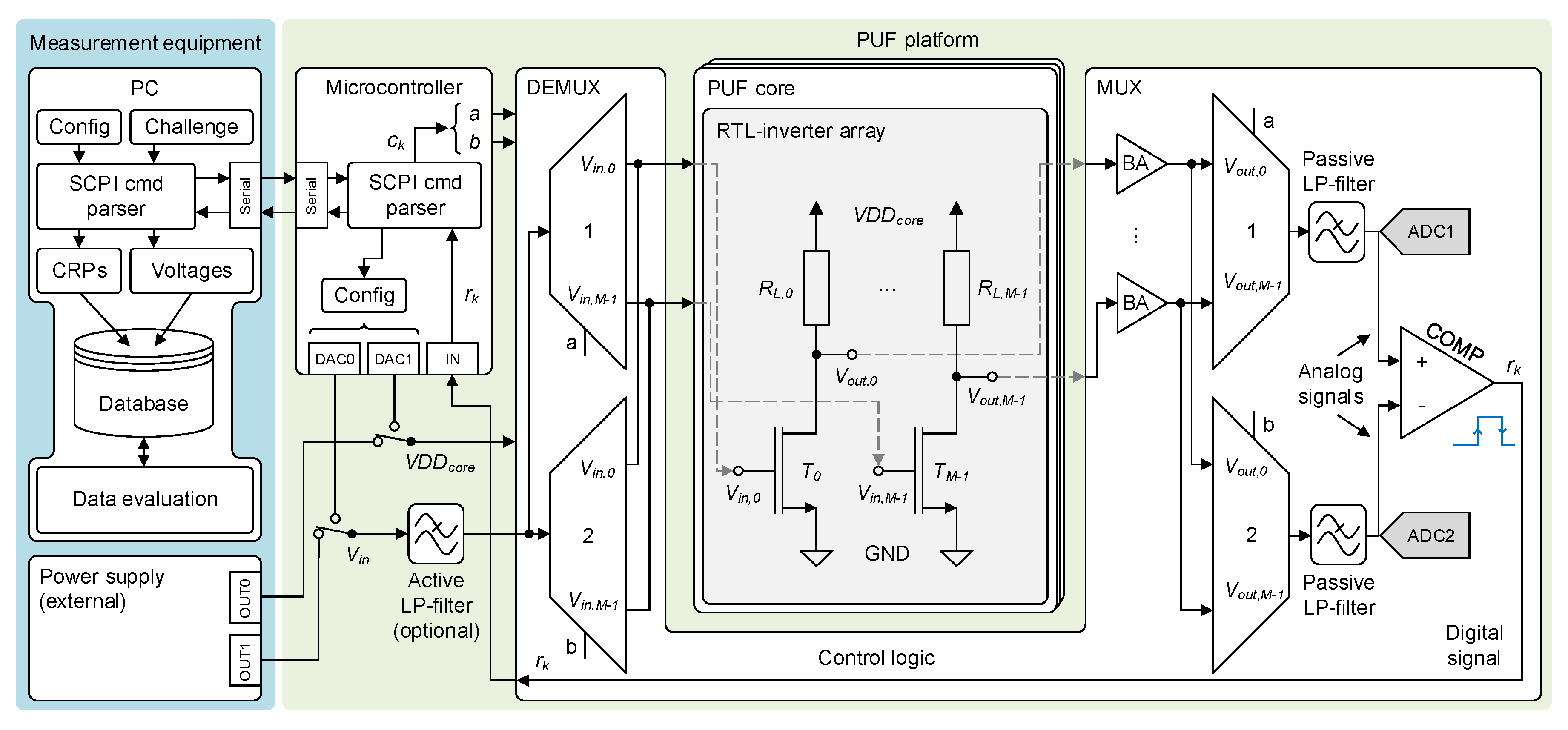
Our proposed PUF platform, as shown in
Figure 1, consists of a microcontroller, the control logic (also referred to as Evaluation Board), and the PUF core.
The platform enables direct access to the analog PUF in a full discrete board-level design, especially designed for the used PUF core fabricated with
inverters. Furthermore, the proposed PUF allows nonlinear bit-width scaling by increasing the number of PUF core inverters, comparable to related PUF architectures as, e.g., RO-PUFs [
5].
Each PUF core inverter is realized with a commercially available NMOS-transistor
T and a resistive load
with 1% variation. The sequential addressing process selects two inverters in parallel. Due to process variations, the transistor drain currents
differ slightly [
29]. In combination with the impact of resistive loads, this results in a variation of the inverter’s output voltage
. The PUF core inverters are set up such that
with
, ensuring that the transistors operate in the active region for nominal devices.
For signal routing, a constant input biasing voltage
is fed to the system.
is routed to the two addressed inverter input terminals via two bi-directional multiplexers (MUXs), used as demultiplexers (DEMUXs), as shown in the middle part of
Figure 1. Each PUF core inverter output voltage
is buffered by a voltage-follower configured operational amplifier (op-amp) to separate the intrinsic variation source from the readout circuitry. Each buffered output voltage is routed to its corresponding MUX input channel in both MUXs. Therefore, the same bi-directional multiplexers as for demultiplexing are deployed. The MUX1 output signal is routed to the positive comparator input terminal and ADC channel 1, respectively. The output of MUX2 is routed to the negative comparator input terminal and ADC channel 2, as shown in
Figure 1. Each readout path utilizes a first-order RC low-pass filter around a cut-off frequency of
, which limits the signal-bandwidth of the readout path.
3.1. PUF Challenge and Response
In general, a challenge
C is composed of a set of sub-challenges, whereas one sub-challenge
consists of two inverter addresses
and the inverter input biasing voltage
. Equation (
1) defines the resulting sub-challenge tuples, where
denotes the
k-th sub-challenge of
C. Furthermore,
denotes the sub-response of
and the
k-th sub-response of
R:
Basically, two arbitrary inverter addresses
a and
b can either be arranged in the combination
or
. Due to the definition of the sub-challenge
(see Equation (
1)), for each pair of inverter addresses, one response bit
is produced. When reversing
to
, the binary value of response bit
should change to
. This coherence can be used in a system test in order to detect defective inverters. When determining the maximum response bit width
, such reversed addresses are omitted in PUF, since they would degrade the self-information in proportion to the absolute bit width. Thus, the condition
must be valid for all sub-challenges. For
M inverters, the maximum response bit width
is determined by the binomial coefficient, as shown in Equation (
2):
3.2. Systematic Variation Decomposition
For the further discussion, we define the general statement for the inverter’s varying output voltage
with
, which represents a sub-response
of two arbitrarily addressed inverters (see
Figure 2a).
The input voltage of the inverters at its input terminals is
. Nonetheless, due to possible offset voltages in the biasing path, the input voltages might differ slightly. This would introduce another systematic error directly affecting
. For our system, this possible effect would be marginal and is therefore disregarded in the following discussion. Furthermore, the output voltages are forwarded to the comparator terminal positive (
p) and negative (
m) inputs (see
Figure 2a), namely
with
, which is shown in Equation (
3):
Here,
describes the sum of systematic error voltages, caused due to the readout path of the inverter array with
, where
denotes a normal distribution. Due to the PUF’s differential approach, fluctuations of the PUF core’s supply voltage
and its impact on
are suppressed, keeping
constant over the time
t of operation [
30].
4. Software and Hardware Evaluation System
This section explains the software implementation of the microcontroller firmware of the PUF evaluation system. Furthermore, the modular design of the fabricated hardware platform is shown.
4.1. Software Design
The PUF platform can be fully controlled by the user from a PC via a serial communication interface. Similar to existing measurement instruments, the Standard Commands for Programmable Instruments (SCPI) protocol [
31] is used to send commands to the evaluation platform. The user can configure the microcontroller software and set the PUF’s operating conditions (
and
). Additionally, the timing of the PUF response generation procedure can be defined through the
and
parameters, which also affect the ADC sampling time, as shown in
Figure 2b.
Figure 3a shows the program flow as a state machine for sending PUF challenges including ADC measurements. The software on the microcontroller behaves as shown in
Figure 3b and is fully sensitive regarding incoming SCPI commands. The microcontroller subsequently controls the DEMUX/MUX circuits according to the addresses included in the sub-challenge
. The corresponding inverter input biasing voltage
is routed towards the two selected inverter input terminals. Additionally, the two addressed inverter outputs are routed towards the comparator input terminals, as shown in
Figure 1. The voltages at both comparator input terminals are tracked via an ADC. Finally, the ADC values and the sub-response
are sampled by the microcontroller. This procedure is repeated until all sub-challenges are processed and the full-length PUF response is generated. The microcontroller sends the binary PUF response and the corresponding ADC values to the PC.
4.2. Hardware Platform
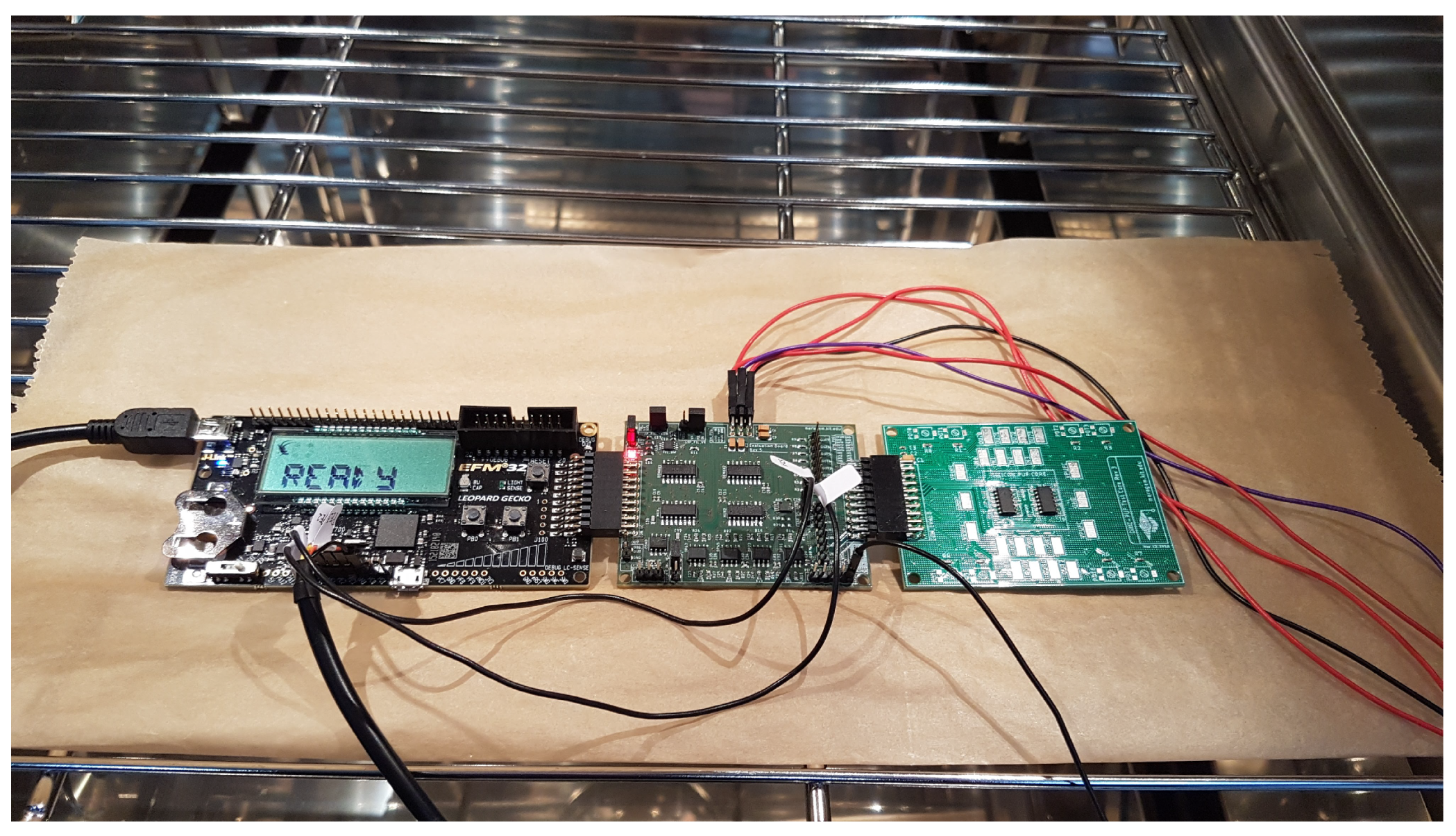
The entire PUF evaluation platform consists of the PUF circuits and a microcontroller (EFM32 Leopard Gecko development board) used for PC communication, challenge addressing, and PUF response readout. The PUF core design is kept modular such that single core entities are detachable, allowing interchangeability of core circuits for large-scale characterization.
Figure 4 shows the system operating in a climatic chamber (Weiss WK3).
5. Security Analysis
For the empirical evaluation of the PUF security metrics, we fabricated 30 PUF cores, extracted the binary PUF responses, and measured the corresponding analog output voltages under the impact of changing operating conditions.
Table 1 shows all test cases applied in our experiments.
The supply voltages of the PUF control logic peripherals , , and are provided by a Keithley HM80403 triple power supply. We calculate the reliability, uniqueness, and bit errors using the following procedure:
Step 1: Reference challenge. A fixed reference challenge is generated, consisting of all combinations of inverter addresses emitted in lexicographic order without repetitions.
Step 2: Reference response. For each PUF core instance, a reference response is extracted by applying the reference challenge under nominal operating conditions. The reference response is defined by determining the most occurring bit sequence out of a set of 125 PUF responses measured during the enrollment phase.
Step 3:
Data acquisition. As shown in
Table 1, for all test cases, each PUF core instance is evaluated 125 times under the stated operating conditions and its responses are stored in a database.
Step 4: Analysis. In terms of PUF security analysis, the reliability, uniqueness, and bit errors across all measured PUF cores are computed. Furthermore, by performing analog voltage measurements with all PUF cores, the impact of voltage variations on the PUF metrics is investigated.
5.1. Reliability Analysis
The reliability metric is a crucial factor in providing a robust outcome under environmental variances and disturbances, keeping a PUF response stable by minimizing the need for post-processing due to software-sided error correction [
11]. The reliability
for PUF instance
n is calculated on the digital output level, as stated in Equation (
4) [
32]:
where
describes the reference response at nominal conditions, meaning the nominal supply voltage and ambient temperature conditions at room temperature, whilst
describes the PUF response for
T different ambient conditions and different supply voltages. The response bit width is
and the ideal value for reliability is 100% [
32].
To decompose the response on the analog level, we look at the reliability solely based on the Hamming distance
, as shown in Equation (
5) for sub-response
. Thereby,
and
define bit strings of equal length
that are compared bitwise against each other:
Furthermore, we define states for voltages
and
according to Equations (
6) and (7), resulting in Equation (8):
The sub-response generated by the comparator is given as:
The maximum reliability (with
) of the PUF is therefore achieved for the cases
:
This emphasizes the necessity of a design level co-optimization between the minimization of the readout path’s error voltage
and its impact on the actual compared voltage at
along with the maximization of
[
9,
20,
33]. These constraints help to reduce unstable or even false detected bits already at design level. As for the error voltages, the best case would be
. Nonetheless, this case remains unlikely for our system, as the comparator’s input offset voltage limits the safely detectable voltage difference. However, to obtain a high similarity in each readout path for our system, resistors with equal temperature coefficients and low variation are incorporated. Moreover, the effect of leakage currents and resulting offset voltage errors are kept as low as possible. The deployed comparator has low input offset voltage and low input leakage currents, thus resulting in a systematic minimization of the error induced by the control logic.
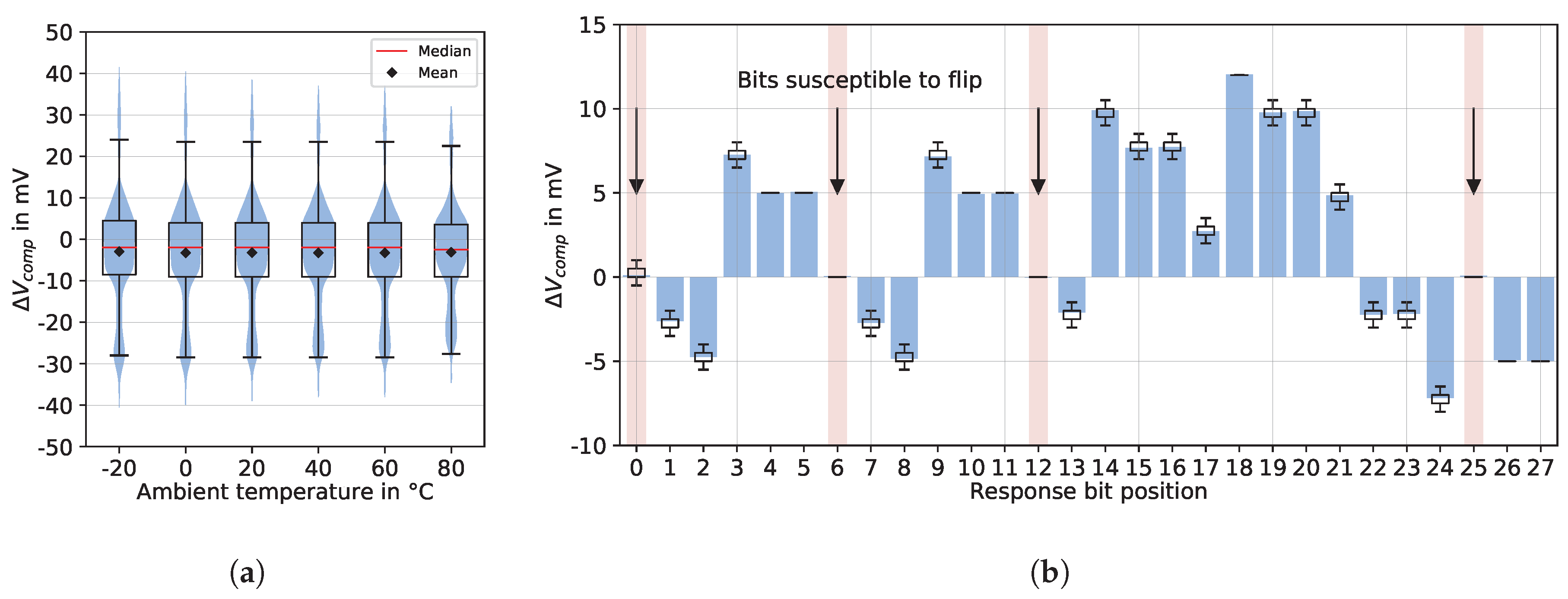
The experimental measurement data of the voltage difference at the comparator input terminals
over the specified temperature range (test cases
to
) of ten PUF cores is visualized in
Figure 5a. The data shown in this plot corresponds to the voltage differences reached at each temperature level, readout over 125 challenge–response cycles, which already provides sufficient statistics for a narrow distribution of the reliability metric discussed later in this paper (see
Figure 6). The main data distribution of
along the interquartile range (IQR) remains highly stable at
over the full measured temperature range. This shows the PUF’s good resilience over temperature, thus achieving high reliability on the analog signal level.
To gain insight into unstable responses, we plot
of PUF core 20 over all response bits, as shown in
Figure 5b. The bit positions
,
,
, and
show small absolute values for
of less than 200
, directly degrading reliability. As there is a chance that the output bits are biased towards an output direction (logical 0 or 1) due to the comparator’s input offset voltage and, being kept stable, thus generating a false output, or if both comparator input voltages are inflicted due to noise, the comparator output is susceptible to showing flipping behavior.
On the digital level, the evaluation of the binary responses by means of Equation (
4) results in an average reliability of
%.
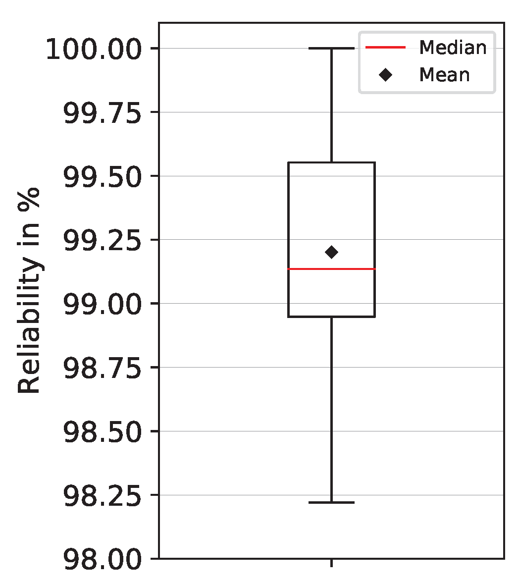
Figure 6 shows the reliability distribution for ten measured PUF cores, after performing test cases
to
. All cores show reliabilities close to the ideal value of 100%.
5.2. Uniqueness Analysis
In general, the uniqueness metric is a measure of how uncorrelated PUF responses are across different instances. When applying the same input challenge to various PUF circuits of equal type, ideally all responses should differ. We use the uniqueness metric introduced by Maiti et al. in [
32]. For two different PUF instances
i and
j, each having
L-bit (
) responses
and
, the uniqueness (or inter-device HD) for
devices is defined as:
The ideal value for uniqueness is 50%, indicating that all PUF responses are distinguishable.
We have assembled 30 PUF cores in total to evaluate the uniqueness metric as defined in Equation (
9). We applied a fixed challenge (full readout) to all PUF instances and measured their responses. We evaluated
-bit PUF responses from independent PUF core hardware instances under nominal conditions (test case
) using the Evaluation Board A. The average uniqueness and standard deviation are
and
, respectively.
Figure 7 shows the distribution of the uniqueness among the evaluated PUF cores. We repeated the measurements by utilizing a second Evaluation Board B, which is an identically constructed counterpart of Evaluation Board A. The results yield a mean of
and variance of
, which is identical to the results achieved with Evaluation Board A. The cross validation shows that the uniqueness is independent from the Evaluation Board used for PUF core addressing and readout, which is consistent with our assumption and intended design. The resulting uniqueness values are close to the ideal value of 50%.
5.3. Uniformity Analysis
The uniformity metric is an indicator for the balance of ’0s and ’1’s in the PUF response bits. Ideally, both binary values should occur equiprobable in a PUF response [
32]. For PUF instance
n, having an
L-bit (
) response
at bit position
l, the uniformity is defined as:
For our analysis, we used the reference responses of 30 fabricated PUF cores measured in our uniqueness evaluation. We computed the uniformity value for each PUF core and response with respect to Equation (
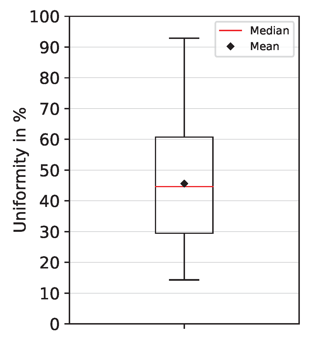
10). The resulting mean uniformity is 45.60%, which is close to the ideal value of 50%.
Figure 8 shows the box plot for all measured PUF responses. In general, a uniformity value lower than 50% means that the response is biased towards 0. The results for the uniformity are consistent with our analysis on the analog voltage level, where the mean value for the comparator input voltage difference is slightly negative, as shown in
Figure 5a.
Identification, which is one subgroup in the field of security, mainly relies on unique identifiers. In the ideal case, the entire binary address space for a given bit width can be used for distinction between single instances. In this context, the uniqueness metric shows how distinguishable the PUF responses are. In the context of cryptographic key derivation, the PUF response bits should be uniformly distributed. The greater the deviation from 50%, the easier to guess the response by an attacker. Our results show that the mean uniformity is around the ideal value. However, there are some PUF responses that are non-uniform, which makes the proposed PUF’s raw responses a candidate for identification applications, rather than for deriving cryptographic keys.
5.4. Bit Error Analysis
A bit error is a bit that flips between the binary values 0 and 1, when generating it multiple times consecutively. Such bit flips degrade both the reliability and uniqueness metrics. We have already discussed this coherence before in our reliability investigations. However, when evaluating fabricated PUFs, very often it might be useful to investigate the bit errors/flips that occur due to ambient temperature changes or supply voltage fluctuation over time. For that reason, we calculate the bit errors in percent for each PUF core that occurred during repeated response measurements. The bit error
for PUF instance
n is defined as the sum of all
s between its reference response
and
W measured responses
for the same reference challenge, both of the length
:
This metric can be considered as an extension of reliability and uniqueness evaluation. Hereby, bit errors can be investigated and made visible easier when analyzing PUF responses core by core.
Even when using a differential bit generation approach as in our PUF, bit errors might still occur due to changing environmental conditions and random noise. In some cases, the comparator input voltages differ very slightly, which potentially results in bit flipping over time, directly causing degradation of the reliability and uniqueness metrics. When using PUFs for unique ID generation, i.e., in identification applications, a typically applied approach is to define a binning technique in order to distinguish between individual IDs. The higher the amount of flipped bits within an ID, the less the uniqueness. As a consequence, low uniqueness leads to enlarged bins in the binning model. For that reason, we evaluate bit errors of PUF across the ambient temperature range from
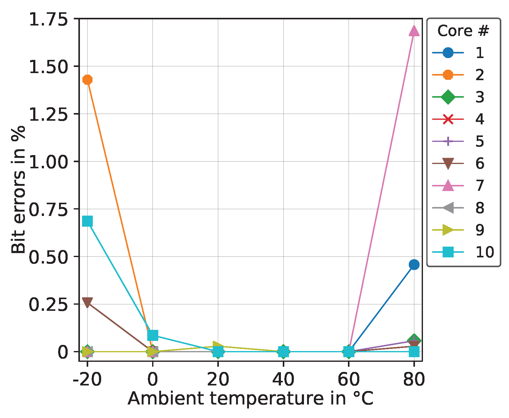
°C to 80 °C in 20 °C steps. We measured 125 responses per core by applying a fixed reference challenge (full readout) to the PUF.
Figure 9 shows the bit errors in percent for 10 PUF cores measured in a climatic chamber (test cases
to
). The plot shows increased bit error values at
°C and 80 °C for certain PUF cores, which denotes the maximum ratings in terms of operating temperature. Core 9 shows a slightly increased bit error value at 20 °C. This can be explained by the corresponding voltage measurements at the comparator input terminals. The voltage difference
for bit position
differs only a little and sometimes turns from positive to negative (flipping between logical 0 and 1).
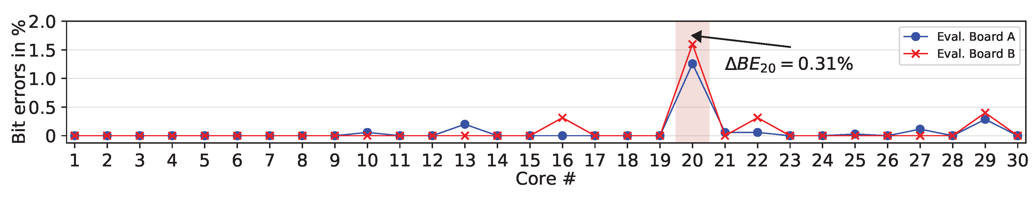
In a second experiment, we explored the bit errors independent of the evaluation board used. Therefore, we measured 30 physical PUF core instances at nominal conditions (test case
) by utilizing two Evaluation Boards A and B, respectively.
Figure 10 shows the corresponding bit error values. Core 20 shows the greatest bit errors, which we have already explained in our reliability discussion earlier in this paper. The bit errors remain almost stable if comparing the measurements for both Evaluation Boards with each other. Moreover, core 16 shows the maximum deviation between Evaluation Board A and B with
, which is still below 0.5% and hence negligible low.
5.5. Discussion on Security Threats
In the past few years, many PUF designs have been successfully attacked using machine learning (ML) techniques. Thereby, attackers focus on strong PUFs offering a large CRP space [
34,
35,
36]. The goal of the attackers is to construct a mathematical clone which behaves like the original PUF. CRPs are eavesdropped during normal operation of the PUF to gather a data basis for model training. However, a full readout of a strong PUF is often not possible due to the huge CRP space. Therefore, the goal is that only a subset of the CRP space must be eavesdropped and is sufficient to gain a trained model that is highly predictive in terms of estimating other not yet occurred CRPs.
From an attacker’s point of view, the herein presented analog PUF is comparable to the ring oscillator architecture, due to their similarities of the internal pairwise selection circuitry and bit generation. In the presented configuration, our design forms a weak PUF with just a single CRP. In general, applying modeling attacks is not applicable in the context of weak PUFs, since the data basis for model training is small. For that reason, a full readout of the PUF is more appropriate.
With regard to cryptographic key derivation, the uniformity of the PUF response bits is connected with the unpredictability of the responses. If the PUF response bits are biased towards 0 or 1, it is easier for an attacker to guess the response. In general, the assumed distributions of noise and PUF responses is often normal rather than uniform [
37]. This connotes a potential security threat for the herein proposed analog PUF. To counter this issue, fuzzy extractors can be used to generate unique keys suitable for cryptographic applications [
38,
39]. To protect the challenge and response interfaces from the outside world, weak PUFs are often surrounded by additional obfuscation logics such as hash functions. This configuration is often referred to as controlled PUF [
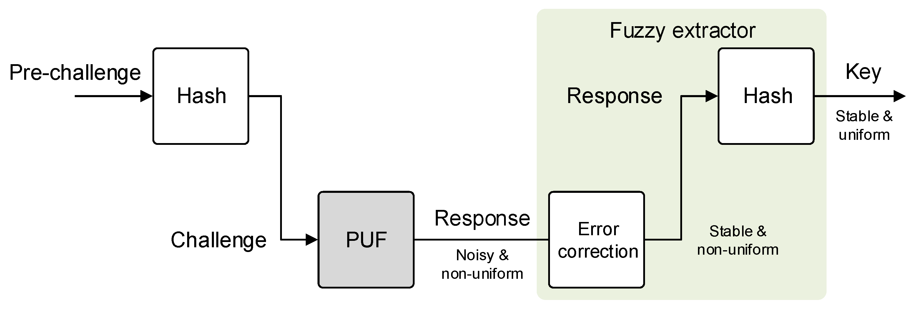
40].
Figure 11 shows how to turn the proposed weak PUF into a controlled PUF environment, also including a fuzzy extractor to generate stable and uniform keys, e.g., for cryptography.
However, when scaling up the herein presented analog PUF circuit, the CRP space can also be increased and the PUF becomes a candidate for a strong PUF design. As a consequence, the investigation of modeling attacks becomes more attractive to spot vulnerabilities towards the PUF’s unpredictability and physical unclonability. In this context, commonly used attack scenarios come into account, such as side-channel attacks to eavesdrop CRPs [
41]. In the next step, these CRPs can be used to train a mathematical model of the PUF’s internal behavior using machine learning techniques. Another option is to create a sorted list of PUF core inverter output voltages, similar to the approach proposed for RO-PUFs by Ruehrmair et al. in [
42].
In this paper, the focus lies on the design, fabrication, and evaluation of an analog PUF platform. Therefore, performing and discussing modeling attacks on the presented analog PUF design in more detail will be part of our future work.
6. Comparison to Other Designs
As mentioned in the introduction of this paper, analog-based PUF designs benefit from relatively simple circuit designs, which make them suitable for the integration into IoT devices that are mostly bound to hard requirements such as being small-sized, low-cost and having limited resources. Various analog-based PUF designs have been reported earlier by other working groups [
22,
23,
24,
25,
26]. In the following, we provide a closer look at other analog-based PUFs, similar to our system.
The TV-PUF [
23] uses two parallel blocks with cascaded pass-transistors. Cascading helps to accumulate the impact of
variation per pass-transistor, which is subtracted from
over the amount of pass-transistor stages. A static voltage sense comparator is used to compare the voltage levels between the two activated blocks’ output voltages and to generate a bit. The design is simulated and verified using 45
, 65
, and 90
technology processes.
The TG-PUF [
24] utilizes a stimulus/measurement circuit (STM) which consists of 20 ’pseudo’ pass gates, referred to as transmission gate (TG) [
24]. An output voltage is generated, caused by a voltage drop over a TG, due to the devices’ on resistance
, which is addressed by a selection circuitry. Furthermore, a voltage-to-digital converter (VDC) is used to sense the generated output voltages. The design generates voltage differences which are utilized to generate bit-strings. Thresholding techniques are proposed and applied to generate stable bit responses. The design is fabricated and verified using a 90
technology process.
The VTC-PUF [
25] exploits staging of circuit blocks over 64 switches. The VTC circuit block consists of an inverter and a feedback transistor, which prevents the inverter output to swing either to the circuits
or ground. The design uses two blocks as a pair. The switches act as a challenge and route the output of the blocks to the according next stage inputs. A voltage sense amplifier, attached to the last block, is used to compare the staged output voltage differences and generates a bit. This design is more robust against several ML algorithms in comparison to delay-based PUF architectures such as Arbiter PUFs, due to the cascading of nonlinear inverter characteristics. The design is simulated and verified using a 45
technology process.
Table 2 shows the reliability, uniqueness, and uniformity metrics for related PUFs and the proposed PUF platform (bold).
One should note that the reliability metric evaluations for the different PUF shown in
Table 2 have been carried out under various temperature ranges. The smallest temperature range was used for VTC-PUF, reaching from 0 °C to 85 °C. All other works, also including the herein proposed evaluations, additionally applied negative temperatures to their PUF circuits. The direct comparison of the reliability metrics shows that our fabricated PUFs produce highly reproducible responses, even under extreme environmental conditions.
In terms of the uniqueness metric, our evaluation results indicate that the PUF responses are unique, which in connection with the superior reliability value qualifies the proposed design for identification purposes. However, the uniformity analysis shows that additional effort has to be spent for pre- and post-processing techniques—as, for instance, additional hash functions and a fuzzy extractor, to make the PUF responses ready for cryptographic applications.
Altogether, our proposed design shows statistics in the performance metrics close to the ideal values. Therewith, the PUF platform accomplishes the security-related requirements for PUF designs in addition to its unique benefits of accessibility and bitwise understanding on analog and digital signal levels. Because of the low design complexity of the herein proposed analog-based PUF platform, the PUF design is a strong candidate as a lightweight security primitive.
7. Conclusions
In this paper, we introduced a holistic evaluation platform for an analog-based Physical Unclonable Function (PUF), covering the full software and hardware implementations. We fabricated 30 PUF cores and evaluated their PUF responses under different operating conditions, such as changing ambient temperatures and varying supply voltages. Due to the additional measurement capabilities of our evaluation platform, we could trace PUF response bit flips that occurred on the digital level back to the analog voltage level. Furthermore, we evaluated the bit errors that appear over time for each single PUF core. The experimental results of the fabricated PUF core instances show superior security metrics, such as an average reliability of 99.20%, a uniqueness value of 48.84%, a uniformity of 45.60%, and low bit error rates. In addition, our PUF platform offers the unique benefits of accessibility and bitwise understanding on analog and digital signal levels. These features make the proposed design highly suitable as an analog PUF test platform for hardware-centric security. In general, analog PUF designs as proposed in this work are promising candidates for the use in application fields where devices underlie strict design or performance constraints, such as in the IoT.
Author Contributions
Conceptualization, all; methodology, A.S. (Alexander Scholz) and L.Z.; software, L.Z.; validation, A.S. (Alexander Scholz) and L.Z.; formal analysis, A.S. (Alexander Scholz) and L.Z.; investigation, A.S. (Alexander Scholz) and L.Z.; resources, all; data curation, A.S. (Alexander Scholz) and L.Z.; writing—original draft preparation, A.S. (Alexander Scholz) and L.Z.; writing—review and editing, all; visualization, A.S. (Alexander Scholz) and L.Z.; supervision, A.S. (Axel Sikora), M.B.T., and J.A.-H.; project administration, A.S. (Axel Sikora), M.B.T., and J.A.-H.; funding acquisition, A.S. (Axel Sikora), M.B.T., and J.A.-H. All authors have read and agreed to the published version of the manuscript.
Funding
This research was funded by the Ministry of Science, Research, and Arts of the state of Baden Wuerttemberg, Germany.
Acknowledgments
This work was supported in part by the Ministry of Science, Research, and Arts of the State of Baden Wuerttemberg, Germany through the Modellierung, Entwurf, Realisierung und Automatisierung von gedruckter Elektronik und ihren Materialien (MERAGEM) Doctoral Program and in part by the Institute of Reliable Embedded Systems and Communication Electronics (ivESK), University of Applied Sciences Offenburg, Germany. The article processing charge was funded by the Ministry of Science, Research, and Arts of the State of Baden Wuerttemberg, and the Offenburg University of Applied Sciences in the funding program Open Access Publishing.
Conflicts of Interest
The authors declare no conflict of interest.
Abbreviations
The following abbreviations are used in this manuscript:
| ADC | Analog-to-digital converter |
| BA | Buffer amplifier |
| CMOS | Complementary metal-oxide-semiconductor |
| CRP | Challenge-response pair |
| DAC | Digital-to-analog converter |
| DC | Direct current |
| DEMUX | Demultiplexer |
| HD | Hamming distance |
| IC | Integrated circuit |
| ID | Identifier |
| IoT | Internet of things |
| MUX | Multiplexer |
| NMOS | Negative channel metal-oxide-semiconductor |
| PCB | Printed circuit board |
| PUF | Physical unclonable function |
| RO | Ring oscillator |
| SCPI | Standard Commands for Programmable Instruments |
| TG | Transmission gate |
| TV | Threshold voltage |
| VDC | Voltage-to-digital converter |
| VTC | Voltage transmission characteristics |
References
- Gubbi, J.; Buyya, R.; Marusic, S.; Palaniswami, M. Internet of Things (IoT): A vision, architectural elements, and future directions. Future Gener. Comput. Syst. 2013, 29, 1645–1660. [Google Scholar] [CrossRef]
- Chen, B.; Willems, F.M. Secret key generation over biased physical unclonable functions with polar codes. IEEE Internet Things J. 2018, 6, 435–445. [Google Scholar] [CrossRef]
- Keoh, S.L.; Kumar, S.S.; Tschofenig, H. Securing the internet of things: A standardization perspective. IEEE Internet Things J. 2014, 1, 265–275. [Google Scholar] [CrossRef]
- Gassend, B.; Clarke, D.; Van Dijk, M.; Devadas, S. Silicon physical random functions. In Proceedings of the 9th ACM Conference on Computer and Communications Security; ACM: New York, NY, USA, 2002; pp. 148–160. [Google Scholar]
- Suh, G.E.; Devadas, S. Physical unclonable functions for device authentication and secret key generation. In Proceedings of the Design Automation Conference, San Diego, CA, USA, 4–8 June 2007; pp. 9–14. [Google Scholar]
- Gassend, B.; Lim, D.; Clarke, D.; Van Dijk, M.; Devadas, S. Identification and authentication of integrated circuits. Concurr. Comput. Pract. Exp. 2004, 16, 1077–1098. [Google Scholar] [CrossRef]
- Hori, Y.; Yoshida, T.; Katashita, T.; Satoh, A. Quantitative and statistical performance evaluation of arbiter physical unclonable functions on FPGAs. In Proceedings of the 2010 International Conference on IEEE Reconfigurable Computing and FPGAs (ReConFig), Quintana Roo, Mexico, 13–15 December 2010; pp. 298–303. [Google Scholar]
- Herder, C.; Yu, M.D.; Koushanfar, F.; Devadas, S. Physical unclonable functions and applications: A tutorial. Proc. IEEE 2014, 102, 1126–1141. [Google Scholar] [CrossRef]
- Maiti, A.; Casarona, J.; McHale, L.; Schaumont, P. A large scale characterization of RO-PUF. In Proceedings of the 2010 IEEE International Symposium on Hardware-Oriented Security and Trust (HOST), Anaheim, CA, USA, 13–14 June 2010; pp. 94–99. [Google Scholar]
- Gao, M.; Lai, K.; Qu, G. A highly flexible ring oscillator PUF. In Proceedings of the 51st Annual Design Automation Conference; ACM: New York, NY, USA, 2014; pp. 1–6. [Google Scholar]
- Maiti, A.; Schaumont, P. Improving the quality of a physical unclonable function using configurable ring oscillators. In Proceedings of the International Conference on Field Programmable Logic and Applications, Prague, Czech Republic, 31 August–2 September 2009; pp. 703–707. [Google Scholar]
- Machida, T.; Yamamoto, D.; Iwamoto, M.; Sakiyama, K. Implementation of double arbiter PUF and its performance evaluation on FPGA. In Proceedings of the The 20th Asia and South Pacific Design Automation Conference, Chiba, Japan, 19–22 January 2015; pp. 6–7. [Google Scholar]
- Babaei, A.; Schiele, G. Physical unclonable functions in the Internet of Things: State of the art and open challenges. Sensors 2019, 19, 3208. [Google Scholar] [CrossRef] [PubMed]
- Chen, Q.; Csaba, G.; Lugli, P.; Schlichtmann, U.; Rührmair, U. The bistable ring PUF: A new architecture for strong physical unclonable functions. In Proceedings of the 2011 IEEE International Symposium on Hardware-Oriented Security and Trust (HOST), San Diego, CA, USA, 5–6 June 2011; pp. 134–141. [Google Scholar]
- Clark, L.T.; Medapuram, S.B.; Kadiyala, D.K.; Brunhaver, J. Physically Unclonable Functions Using Foundry SRAM Cells. IEEE Trans. Circuits Syst. I Regul. Pap. 2019, 66, 955–966. [Google Scholar] [CrossRef]
- Garg, A.; Kim, T.T. Design of SRAM PUF with improved uniformity and reliability utilizing device aging effect. In Proceedings of the 2014 IEEE International Symposium on Circuits and Systems (ISCAS), Melbourne, VIC, Australia, 1–5 June 2014; pp. 1941–1944. [Google Scholar]
- Morozov, S.; Maiti, A.; Schaumont, P. An analysis of delay based PUF implementations on FPGA. In International Symposium on Applied Reconfigurable Computing; Springer: Berlin, Germany, 2010; pp. 382–387. [Google Scholar]
- Kumar, S.S.; Guajardo, J.; Maes, R.; Schrijen, G.J.; Tuyls, P. The butterfly PUF protecting IP on every FPGA. In Proceedings of the IEEE International Workshop on Hardware-Oriented Security and Trust, Anaheim, CA, USA, 9 June 2008; pp. 67–70. [Google Scholar]
- Liu, C.Q.; Cao, Y.; Chang, C.H. ACRO-PUF: A low-power, reliable and aging-resilient current starved inverter-based ring oscillator physical unclonable function. IEEE Trans. Circuits Syst. I Regul. Pap. 2017, 64, 3138–3149. [Google Scholar] [CrossRef]
- Jeon, D.; Choi, B.D. Circuit design of physical unclonable function for security applications in standard CMOS technology. In Proceedings of the 2016 IEEE International Conference on Electron Devices and Solid-State Circuits (EDSSC), Hong Kong, China, 3–5 August 2016; pp. 86–90. [Google Scholar]
- Bhargava, M. Reliable, Secure, Efficient Physical Unclonable Functions. Ph.D. Thesis, Carnegie Mellon University, Pittsburgh, PA, USA, 2013. [Google Scholar]
- Lofstrom, K.; Daasch, W.R.; Taylor, D. IC identification circuit using device mismatch. In Proceedings of the 2000 IEEE International Solid-State Circuits Conference, San Francisco, CA, USA, 9 February 2000; pp. 372–373. [Google Scholar]
- Sehwag, V.; Saha, T. TV-PUF: A fast lightweight analog physical unclonable function. In Proceedings of the 2016 IEEE International Symposium on Nanoelectronic and Information Systems (iNIS), Gwalior, India, 19–21 December 2016; pp. 182–186. [Google Scholar]
- Chakraborty, R.; Lamech, C.; Acharyya, D.; Plusquellic, J. A transmission gate physical unclonable function and on-chip voltage-to-digital conversion technique. In Proceedings of the 50th Annual Design Automation Conference; ACM: New York, NY, USA, 2013; p. 59. [Google Scholar]
- Vijayakumar, A.; Kundu, S. A novel modeling attack resistant PUF design based on nonlinear voltage transfer characteristics. In Proceedings of the 2015 Design, Automation & Test in Europe Conference & Exhibition, Grenoble, France, 9–13 March 2015; pp. 653–658. [Google Scholar]
- Puntin, D.; Stanzione, S.; Iannaccone, G. CMOS unclonable system for secure authentication based on device variability. In Proceedings of the 34th European Solid-State Circuits Conference, Edinburgh, UK, 15–19 September 2008; pp. 130–133. [Google Scholar]
- Laban, M.; Drutarovsky, M.; Fischer, V.; Varchola, M. Platform for Testing and Evaluation of PUF and TRNG Implementations in FPGAs. 2016. Available online: https://upcommons.upc.edu/handle/2117/99208 (accessed on 19 January 2020).
- Satoh, A.; Katashita, T.; Sakane, H. Secure implementation of cryptographic modules. Synth. Engl. Ed. 2010, 3, 86–95. [Google Scholar] [CrossRef][Green Version]
- Pelgrom, M.J.; Duinmaijer, A.C.; Welbers, A.P. Matching properties of MOS transistors. IEEE J. Solid-State Circuits 1989, 24, 1433–1439. [Google Scholar] [CrossRef]
- Razavi, B. Design of Analog CMOS Integrated Circuits; McGraw-Hill Education: New York, NY, USA, 2005. [Google Scholar]
- Consortium, S. Standard Commands for Programmable Instruments. Available online: http://www.ivifoundation.org/docs/scpi-99.pdf (accessed on 21 January 2020).
- Maiti, A.; Gunreddy, V.; Schaumont, P. A systematic method to evaluate and compare the performance of physical unclonable functions. In Embedded Systems Design with FPGAs; Springer: Berlin, Germany, 2013; pp. 245–267. [Google Scholar]
- Lu, X.; Hong, L.; Sengupta, K. CMOS Optical PUFs Using Noise-Immune Process-Sensitive Photonic Crystals Incorporating Passive Variations for Robustness. IEEE J. Solid-State Circuits 2018, 53, 2709–2721. [Google Scholar] [CrossRef]
- Rührmair, U.; Sölter, J.; Sehnke, F.; Xu, X.; Mahmoud, A.; Stoyanova, V.; Dror, G.; Schmidhuber, J.; Burleson, W.; Devadas, S. PUF modeling attacks on simulated and silicon data. IEEE Trans. Inf. Forensics Secur. 2013, 8, 1876–1891. [Google Scholar] [CrossRef]
- Hospodar, G.; Maes, R.; Verbauwhede, I. Machine learning attacks on 65nm Arbiter PUFs: Accurate modeling poses strict bounds on usability. In Proceedings of the 2012 IEEE International Workshop on Information Forensics And Security (WIFS), Tenerife, Spain, 2–5 December 2012; pp. 37–42. [Google Scholar]
- Ruhrmair, U.; Solter, J. PUF modeling attacks: An introduction and overview. In Proceedings of the 2014 Design, Automation & Test in Europe Conference & Exhibition (DATE), Dresden, Germany, 24–28 March 2014. [Google Scholar]
- Armknecht, F.; Maes, R.; Sadeghi, A.R.; Standaert, F.X.; Wachsmann, C. A formalization of the security features of physical functions. In Proceedings of the 2011 IEEE Symposium on Security and Privacy, Berkeley, CA, USA, 22–25 May 2011; pp. 397–412. [Google Scholar]
- Dodis, Y.; Reyzin, L.; Smith, A. Fuzzy extractors: How to generate strong keys from biometrics and other noisy data. In International Conference on the Theory and Applications Of Cryptographic Techniques; Springer: Berlin, Germany, 2004; pp. 523–540. [Google Scholar]
- Guajardo, J.; Kumar, S.S.; Schrijen, G.J.; Tuyls, P. Physical unclonable functions and public-key crypto for FPGA IP protection. In Proceedings of the 2007 International Conference on Field Programmable Logic and Applications, Amsterdam, The Netherlands, 27–29 August 2007; pp. 189–195. [Google Scholar]
- Gassend, B.; Clarke, D.; Van Dijk, M.; Devadas, S. Controlled physical random functions. In Proceedings of the 18th Annual Computer Security Applications Conference, Las Vegas, NV, USA, 9–13 December 2002; pp. 149–160. [Google Scholar]
- Mahmoud, A.; Rührmair, U.; Majzoobi, M.; Koushanfar, F. Combined Modeling and Side Channel Attacks on Strong PUFs. IACR Cryptol. EPrint Arch. 2013, 2013, 632. [Google Scholar]
- Rührmair, U.; Sehnke, F.; Sölter, J.; Dror, G.; Devadas, S.; Schmidhuber, J. Modeling attacks on physical unclonable functions. In Proceedings of the 17th ACM Conference on Computer and Communications Security; ACM: New York, NY, USA, 2010; pp. 237–249. [Google Scholar]
© 2020 by the authors. Licensee MDPI, Basel, Switzerland. This article is an open access article distributed under the terms and conditions of the Creative Commons Attribution (CC BY) license (http://creativecommons.org/licenses/by/4.0/).

 ,
, 


