1. Introduction
Silicon nanowires are widely used for sensing applications due to their outstanding mechanical, electrical, and optical properties. Accordingly, research is currently being conducted on the physical properties of silicon nanowires, as well as on their manufacturing methods and applications [
1,
2,
3,
4,
5]. Indeed, technology is being developed to use silicon nanowires as sensing elements, with further research being conducted in terms of possible integration with complementary metal-oxide-semiconductor (CMOS) circuits [
6,
7].
In the case of silicon nanowires, the physical and chemical properties are largely dependent on the surface-to-volume ratio and the quantum-size effect, which are atypical compared with conventional macroscale materials [
8]. Since the surface-to-volume ratio is enormous in the nanoscale dimension, sensing apparatuses that consist of nanostructures exhibit ultrasensitive properties for surface changes. This possibility has resulted in many methods of fabricating silicon nanowire-based biosensing platforms, all of which provide label-free and highly responsive sensing in real time [
9,
10,
11,
12,
13]. Thus, a sensor platform with highly-sensitive silicon nanowires is a viable alternative; moreover, it can facilitate the combination of multiple functions within a single sensor using the same structure of silicon-nanowire building blocks [
14].
The major challenge for sensor applications of silicon nanowires is to introduce silicon-nanowire arrays to a specific layout location with reproducible and controllable dimensions. However, the bottom-up fabrication method of silicon nanowires using the metallic-catalyst growth method has difficulties with respect to the exact positioning of nanowires. In addition, due to the randomly oriented growth and inconsistent distribution of the required dimensions, the control of structural parameters is also an issue that needs to be resolved [
15]. In addition, many researchers have reported nanostructure fabrication using metal-assisted chemical etching processes [
16,
17,
18]. This is a method to fabricate nanostructures of vertically-aligned structures by patterning metal on the substrate. This makes it possible to fabricate well-aligned vertical nanostructures according to patterned metals, but for fabrication of laterally-aligned silicon-nanowire arrays, the aligned structures can be deformed during substrate transfer [
19], or the separation of nanostructures from the substrate can be difficult [
20]. The Si/SiGe epitaxy method has also been reported to fabricate the nanowire [
21]. The epitaxial method allows for very tight control of the film thickness; however, the stacked epitaxial layers require careful control on the film stress to obtain reproducible electrical characteristics. Among the alternative fabrication approaches, the most promising technique is based on the top-down fabrication of silicon nanowires on a silicon-on-insulator (SOI) substrate.
For sensors using silicon nanowires as a sensing structure, the sensor characteristics are determined according to the dimensions of the nanowires, which must to be controllable within the tunable range of electronics. In previous studies, a method of fabricating silicon nanowires by defining a pattern width by e-beam lithography (EBL) on an SOI wafer with a thin top layer has been reported [
4]. In addition, silicon nanowires can be fabricated by defining microscale patterns using conventional ultraviolet (UV) lithography and then narrowing the pattern width through wet oxidation processes [
5,
6,
22]. As a result of our previous work, we reported on the fabrication of silicon nanowires using (100)- and (111)-single crystalline silicon, as shown in
Figure 1. The authors fabricated junctionless FETs and photodetectors using silicon nanowires fabricated from top-down methods. The results of the previously reported papers confirm that the number of silicon nanowires affects the sensor characteristics rather than the morphology of individual nanowires [
22]. The fabrication method developed herein is based on a number of processes: UV lithography, silicon dry-etching, anisotropic wet-etching, and thermal oxidation. The UV lithography has an advantage in terms of cost and wafer-level process rather than E-beam lithography. In addition, this process has advantages in terms of the substrate transfer process for manufacturing flexible electronic devices, as shown in our previous papers. The width of the silicon nanowire is defined according to the precisely-controlled wet-oxidation time.
Figure 1 shows the fabrication of a laterally aligned silicon-nanowire array in a single layer. However, for sensors that use silicon-nanowire structures, both sensitivity and dynamic range depend on the number and dimension of silicon nanowires. Indeed, according to the aforementioned methods, increasing the number of silicon nanowires to improve overall performance inevitably increases the size of the device in question.
In this paper, a novel top-down method for fabricating vertically-stacked silicon-nanowire array is presented. Compared to previous results, this method enables the fabrication of lateral silicon-nanowire arrays in a vertical direction, thereby enabling an increased number of silicon nanowires on a finite dimension, which, in turn, results in increased sensitivity and dynamic range. The proposed fabrication process uses a single UV lithography process, multiple deep reactive-ion etching (DRIE) processes, and a wet-oxidation process. The number and dimensions of the silicon nanowires are determined according to the DRIE-process conditions and the wet-oxidation process times; moreover, it is possible to fabricate multiple silicon nanowires at a single location by UV lithography.
The remainder of this paper explains the detailed monolithic-fabrication process of vertically-stacked silicon-nanowire arrays. This is followed by a dimensional and structural analysis of the fabrication results in relation to the specific process steps. The manuscript concludes with a discussion on the implications of the method as well as the applicable areas.
2. Fabrication Process
The major challenge during the monolithic fabrication of a vertically-stacked silicon-nanowire array is the isolation between the layers of laterally-aligned silicon nanowires. To address this challenge, the fabrication process proposed in this paper is based on the Bosch process [
23], which is used to fabricate anisotropic structures with high aspect ratios. In the Bosch process, by controlling the etching time for the isotropic-silicon etching step, it is possible to define the fabrication region of the silicon nanowire as well as the region where the isolation layer is fabricated. By using the wet-oxidation process, which consumes silicon in order to produce silicon-dioxide (SiO
2) and results in the insulation layer, vertical isolation between the upper and lower layers is achieved.
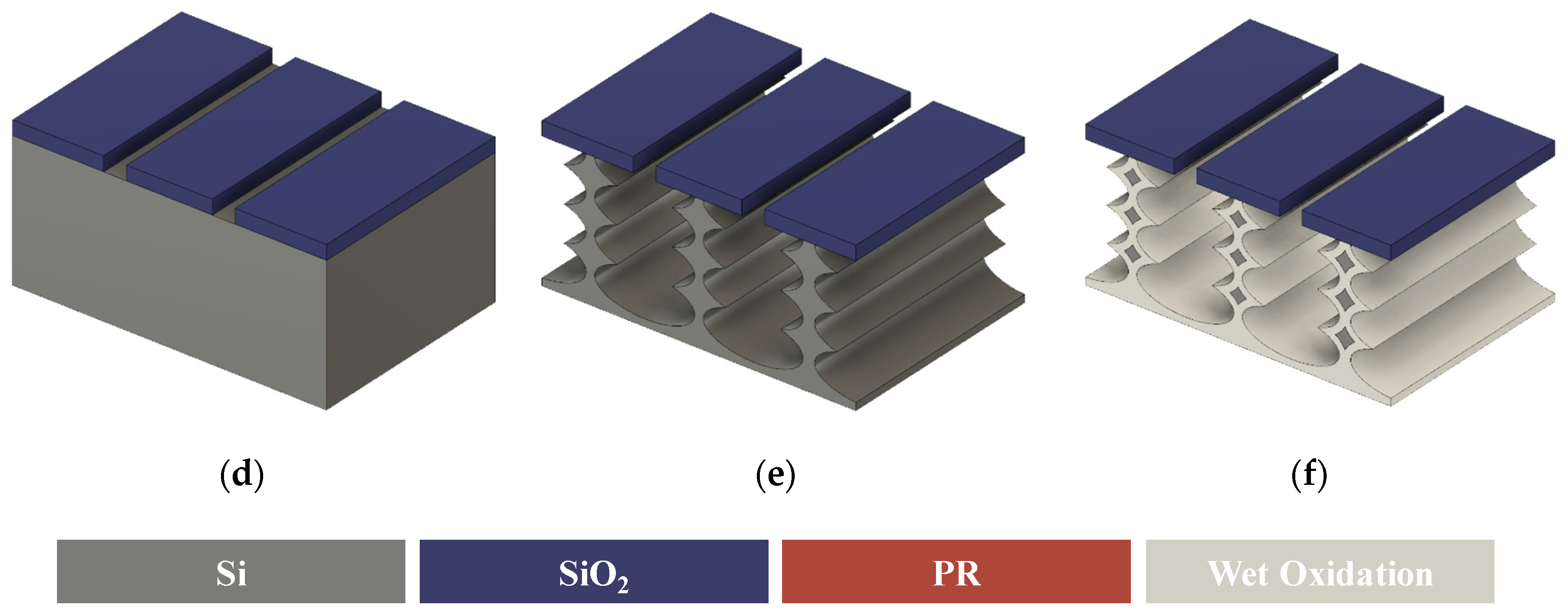
Based on this concept, the top-down fabrication proposed in this paper is depicted in
Figure 2. As previously mentioned, it uses a combination of photolithography, DRIE, and a wet-oxidation process. Moreover, a p-type (111)-oriented single-crystalline silicon wafer is used, which has a diameter of 100 mm, a thickness of 525 μm, and a resistivity of 1–10 Ω∙cm. The reason for using (111)-silicon instead of the commonly used (100)-silicon is to allow the current to flow through the silicon nanowires rather than the bulk silicon part. In fact, (100)-silicon can also be used to fabricate laterally-aligned silicon-nanowire arrays, as our group has also reported in previous publication [
5]. However, in the case of (100)-silicon, only a single layer can be manufactured due to the orientation of the {111} plane and the wet etching characteristics of the silicon. In this paper, we need to implement a multiple layer-stacked array of silicon nanowires and isolate them from the silicon bulk. The (111) silicon is suitable for isolating the nanowire from the substrate because the silicon is rapidly etched sideways during wet etching [
6]. This facilitates the isolation of multilayered-nanowire array structures from the silicon bulk. First, as shown in
Figure 2a, an oxide-mask layer (3000 Å thick) is deposited by a plasma-enhanced chemical vapor deposition (PECVD) process, with a radio frequency (RF) power of 350 W, an O
2 flow rate of 150 sccm, and a tetraethyl-orthosilicate (TEOS) flow rate of 150 sccm. The TEOS layer is used as a passivation hard mask for bulk silicon etching. A GRX-601 (AZ Electronic Materials, Luxembourg) photoresist (PR) film is spin-coated on the TEOS layer with a rotation speed of 4000 rpm and exposed to a UV light source with a wavelength of 365 nm for 3.1 s. Following the exposure, the PR is developed in an AZ 300 MIF developer for 18 s and then rinsed in deionized (DI) water, as shown in
Figure 2b. The photolithography step defines the in-plane dimension of the silicon-nanowire arrays, such as the pattern width and length.
After PR patterning, the TEOS hard-mask layer is etched by an inductive-coupled plasma (ICP) etcher with a CHF
3 flow rate of 25 sccm, a CF
4 flow rate of 5 sccm, and a pressure of 130 mTorr with an RF power of 600 W, as depicted in
Figure 2c. The target etching thickness of the TEOS layer is calculated to be approximately 110% of the deposited thickness, which guarantees the exposure of the silicon surface. As shown in
Figure 2d, after the PR strip step, a piranha solution (a mixture of sulfuric acid and hydrogen peroxide) cleaning process and an O
2 plasma ashing process are conducted to remove the residuals. In
Figure 2e, the bulk silicon is etched using a cyclic DRIE process, which consists of a single deposition step and two etching steps. In a conventional Bosch process, polymer deposition, polymer etching, and isotropic-silicon etching are conducted for five seconds, three seconds, and five seconds, respectively, in order to configure a high aspect-ratio structure. However, the process developed in this paper controls the final silicon etching time to fabricate the protrusion structures, which are in a location where the silicon nanowires are formed. The detailed DRIE process is summarized in
Table 1. Several experiments are performed to optimize the adequate scallop size by tuning the duration of the isotropic-silicon etching step.
As shown in
Figure 2f, a thermal wet-oxidation process is conducted to define the width and thickness of the silicon nanowire, both of which can be precisely controlled according to the wet- oxidation time. The process is performed under a temperature of 1000 °C with an H
2 flow rate of 7000 sccm and an O
2 flow rate of 6500 sccm. In essence, the wet-oxidation process consumes silicon to produce thermal oxide; hence, the silicon nanowires are fabricated under a protrusion structure, while the vertical layers are isolated by the insulation layers. In this paper, Bosch 5/3/15 process is used for DRIE, and the purpose is to fabricate nanowires with a width of approximately 300 nm. The wet oxidation rate of the furnace used in this process is approximately 50 Å/min to form nanostructures, and the oxidation process is performed for about 70 min to isolate each layer by completely oxidizing the support structure. The additional oxidation is 20–25% more than the width of the support structure because the rate of oxidation is slower than the surface.
After removing the TEOS and thermal oxide layers by hydrofluoric (HF)-acid dipping, the vertically-stacked silicon-nanowire arrays are formed. The number of vertical layers can be adjusted by the number of DRIE-process cycles without additional masking or photolithography processes.
3. Fabrication Results
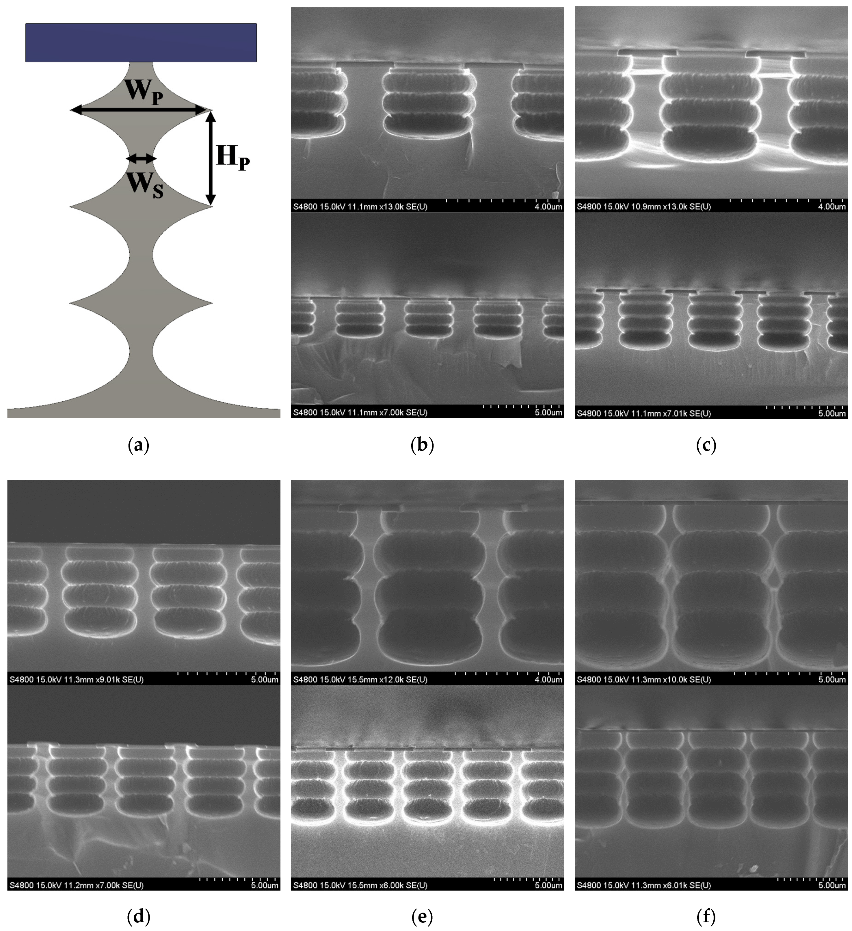
For the fabrication of vertically-stacked silicon-nanowire arrays, it is necessary to define a structure with protrusion and support, as shown in
Figure 3. Indeed, the difference between the protrusion and support widths determines the wet-oxidation process time, which, in turn, determines the dimensions of the silicon nanowires fabricated in the protrusion. In addition, if the width of the support is too narrow, or if the support does not form, then the thermal oxide layer will not grow uniformly during the wet-oxidation process. Therefore, the most critical step of the proposed fabrication method is the DRIE process, especially the isotropic-silicon etching step, which determines the scallop size.
The experimental results of the DRIE process with the tuning of the isotropic-silicon etching time are shown in
Figure 4 and summarized in
Table 2. By adjusting the duration of the silicon etching, the size and depth of the scallop can be adjusted. A deep and wide scallop size can be obtained by a long silicon etching time. To find the optimal process conditions, the duration of the silicon-etching step is divided into five conditions: 5, 7, 10, 15, and 18 s. After the DRIE process, cross-sectional SEM imaging is performed to measure the protrusion width (
WP), vertical gap between protrusions (
HP) and the support width (
WS) for the isotropic silicon etching results. As a result, the etch rates for
WP,
HP and
WS are measured to be 0.04, 0.12, and 0.07 μm/s, respectively. Among the five process conditions, a suitable condition for the difference in width between the protrusion and the support is determined through experimentation. Indeed, a silicon-etching time of 15 s produces an adequate scallop size for the fabrication of the vertically-stacked silicon nanowires.
In
Figure 5, the fabrication results of the vertically-stacked silicon-nanowire arrays are presented. As is well known, for oxidation with lower oxide thickness, the rate of oxide growth is much faster than that predicted by the Deal–Grove model [
24]. However, in the case of oxidation of a certain thickness, there is a region with almost linear characteristics. In this paper, the conditions that can grow 500 nm oxide for the fabrication of silicon nanowires having a width of approximately 300 nm are conducted with a process time between 60 and 90 min. Of course, when the oxidation thickness becomes thick, and thus the oxidation process takes a long time, non-linear characteristics are exhibited as the silicon consumed decreases. Therefore, if possible, the width of the pattern should be reduced during the initial UV lithography process, and a suitable scallop size should be produced to form silicon nanowires of the desired thickness. In the process developed in this study, the UV lithography and the PR films form a pattern width that is narrower than the line width of the mask. In addition, with the repeated experiments, the process secures its reproducibility. In
Figure 5a,b, the fabrication results after the optimum wet-oxidation and excessive wet-oxidation are shown, respectively. As can be seen in
Figure 5a,b, an appropriate width difference between the protrusion and the support is vital with respect to forming a silicon nanowire with uniform dimensions. In addition, the wet-oxidation process time is recommended to proceed for the minimum time required for layer-to-layer isolation. In case of excessive wet oxidation, narrow silicon nanowires can form; however, deviations in the dimensions increase accordingly.
Figure 6 shows the silicon-nanowire structures released after completion of the wet oxidation process. As shown in
Figure 6a, after wet oxidation, the supporting part is completely oxidized and removed by HF-acid dipping, indicating that each silicon nanowire is formed individually. In
Figure 6b, it can be seen that an array of silicon nanowires having a length of approximately 20 μm is formed, and a silicon-nanowire array consisting of three vertically-stacked layers can be seen from the cross-sectional SEM image. However, after the release of the silicon nanowires, it is difficult to verify the uniformity of the cross-sectional width, and the cross-sectional width can only be confirmed by SEM imaging after wet oxidation.
4. Discussion and Conclusions
In this paper, a novel top-down method for fabricating vertically-stacked silicon-nanowire arrays was presented. This method enables the fabrication of lateral silicon-nanowire arrays in a vertical direction, as well as the fabrication of an increased number of silicon nanowires on a finite dimension, which, in turn, results in increased sensitivity and a dynamic range. This paper also deals with the considerations in each process when manufacturing nanowires with different dimensions. The proposed fabrication process used single UV lithography, DRIE, and wet-oxidation processes. First, the patterns of the silicon-nanowire array were defined by photolithography. However, the UV lithography has limited resolution, so the number of silicon nanowires that can be fabricated per unit area is limited. The silicon-nanowire arrays in this paper were fabricated at the wafer-level and used as one building block for the purpose of integration with other electronic devices. Therefore, this paper dealt with a process method of increasing the number of silicon nanowires per unit area by vertically stacking to improve the sensing characteristics. Then, the structures in which the silicon nanowires form were defined by DRIE, where the number of vertically-stacked arrays can be adjusted by the number of dry-etching repetitions. Finally, the silicon nanowires were formed through a wet-oxidation process, where the silicon-nanowire dimensions can be precisely controlled by the process time. The uniformity of the silicon nanowires created on each layer is, in turn, most affected by the uniformity of the scallop with the depth of the DRIE process. Through various experiments in this paper, the process conditions in which the scallop can be produced most uniformly according to depth were derived, and the size of the protrusion and support produced when it was done in accordance with this condition were measured and evaluated. Depending on the oxidation process time, the dimension of the silicon nanowires is also affected. To this end, we measured the width of the protrusion and support and conducted the oxidation process only for the optimal time for isolating the layer.
Figure 5 discusses the possible imbalance when the oxidation process is carried out for the optimum time and excessive time.
Using the proposed method, the fabrication results of the vertically-stacked silicon-nanowire array consisting of three vertical layers are shown. It is expected that the amount of current output from the sensor can be increased when implementing chemical or optical sensors using it. Each layer is equipped with twenty well-aligned diamond-shaped silicon nanowires with the dimensions of a single nanowire of approximately 300 nm in width and 20 μm in length. Indeed, this should lead to highly sensitive, reproducible, and low-cost silicon-nanowire sensors that can be used for a number of applications. In this paper, we created a three-layered silicon-nanowire array, but using this process, it is possible to produce more than three layers. The latest DRIE equipment is capable of deep silicon etching with a scale of up to tens of um uniform size scallops, and the depth of the silicon-nanowire array on the third floor produced in this paper is approximately 5 μm. Therefore, the proposed method is expected to fabricate silicon-nanowire arrays with a more vertically-stacked structure. In addition, the proposed method can reduce the process complexity and facilitate monolithic integration when combining silicon nanowire-based sensors and CMOS circuits.


