Building Reliable Massive Capacity SSDs through a Flash Aware RAID-Like Protection †


Abstract
1. Introduction
2. Background and Related Work
2.1. Basics of Flash Memory and SSDs
2.2. Write Amplification in Flash Memory
2.3. Reliability of Flash Memory
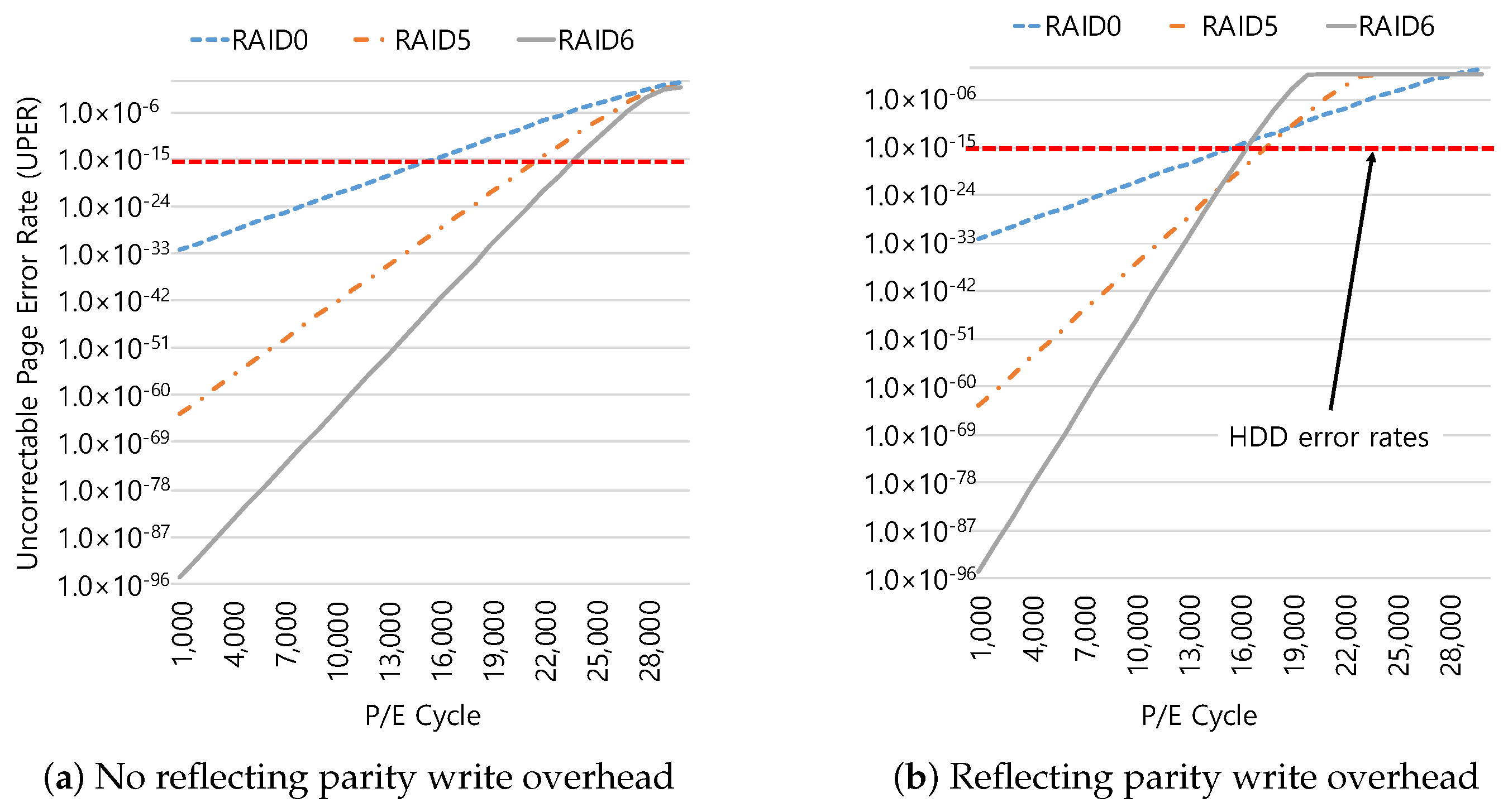
3. Motivation
- (1)
- We first obtain the P/E cycles from the SSD simulator for Financial workload.
- (2)
- (3)
- (4)
- (5)
- Because RAID6 maintains two parities per stripe, the error rate can be further reduced and it is calculated by Equation (5).
4. Design of mSAPL
4.1. Design Goal and Approach
- It is necessary to cope with more than one failure per stripe due to employing a large number of flash memories in a massive capacity SSD.
- In order to minimize the overhead caused by parity management, a parity update policy should be designed in order to minimize a GC overhead in SSDs.
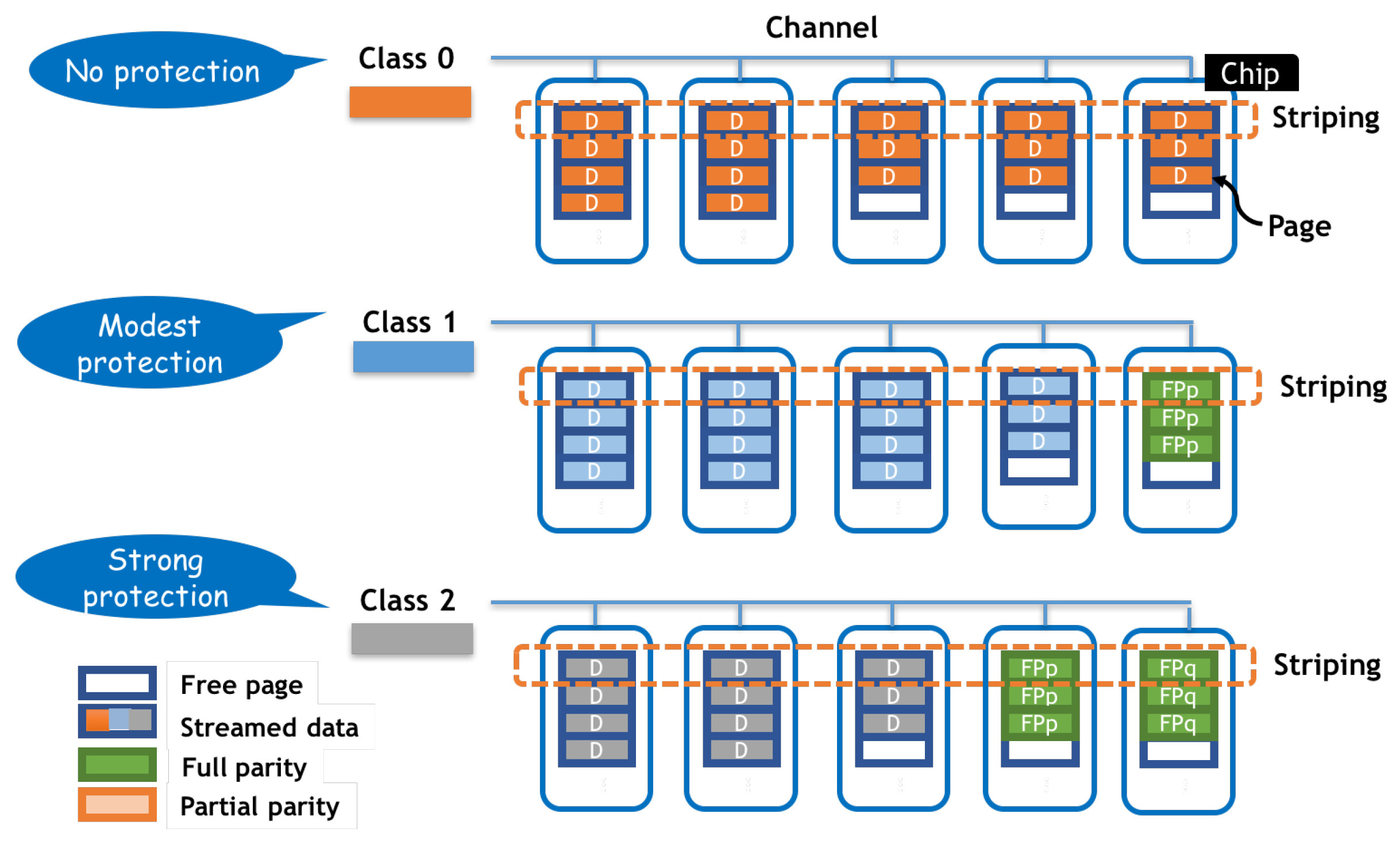
- Applying the same protection strength to all data in a massive flash based storage is not suitable for both performance and reliability aspects. Different protection strengths are needed for different kinds of data type or a user specification among massive volume of data.
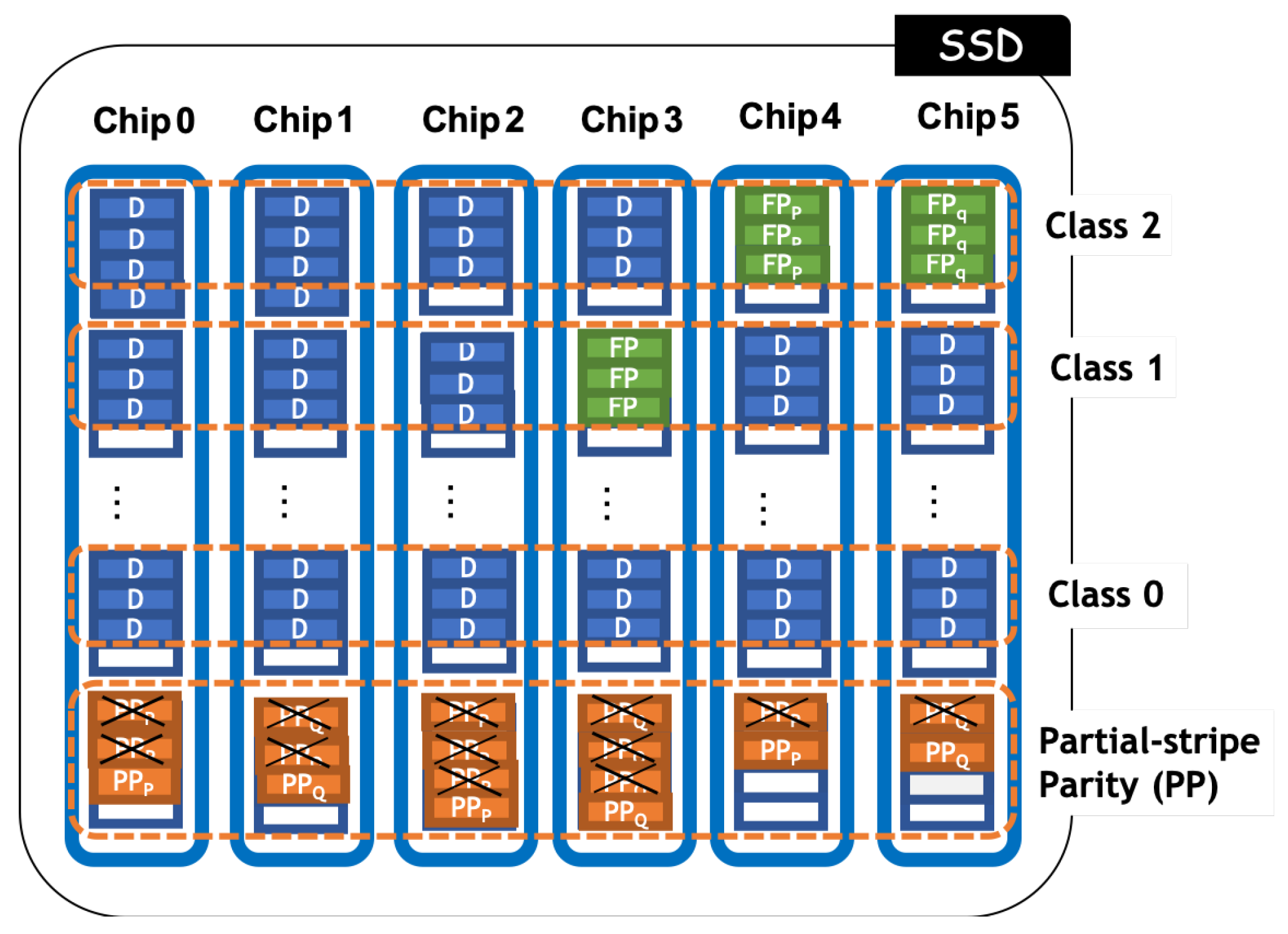
4.2. Differentiate Protection Strength through Classification
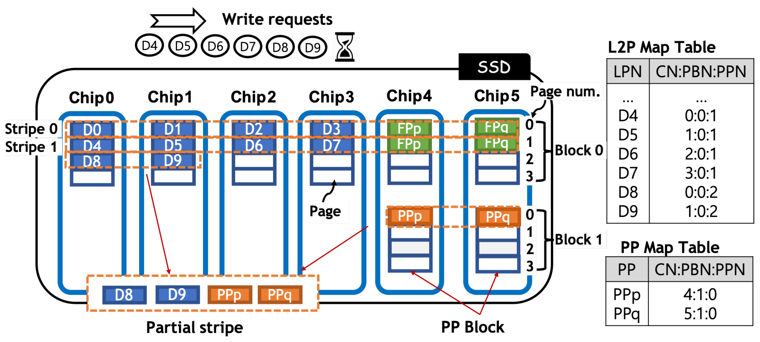
4.3. Data Placement in a Stripe
4.4. Partial-Stripe Parity Space of mSAPL
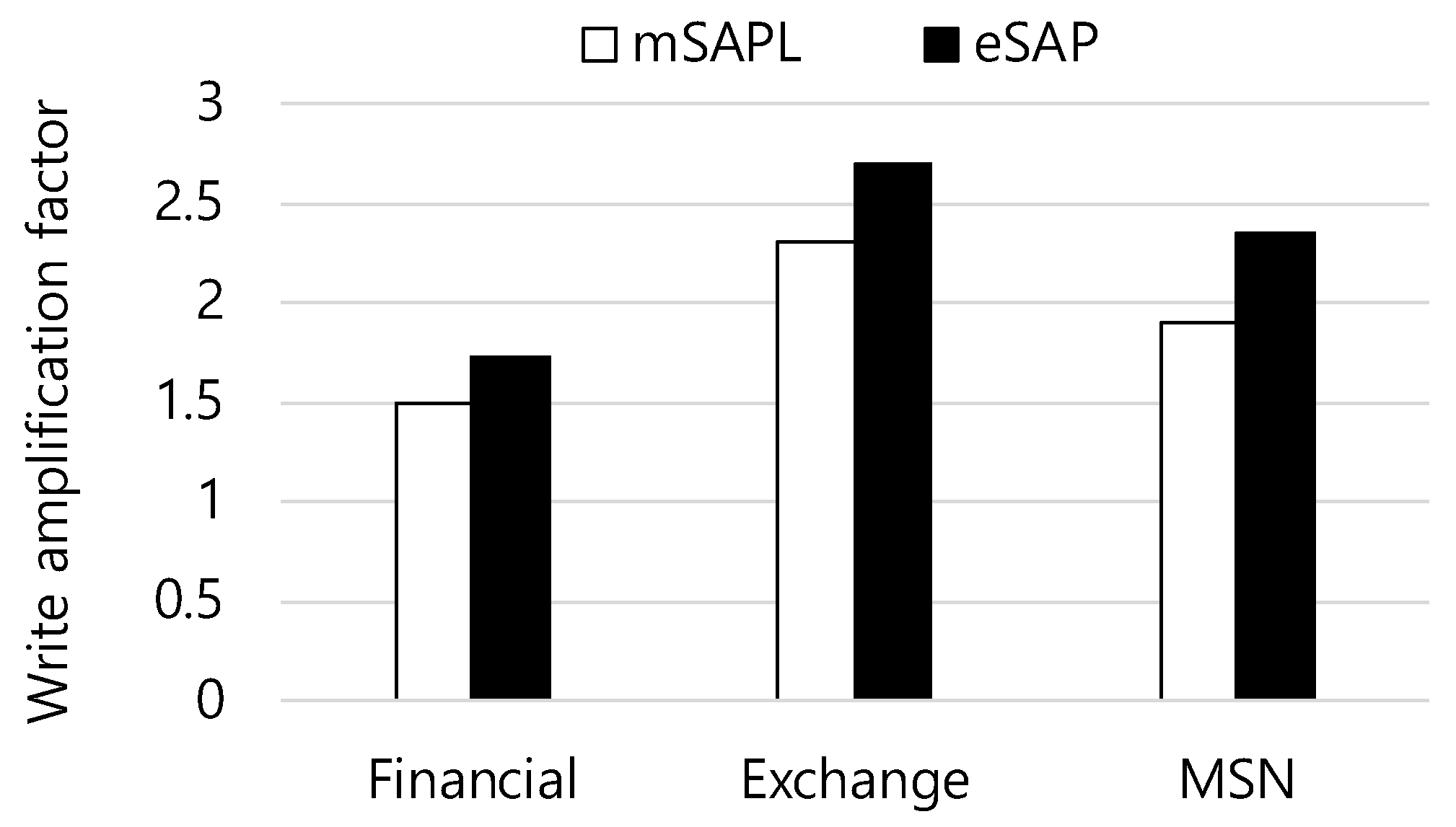
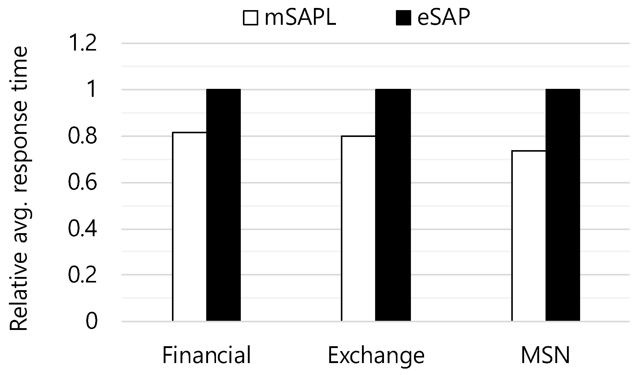
5. Performance Evaluation
5.1. Write Amplification Factor
5.2. Response Time
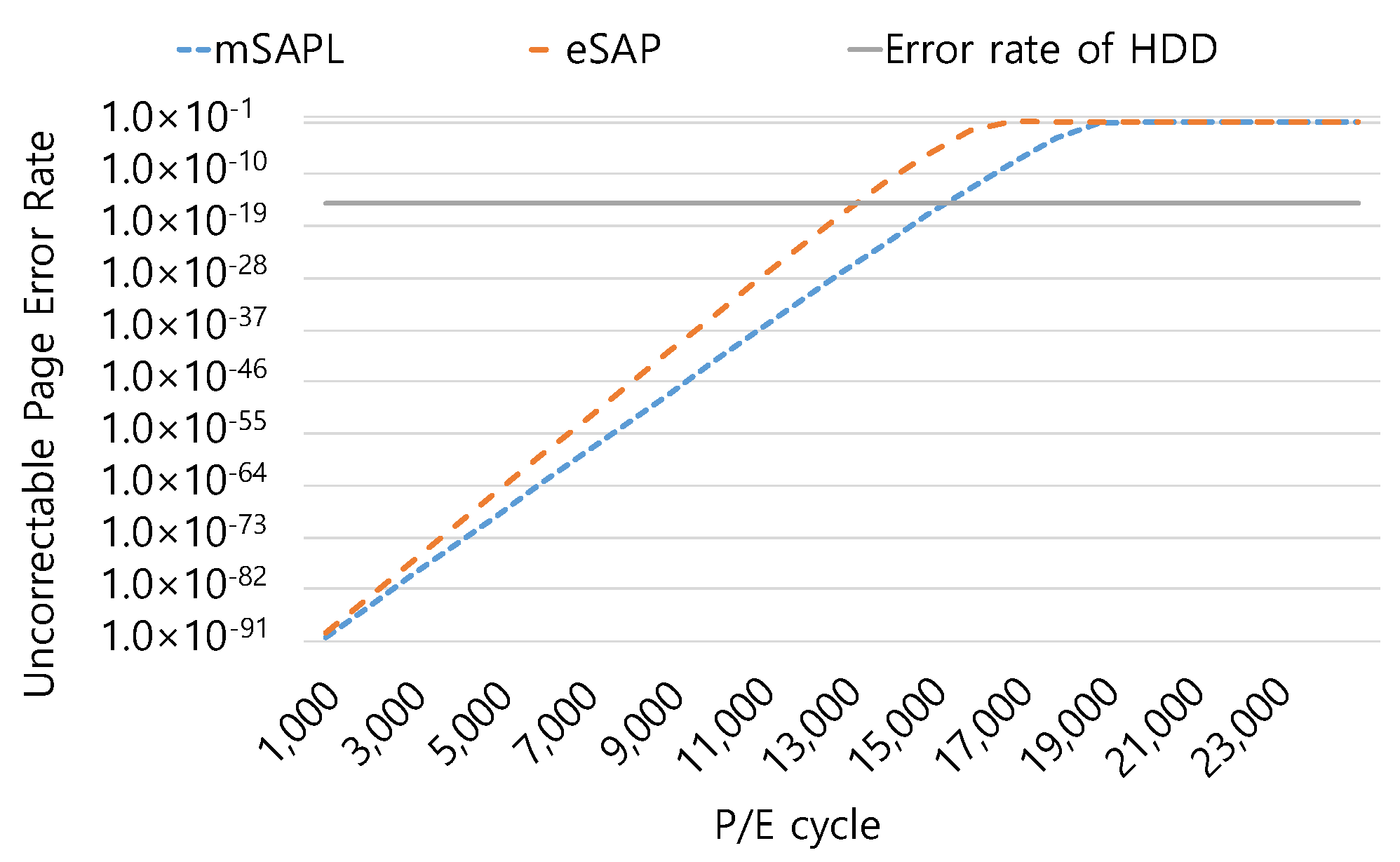
6. Analysis of Reliability and Lifetime of SSDs
7. Conclusions
Author Contributions
Funding
Conflicts of Interest
References
- Siddiqa, A.; Karim, A.; Gani, A. Big data storage technologies: A survey. Front. Inf. Technol. Electron. Eng. 2017, 18, 1040–1070. [Google Scholar] [CrossRef]
- Wikipedia. Flash Memory. 2019. Available online: https://en.wikipedia.org/wiki/Flash_memory (accessed on 20 November 2020).
- Samsung. Enterprise SSDs. 2019. Available online: http://www.samsung.com/semiconductor/ssd/enterprise-ssd/ (accessed on 20 November 2020).
- Kingsley-Hughes, A. World’s lArgest SSD Hits 100TB. 2018. Available online: https://www.zdnet.com/article/worlds-largest-ssd-hits-100tb/ (accessed on 20 November 2020).
- Tung, L. ‘World’s Largest’ SSD Revealed as Seagate Unveils 60TB Monster. 2016. Available online: https://www.zdnet.com/article/worlds-largest-ssd-revealed-as-seagate-unveils-60tb-monster/ (accessed on 20 November 2020).
- Nimbus Data World’s Highest Capacity and Most Efficient SSDs. 2020. Available online: https://nimbusdata.com/products/exadrive/ (accessed on 20 November 2020).
- Samsung. Samsung Electronics Begins Mass Production of Industry’s Largest Capacity SSD-30.72TB-for Next-Generation Enterprise Systems. 2018. Available online: https://news.samsung.com/global/samsung-electronics-begins-mass-production-of-industrys-largest-capacity-ssd-30-72tb-for-next-generation-enterprise-systems (accessed on 20 November 2020).
- Mearian, L. Samsung’s Massive 15TB SSD Can Be Yours. 2016. Available online: https://www.computerworld.com/article/3101165/samsungs-massive-15tb-ssd-can-be-yours-for-about-10k.html (accessed on 20 November 2020).
- Moon, S.; Reddy, A.L.N. Don’t Let RAID Raid the Lifetime of Your SSD Array. In Proceedings of the 5th USENIX Conference on Hot Topics in Storage and File Systems, San Jose, CA, USA, 27–28 June 2013. [Google Scholar]
- Kim, J.; Lee, J.; Choi, J.; Lee, D.; Noh, S.H. Improving SSD Reliability with RAID via Elastic Striping and Anywhere Parity. In Proceedings of the 43rd Annual IEEE/IFIP International Conference on Dependable Systems and Networks (DSN), Budapest, Hungary, 24–27 June 2013. [Google Scholar]
- Im, S.; Shin, D. Flash-Aware RAID Techniques for Dependable and High-Performance Flash Memory SSD. IEEE Trans. Comput. 2011, 60, 80–92. [Google Scholar] [CrossRef]
- Lee, Y.; Jung, S.; Song, Y.H. FRA: A flash-aware redundancy array of flash storage devices. In Proceedings of the CODES+ISSS ’09, Grenoble, France, 11–16 October 2009; pp. 163–172. [Google Scholar]
- Micron. NAND Flash Media Management Through RAIN. 2011. Available online: https://www.micron.com/~/media/documents/products/technical-marketing-brief/brief-ssd-rain.pdf (accessed on 20 November 2020).
- Kim, J.; Lee, E.; Choi, J.; Lee, D.; Noh, S.H. Chip-Level RAID with Flexible Stripe Size and Parity Placement for Enhanced SSD Reliability. IEEE Trans. Comput. 2016, 65, 1116–1130. [Google Scholar] [CrossRef]
- Wikipedia. Standard RAID Levels. 2019. Available online: https://en.wikipedia.org/wiki/Standard_RAID_levels (accessed on 20 November 2020).
- Mesnier, M.P.; Akers, J.B. Differentiated Storage Services. SIGOPS Oper. Syst. Rev. 2011, 45, 45–53. [Google Scholar] [CrossRef]
- Kim, J.; Lee, E.; Park, J.K. Flash based SSD Aware Parity Logging for Building Reliable Massive Capacity SSDs. In Proceedings of the 2020 IEEE International Conference on Consumer Electronics (ICCE), Las Vegas, NV, USA, 4–6 January 2020; pp. 1–4. [Google Scholar]
- Prabhakaran, V.; Wobber, T. SSD Extension for DiskSim Simulation Environment. 2008. Available online: http://research.microsoft.com/en-us/downloads/b41019e2-1d2b-44d8-b512-ba35ab814cd4 (accessed on 20 November 2020).
- Agrawal, N.; Prabhakaran, V.; Wobber, T.; Davis, J.D.; Manasse, M.; Panigrahy, R. Design tradeoffs for SSD performance. In 2008 USENIX ATC; USENIX Association: Berkeley, CA, USA, 2008; pp. 57–70. [Google Scholar]
- Seong, Y.J.; Nam, E.H.; Yoon, J.H.; Kim, H.; yong Choi, J.; Lee, S.; Bae, Y.H.; Lee, J.; Cho, Y.; Min, S.L. Hydra: A Block-Mapped Parallel Flash Memory Solid-State Disk Architecture. IEEE Trans. Comput. 2010, 59, 905–921. [Google Scholar] [CrossRef]
- Chen, F.; Koufaty, D.A.; Zhang, X. Understanding Intrinsic Characteristics and System Implications of Flash Memory Based Solid State Drives. In Proceedings of the Eleventh International Joint Conference on Measurement and Modeling of Computer Systems, Seattle, WA, USA, 15–19 June 2009; pp. 181–192. [Google Scholar]
- Jung, M.; Kandemir, M. An Evaluation of Different Page Allocation Strategies on High-speed SSDs. In Proceedings of the USENIX Workshop on Hot Topics in Storage and File Systems (HotStorage), Boston, MA, USA, 13–14 June 2012. [Google Scholar]
- Lee, J.; Byun, E.; Park, H.; Choi, J.; Lee, D.; Noh, S.H. CPS-SIM: Configurable and accurate clock precision solid state drive simulator. In Proceedings of the 2009 ACM Symposium on Applied Computing, Honolulu, HI, USA, 15–19 March 2009; pp. 318–325. [Google Scholar]
- Hu, Y.; Jiang, H.; Feng, D.; Tian, L.; Luo, H.; Zhang, S. Performance Impact and Interplay of SSD Parallelism Through Advanced Commands, Allocation Strategy and Data Granularity. In Proceedings of the International Conference on Supercomputing (ICS), Tucson, AZ, USA, 31 May–4 June 2011; pp. 96–107. [Google Scholar]
- Kim, J.; Kim, J.M.; Noh, S.; Min, S.L.; Cho, Y. A space-efficient flash translation layer for CompactFlash systems. IEEE Trans. Consum. Electron. 2002, 48, 366–375. [Google Scholar]
- Desnoyers, P. Analytic Models of SSD Write Performance. ACM Trans. Storage 2014, 10, 8:1–8:25. [Google Scholar] [CrossRef]
- Kwon, H.; Kim, E.; Choi, J.; Lee, D.; Noh, S.H. Janus-FTL: Finding the Optimal Point on the Spectrum between Page and Block Mapping Schemes. In Proceedings of the International Conference on Embedded Software (EMSOFT), Scottsdale, AZ, USA, 24–29 October 2010; pp. 169–178. [Google Scholar]
- Kim, B.S.; Choi, J.; Min, S.L. Design Tradeoffs for SSD Reliability. In Proceedings of the 17th USENIX Conference on File and Storage Technologies (FAST 19), Boston, MA, USA, 25–28 February 2019; pp. 281–294. [Google Scholar]
- Gunawi, H.S.; Suminto, R.O.; Sears, R.; Golliher, C.; Sundararaman, S.; Lin, X.; Emami, T.; Sheng, W.; Bidokhti, N.; McCaffrey, C.; et al. Fail-Slow at Scale: Evidence of Hardware Performance Faults in Large Production Systems. ACM Trans. Storage 2018, 14, 1–26. [Google Scholar] [CrossRef]
- Maneas, S.; Mahdaviani, K.; Emami, T.; Schroeder, B. A Study of SSD Reliability in Large Scale Enterprise Storage Deployments. In Proceedings of the 18th USENIX Conference on File and Storage Technologies (FAST 20), Santa Clara, CA, USA, 25–27 February 2020; pp. 137–149. [Google Scholar]
- Xu, E.; Zheng, M.; Qin, F.; Xu, Y.; Wu, J. Lessons and Actions: What We Learned from 10 K SSD-Related Storage System Failures. In Proceedings of the 2019 USENIX Conference on Usenix Annual Technical (ATC) Conference, Renton, WA, USA, 10–12 July 2019. [Google Scholar]
- Tai, A.; Kryczka, A.; Kanaujia, S.O.; Jamieson, K.; Freedman, M.J.; Cidon, A. Who’s Afraid of Uncorrectable Bit Errors? Online Recovery of Flash Errors with Distributed Redundancy. In Proceedings of the 2019 USENIX Conference on Usenix Annual Technical (ATC) Conference, Renton, WA, USA, 10–12 July 2019; pp. 977–991. [Google Scholar]
- Narayanan, I.; Wang, D.; Jeon, M.; Sharma, B.; Caulfield, L.; Sivasubramaniam, A.; Cutler, B.; Liu, J.; Khessib, B.; Vaid, K. SSD Failures in Datacenters: What? When? And Why? In Proceedings of the 9th ACM International on Systems and Storage Conference (SYSTOR), Haifa, Israel, 6–8 June 2016. [Google Scholar]
- Grupp, L.M.; Caulfield, A.M.; Coburn, J.; Swanson, S.; Yaakobi, E.; Siegel, P.H.; Wolf, J.K. Characterizing Flash Memory: Anomalies, Observations, and Applications. In Proceedings of the MICRO 42, New York, NY, USA, 12–16 December 2009. [Google Scholar]
- Grupp, L.M.; Davis, J.D.; Swanson, S. The Bleak Future of NAND Flash Memory. In Proceedings of the FAST’12; USENIX Association: San Jose, CA, USA, 2012; pp. 17–24. [Google Scholar]
- What Is QLC Flash and What Workloads It Is Good for? 2019. Available online: https://www.computerweekly.com/feature/What-is-QLC-flash-and-what-workloads-it-is-good-for (accessed on 20 November 2020).
- Cai, Y.; Haratsch, E.F.; Mutlu, O.; Mai, K. Error Patterns in MLC NAND Flash Memory: Measurement, Characterization, and Analysis. In Proceedings of the Design, Automation and Test in Europe Conference and Exhibition (DATE), Dresden, Germany, 12–16 March 2012; pp. 521–526. [Google Scholar]
- Mielke, N.; Marquar, T.; Wu, N.; Kessenich, J.; Belgal, H.; Schares, E.; Trivedi, F.; Goodness, E.; Nevill, L. Bit Error Rate in NAND Flash Memories. In Proceedings of the IEEE International Reliability Physics Symposium, Phoenix, AZ, USA, 27 April–1 May 2008; pp. 9–19. [Google Scholar]
- Sun, H.; Grayson, P.; Wood, B. Quantifying Reliability of Solid-State Storage from Multiple Aspects. In Proceedings of the IEEE International Workshop on Storage Network Architecture and Parallel I/O (SNAPI ’11), Denver, CO, USA, 25 May 2011. [Google Scholar]
- Breen, P.; Griffin, T.; Papandreou, N.; Parnell, T.; Tressler, G. 3D NAND Assessment for Next Generation Flash Applications; Santa Clara, CA, USA, 9–11 August 2016. Available online: https://www.flashmemorysummit.com/English/Collaterals/Proceedings/2016/20160810_FM22_Tressler.pdf (accessed on 20 November 2020).
- Kim, H.; Ahn, S.; Shin, Y.G.; Lee, K.; Jung, E. Evolution of NAND Flash Memory: From 2D to 3D as a Storage Market Leader. In Proceedings of the 2017 IEEE International Memory Workshop (IMW), Monterey, CA, USA, 14–17 May 2017; pp. 1–4. [Google Scholar]
- Papandreou, N.; Pozidis, H.; Parnell, T.; Ioannou, N.; Pletka, R.; Tomic, S.; Breen, P.; Tressler, G.; Fry, A.; Fisher, T. Characterization and Analysis of Bit Errors in 3D TLC NAND Flash Memory. In Proceedings of the 2019 IEEE International Reliability Physics Symposium (IRPS), Monterey, CA, USA, 31 March–4 April 2019; pp. 1–6. [Google Scholar]
- Luo, Y.; Ghose, S.; Cai, Y.; Haratsch, E.F.; Mutlu, O. Improving 3D NAND Flash Memory Lifetime by Tolerating Early Retention Loss and Process Variation. In Proceedings of the 2018 ACM International Conference on Measurement and Modeling of Computer Systems, Irvine, CA, USA, 18–22 June 2018; pp. 1–48. [Google Scholar]
- Mizoguchi, K.; Takahashi, T.; Aritome, S.; Takeuchi, K. Data-Retention Characteristics Comparison of 2D and 3D TLC NAND Flash Memories. In Proceedings of the 2017 IEEE International Memory Workshop (IMW), Monterey, CA, USA, 14–17 May 2017; pp. 1–4. [Google Scholar]
- Chen, S. What Types of ECC Should Be Used on Flash Memory? 2007. Available online: http://www.spansion.com/Support/AppNotes/ (accessed on 20 November 2020).
- Sommer, N. Signal Processing and the Evolution of NAND Flash Memory. 2010. Available online: https://www.embedded-computing.com/embedded-computing-design/signal-processing-and-the-evolution-of-nand-flash-memory (accessed on 20 November 2020).
- Deal, E. Trends in NAND Flash Memory Error Correction. Cyclic Design, White Paper. June 2009. Available online: http://www.cyclicdesign.com/whitepapers/Cyclic_Design_NAND_ECC.pdf (accessed on 1 October 2020).
- Mariano, M. ECC Options for Improving NAND Flash Memory Reliability. Micron. 2012. Available online: http://www.micron.com/support/software/~/media/Documents/Products/Software%20Article/SWNL_implementing_ecc.ashx (accessed on 20 November 2020).
- Lee, H.; Jung, S.; Song, Y.H. PCRAM-assisted ECC management for enhanced data reliability in flash storage systems. IEEE Trans. Consum. Electron. 2012, 58, 849–856. [Google Scholar] [CrossRef]
- Hu, Y.; Xiao, N.; Liu, X. An elastic error correction code technique for NAND flash-based consumer electronic devices. IEEE Trans. Consum. Electron. 2013, 59, 1–8. [Google Scholar] [CrossRef]
- Lee, S.; Lee, B.; Koh, K.; Bahn, H. A Lifespan-Aware Reliability Scheme for RAID-based Flash Storage. In Proceedings of the SAC’11, TaiChung, Taiwan, 21–24 March 2011; pp. 374–379. [Google Scholar]
- Zambelli, C.; Marelli, A.; Micheloni, R.; Olivo, P. Modeling the Endurance Reliability of Intradisk RAID Solutions for Mid-1X TLC NAND Flash Solid-State Drives. IEEE Trans. Device Mater. Reliab. 2017, 17, 713–721. [Google Scholar] [CrossRef]
- Park, H.; Kim, J.; Choi, J.; Lee, D.; Noh, S.H. Incremental redundancy to reduce data retention errors in flash-based SSDs. In Proceedings of the 2015 31st Symposium on Mass Storage Systems and Technologies (MSST), Santa Clara, CA, USA, 30 May–5 June 2015; pp. 1–13. [Google Scholar]
- Pan, W.; Xie, T. A Mirroring-Assisted Channel-RAID5 SSD for Mobile Applications. ACM Trans. Embed. Comput. Syst. 2018, 17, 1–27. [Google Scholar] [CrossRef]
- Gary, J.; van Ingen, C. Empirical Measurements of Disk Failure Rates and Error Rates; Technical Report MSR-TR-2005-166; Microsoft: Redmond, WA, USA, December 2005. [Google Scholar]
- Thereska, E.; Ballani, H.; O’Shea, G.; Karagiannis, T.; Rowstron, A.; Talpey, T.; Black, R.; Zhu, T. IOFlow: A Software-defined Storage Architecture. In Proceedings of the ACM Symposium on Operating Systems Principles (SOSP), Farmington, PA USA, 3–6 November 2013; pp. 182–196. [Google Scholar]
- Kang, J.U.; Hyun, J.; Maeng, H.; Cho, S. The Multi-streamed Solid-State Drive. In Proceedings of the USENIX Workshop on Hot Topics in Storage and File Systems (HotStorage), Philadelphia, PA, USA, 17–18 June 2014. [Google Scholar]
- JEDEC. Data Tag Mechanism of eMMC. “Standard Specification No. JESD84-B45”. Available online: http://www.jedec.org/sites/default/files/docs/jesd84-B45.pdf (accessed on 20 November 2020).
- Gupta, A.; Kim, Y.; Urgaonkar, B. DFTL: A flash translation layer employing demand-based selective caching of page-level address mappings. In Proceedings of the 14th International Conference on Architectural Support for Programming Languages and Operating Systems, Washington, DC, USA, 7–11 March 2009; pp. 229–240. [Google Scholar]
- Rho, E.; Joshi, K.; Shin, S.U.; Shetty, N.J.; Hwang, J.; Cho, S.; Lee, D.D.; Jeong, J. FStream: Managing Flash Streams in the File System. In Proceedings of the 16th USENIX Conference on File and Storage Technologies (FAST 18), Renton, WA, USA, 9–11 April 2018; USENIX Association: Oakland, CA, USA, 2018; pp. 257–264. [Google Scholar]


| Parameter | Value | Parameter | Value |
|---|---|---|---|
| Total capacity | 128 GB | No. of chips | 8 |
| Planes per chip | 8 | Blocks per plane | 2048 |
| Pages per block | 128 | Page size | 8 KB |
| Over-provisioning | 4% | GC policy | Greedy |
| Write time | 800 us | Read time | 60 us |
| Erase time | 1.5 ms | Page Xfer time | 30 ns |
| Parities per stripe | 2 | Stripe size | 8 × 4 KB |
| Workload | Request | Write | Average |
|---|---|---|---|
| Total | Ratio | Req. Size | |
| Financial | 14.1 GB | 0.76 | 14 KB |
| MSN | 28.2 GB | 0.96 | 27 KB |
| Exchange | 19.2 GB | 0.67 | 17 KB |
Publisher’s Note: MDPI stays neutral with regard to jurisdictional claims in published maps and institutional affiliations. |
© 2020 by the authors. Licensee MDPI, Basel, Switzerland. This article is an open access article distributed under the terms and conditions of the Creative Commons Attribution (CC BY) license (http://creativecommons.org/licenses/by/4.0/).
Share and Cite
Kim, J.; Park, J.K. Building Reliable Massive Capacity SSDs through a Flash Aware RAID-Like Protection. Appl. Sci. 2020, 10, 9149. https://doi.org/10.3390/app10249149
Kim J, Park JK. Building Reliable Massive Capacity SSDs through a Flash Aware RAID-Like Protection. Applied Sciences. 2020; 10(24):9149. https://doi.org/10.3390/app10249149
Chicago/Turabian StyleKim, Jaeho, and Jung Kyu Park. 2020. "Building Reliable Massive Capacity SSDs through a Flash Aware RAID-Like Protection" Applied Sciences 10, no. 24: 9149. https://doi.org/10.3390/app10249149
APA StyleKim, J., & Park, J. K. (2020). Building Reliable Massive Capacity SSDs through a Flash Aware RAID-Like Protection. Applied Sciences, 10(24), 9149. https://doi.org/10.3390/app10249149