Article

Design of Heterogenous Two-Element Array Antenna on an Electrically Thick Substrate for High Isolation and Low Pattern Correlation Using Modal Difference in Radiation Patterns

1
School of Electronic and Electrical Engineering, Hongik University, Seoul 04066, Korea
2
School of Electronic and Electrical Engineering, Kookmin University, Seoul 02703, Korea
*
Author to whom correspondence should be addressed.
Appl. Sci. 2020, 10(11), 3916; https://doi.org/10.3390/app10113916
Submission received: 27 April 2020 / Revised: 1 June 2020 / Accepted: 4 June 2020 / Published: 5 June 2020

Abstract

:
In this paper, we propose a novel design of a two-element array antenna on an electrical thick substrate with an extremely narrow array distance. The proposed array consists of a rectangular ring patch printed on a thick substrate and a monopole wire in the center of the substrate. Each element has a modal difference in the radiation pattern, causing high isolation and low correlation between the array elements. From the measurement results, the monopole and patch elements exhibit reflection coefficients of −10 dB and −10.7 dB with peak gains of 3.8 dBi and 6.1 dBi, respectively, at 1.6 GHz. The mutual coupling between the two elements is −20.7 dB. For modal analysis of the antenna pattern, spherical mode decomposition is performed on the radiation patterns of the two elements, and low envelope correlation coefficient levels below 16% are maintained. We also investigate the antijamming performance using a power inversion algorithm in a practical pattern nulling application; a null depth of −47.7 dB and a null width of 33.2° are obtained when the interference signal arrives at the elevation angle of 45°.

1. Introduction

Recent dramatic developments in wireless communications have resulted in an environment where many signals from various communication systems, such as 4G, 5G, Wi-Fi, Bluetooth, global positioning system (GPS), and Zigbee, exist simultaneously in a limited space [1,2,3,4,5,6,7]. Such signals from the antennas of various wireless devices can cause significant signal interference internally and externally. To mitigate interference, pattern nulling and forming techniques have been extensively studied and used in practical applications with array antennas by adjusting the weight of each antenna element [8,9,10,11,12,13,14,15,16]. However, the pattern nulling performance is significantly degraded when multiple antennas in the array are placed in a limited platform size. This nulling performance degradation is caused in part by increased mutual coupling of the array, where the distance between adjacent elements is too close. The spatial diversity of the array antenna is also reduced, since the radiation patterns of individual elements have a high pattern correlation, resulting in inferior pattern nulling or forming performance. To overcome these drawbacks, many studies have been carried out to minimize the mutual couplings and pattern correlations for compact array antennas, which include using parasitic elements [17,18,19], defected or extended ground planes [20,21,22], electromagnetic band-gap structures [23,24,25], and ferrite materials [26,27,28]. Although these previous studies can improve the isolation and maintain the low pattern correlations between adjacent array elements, these techniques are sometimes not feasible in small devices with limited spaces. Thus, research on mounting the array antennas in such compact spaces has been conducted by incorporating multiple radiating modes of each array element [29,30,31] or employing dissimilar antenna types such as a patch antenna with a monopole antenna [32,33,34,35] and a patch type antenna with a dielectric resonating antenna [36,37]. Furthermore, there is a study on using different antenna types (a circular patch antenna and a cylindrical monopole antenna) to operate in the higher order mode at multiband frequencies [38,39]. However, in these studies, the electrical antenna size is still large because it is necessary to achieve higher order modes. In addition, it is difficult to control the mutual coupling and the pattern correlation due to the shape of the patch antenna when the array elements are close to each other with sharing a common ground [40,41].
In this paper, we propose a novel design of a two-element array antenna on an electrically thick substrate with an extremely narrow array distance, where each element has a modal difference in the radiation pattern, causing a high isolation and a low correlation between the array elements. The proposed array consists of a rectangular ring patch printed on a thick substrate and a monopole wire in the center of the substrate. These two types of antennas share the ground plate, and the antenna ports are very close to each other while minimizing distortion in antenna performances. To demonstrate the feasibility of the proposed structure, the antenna is fabricated to measure the characteristics of the reflection coefficients, mutual couplings, and radiation patterns. For modal analysis of the antenna pattern, spherical mode decomposition is performed on the radiation patterns of the two elements to ensure that each antenna pattern has a significant modal difference with respect to spherical modes. Then, we define a modal difference metric (MDM) to indicate a quantitative value of the modal difference for the two-array elements. In addition, the envelope correlation coefficients (ECCs) of the proposed array in terms of the interelement spacing are observed and compared to the conventional patch and monopole arrays. Finally, to verify the proposed array in a practical pattern nulling application, we investigate the antijamming or anti-interference performance using a conventional power inversion (PI) algorithm. The jamming signal is modeled by a chirp signal with a specific bandwidth, and white Gaussian noise is added to model a typical communication environment. Then, the receiving jamming signal is mitigated by changing the weights of the array elements using the PI algorithm. Nulling performances such as the null direction of angle (DOA) errors, null depth, and null width for the proposed array are compared to the conventional patch and monopole arrays. The results demonstrate that the proposed array antenna can provide high nulling performance, while having an extremely narrow interelement spacing.

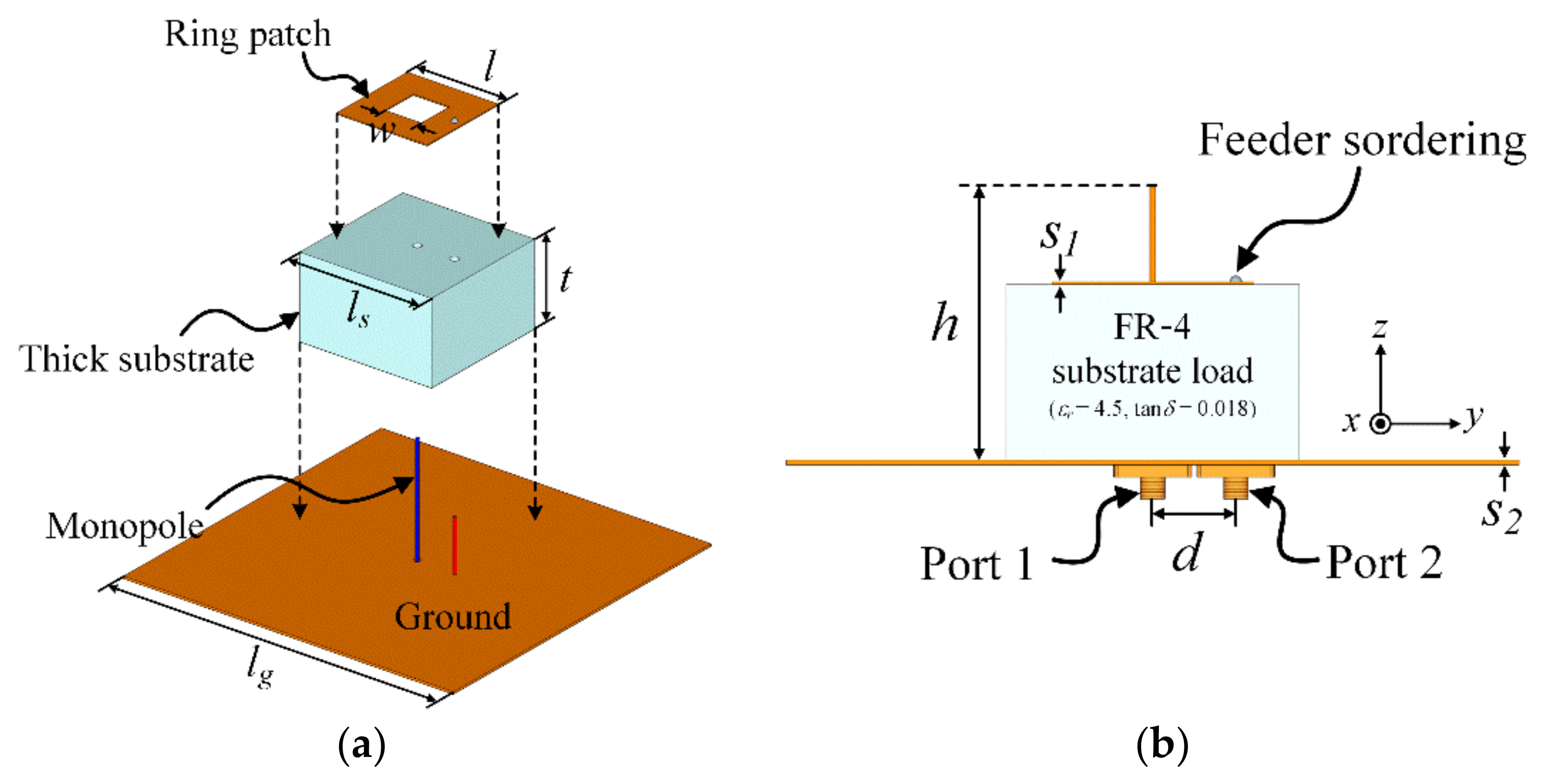
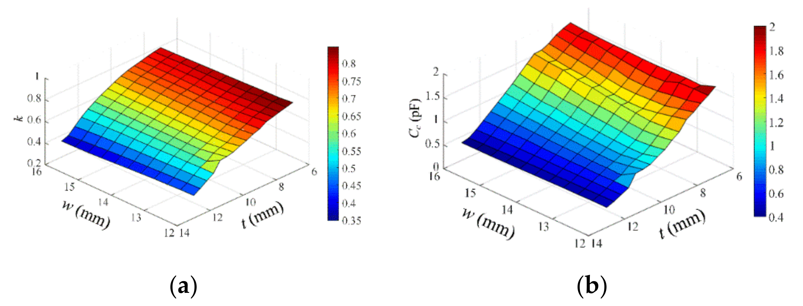
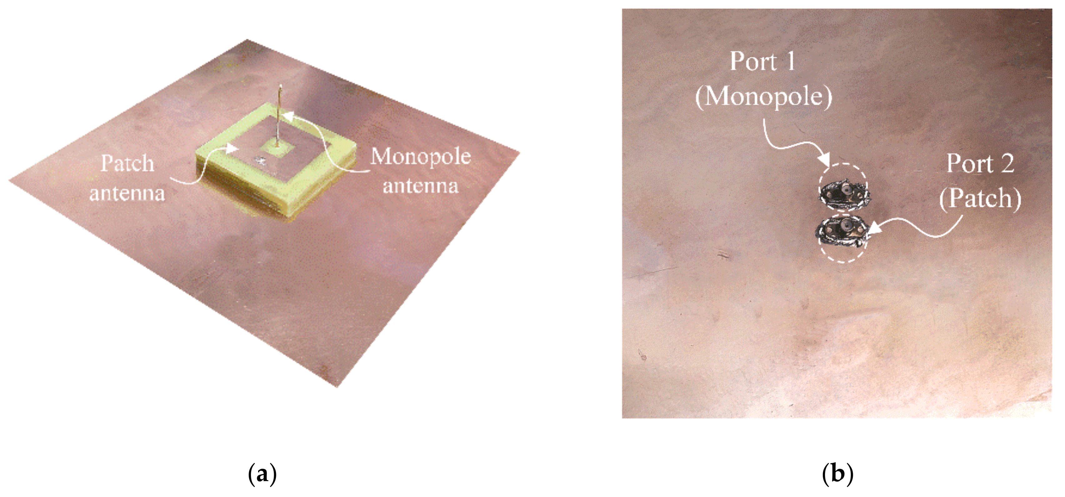
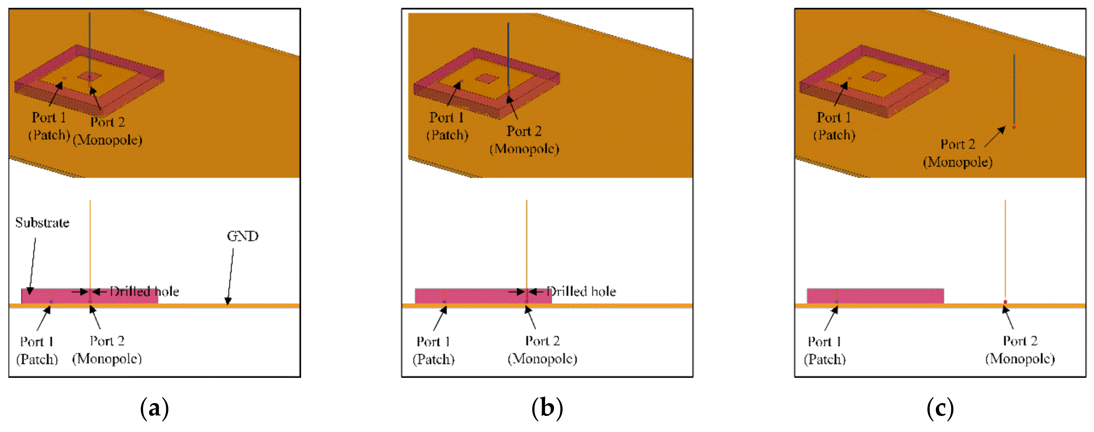
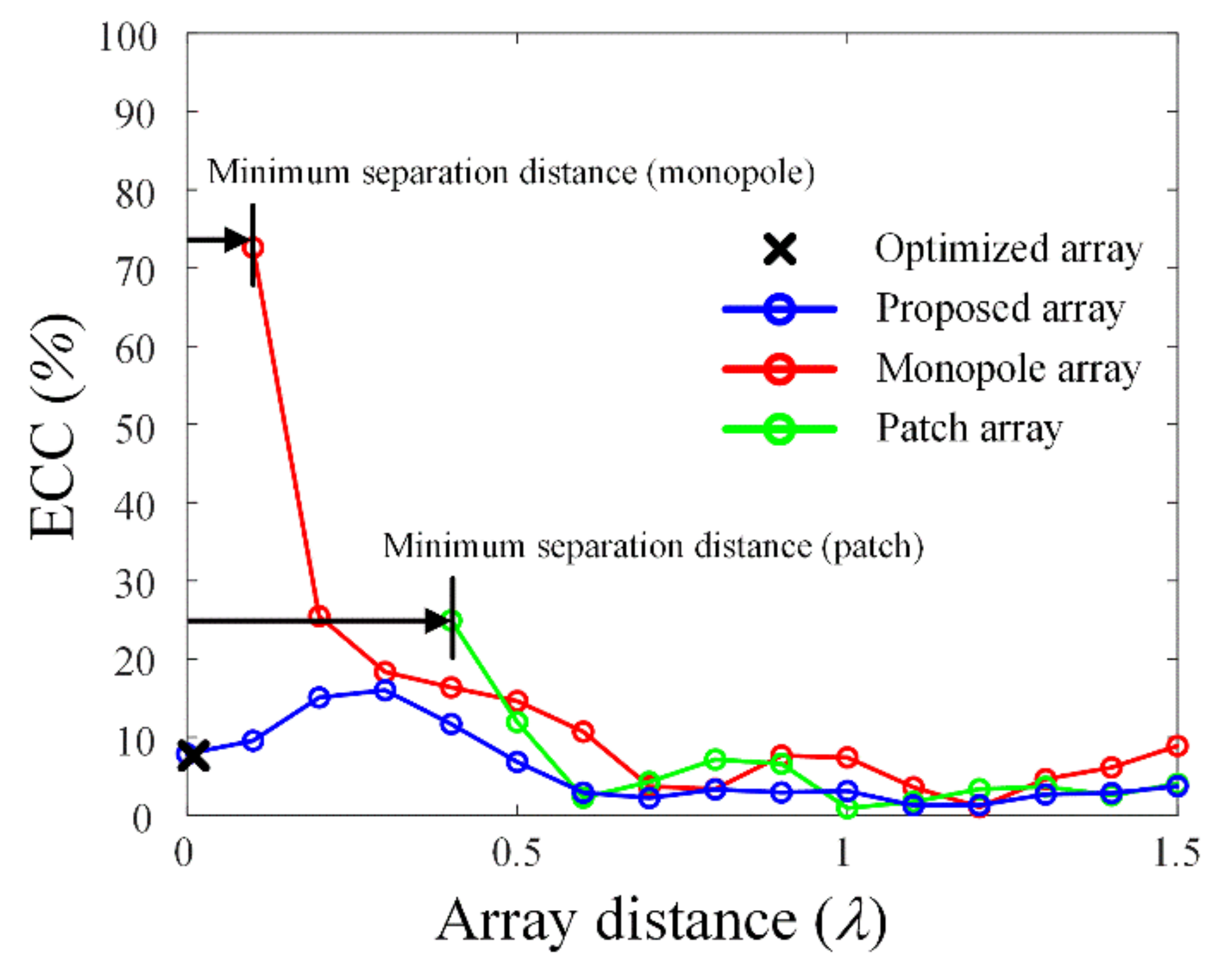
2. Proposed Array Antenna
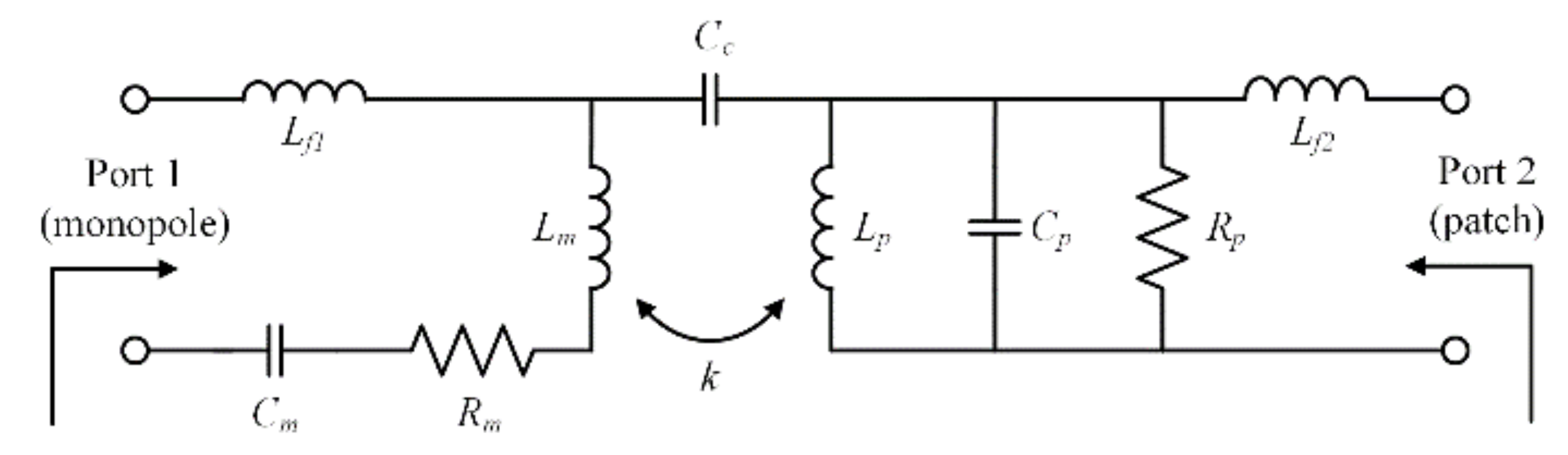
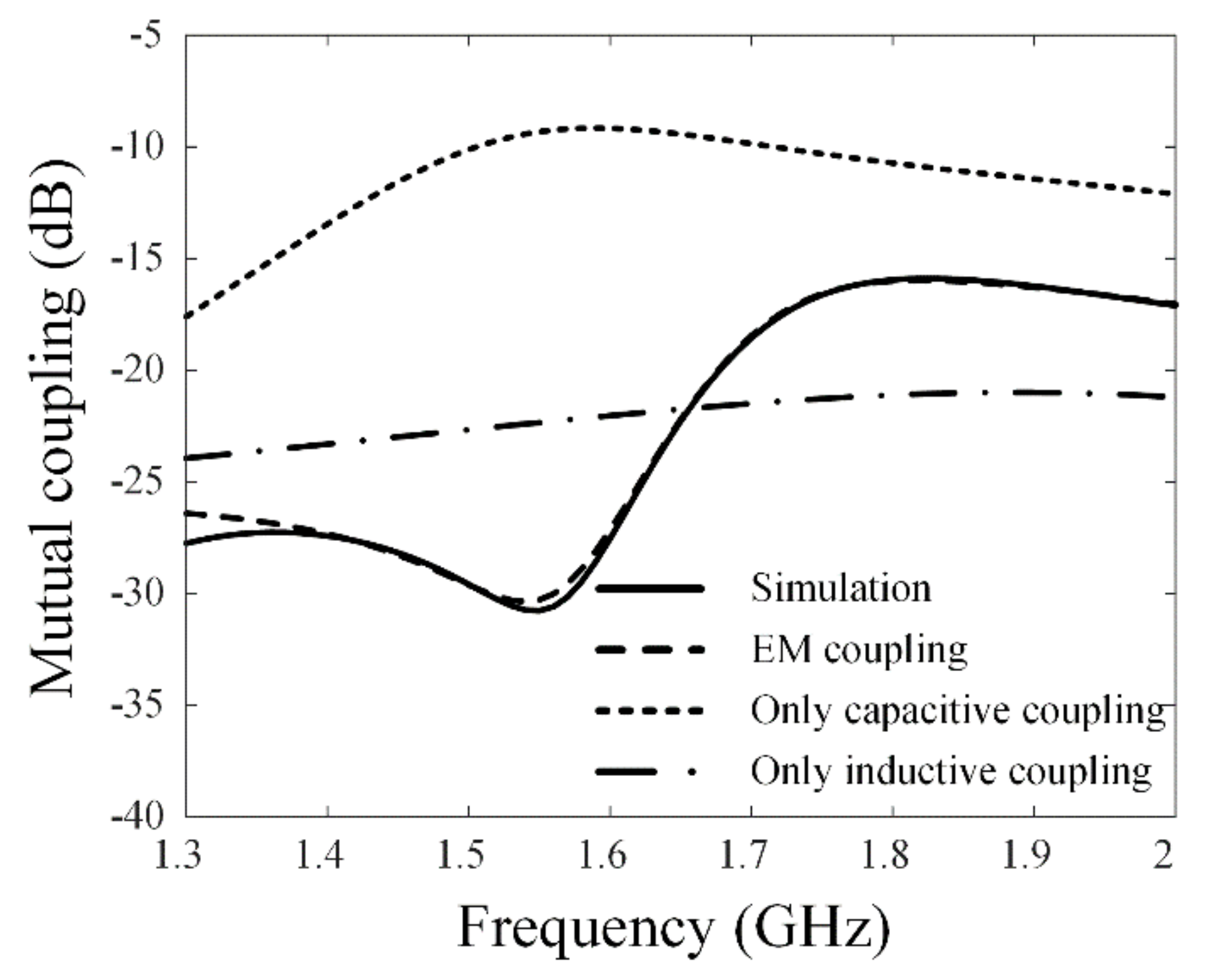
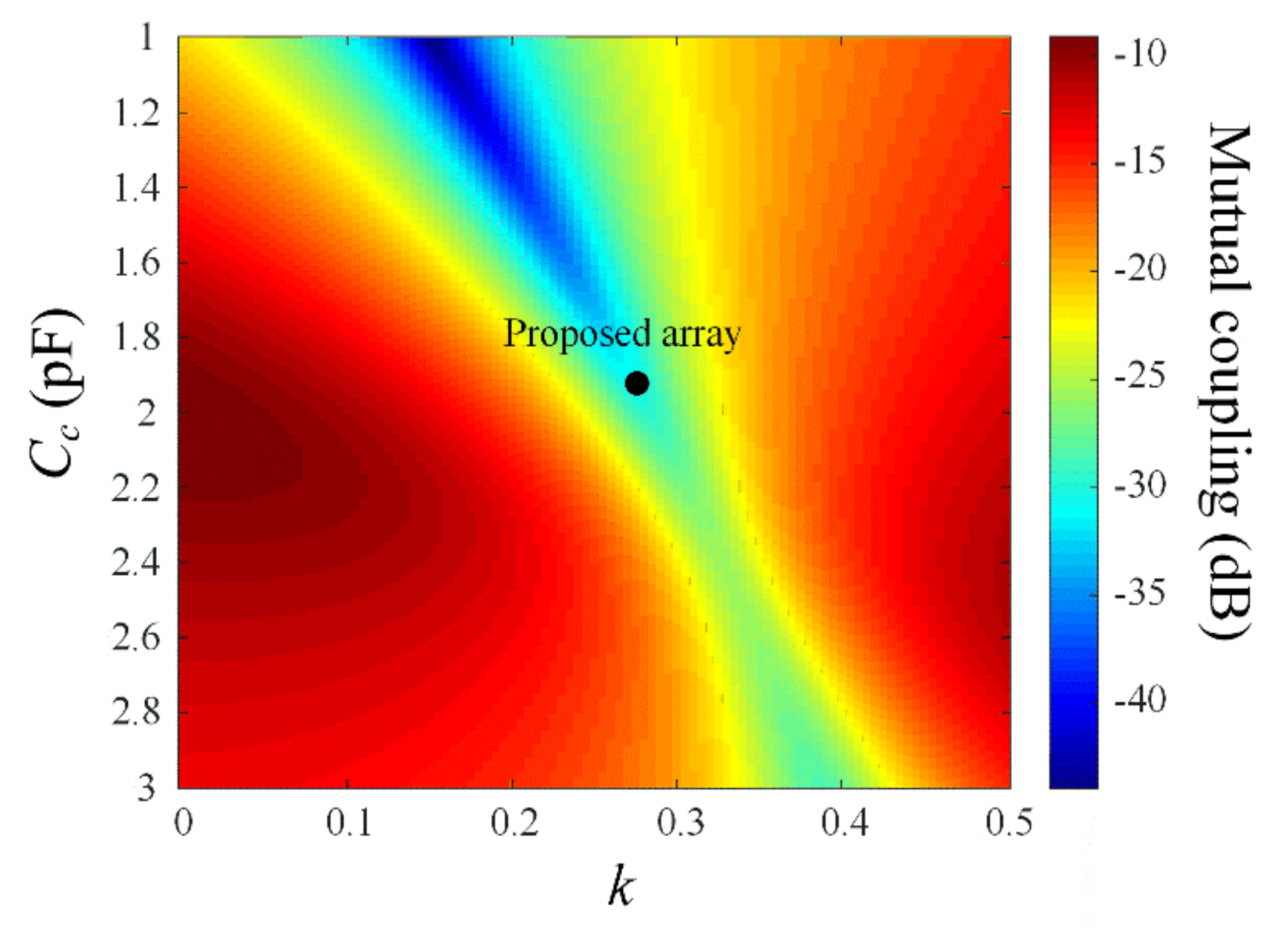
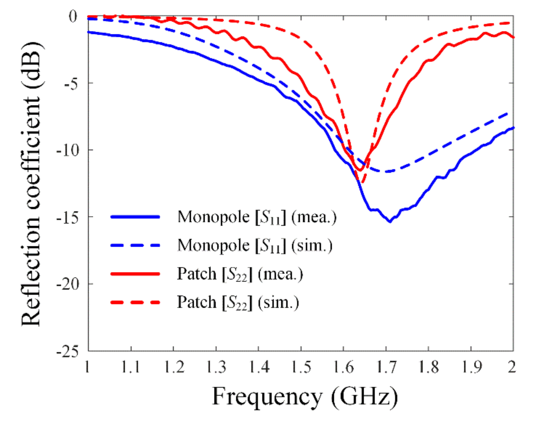
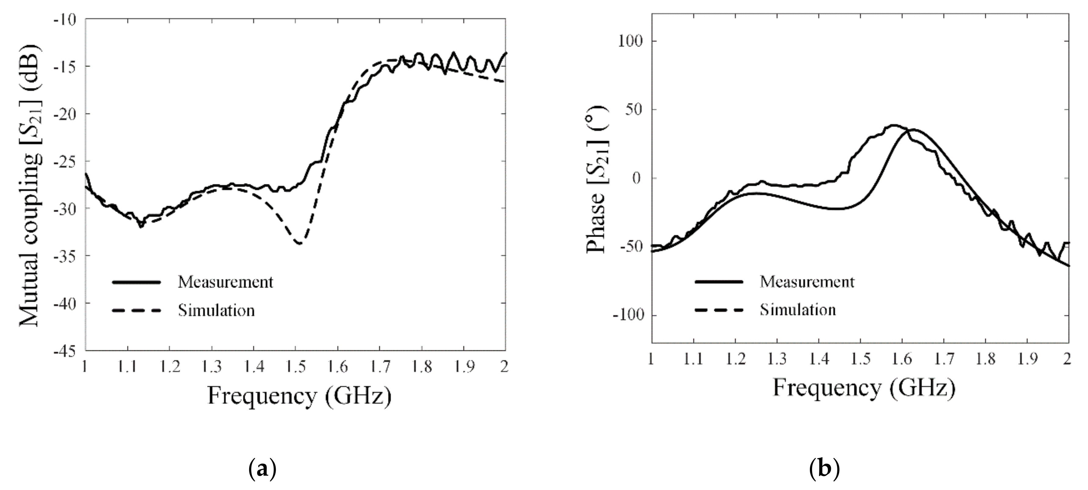
Figure 1 shows our design approach and geometry of the proposed array antenna with two radiators consisting of a patch and a monopole wire, where the two radiators share a common square ground plate with a width of lg. The first array element, the patch radiator, is designed to form a rectangular ring shape with inner and outer widths of w and l, which is printed on a thick FR-4 cuboid substrate (εr = 4.5, tanδ = 0.018) with a thickness of t. Another array element, the monopole wire antenna of a length of h, is located in the center of the ground plate, and the two ports of the array elements fed by SMA connectors have an extremely narrow distance d from each other. This proposed array geometry can control the mutual coupling between two elements by adjusting the antenna parameters t and w, while maintaining good matching characteristics for both elements. Notice that in terms of the antenna geometry, this proposed array is different from the previous research [32,33,34,35,36,37,38,39] due to its distinct feeding mechanism and radiating modes.
To observe the electromagnetic coupling between the two elements according to the tuning parameters of t and w, we design an equivalent circuit model using a two-port network for the proposed array, as illustrated in Figure 2. In this circuit model, two ports of 50-Ω impedance are connected directly to both elements, which are fed via pins represented by inductances of Lf1 and Lf2. For the elements, the monopole is expressed by a series circuit of Rm, Lm, and Cm, and the patch is composed of the parallel lumped elements of Rp, Lp, and Cp. The monopole and patch circuits are coupled through the series coupling capacitance Cc and the inductive coupling coefficient k. The mutual couplings of CC and k can be adjusted by the array geometry parameters of h and w. Detailed values of the lumped elements are Lf1 = 13.8 nH, Lf2 = 0.36 nH, Lm = 6.6 nH, Lp = 0.38 nH, Rm = 5.1 Ω, Rp = 11 Ω, Cm = 30.8 pF, Cp = 16.9 pF, Cc = 2.1 pF, and k = 0.28. Figure 3 presents a comparison of mutual coupling effects of the proposed arrays according to the electric and magnetic coupling strengths. The solid line indicates the simulation result of the mutual coupling for the proposed array, and the dashed line is calculated from the designed circuit model using both electric and magnetic couplings. The mutual couplings after removing either the inductive coupling coefficient k or the capacitive coupling Cc are specified by dotted and dash-dotted lines, respectively. For a more precise observation of the electromagnetic coupling effects, we calculate Equation (1) of the mutual couplings at the target frequency (1.6 GHz) in accordance with the variations of Cc and k from the circuit model, and the result is shown in Figure 4:
S 12 C c , k = 1.5 + j 3.8 10 11 C c + 1.2 j 2.4 k + C c k 2 2.0 j 3.9 10 11 3.7 + j 3.2 10 12 C c + 7.6 + j 4 10 11 C c k + 2.5 + j 5.9 10 12 C c k 2 + 0.1 j 4.4 k 2 + 8.6 j 4.2 .
In addition, we examine the relationships among the coupling elements and the antenna geometry. Figure 5a,b illustrate the coupling capacitance Cc and coefficient k, respectively, according to the adjustment of the width w for the inner patch and the thickness t for the thick substrate. These two parameters can easily control the coupling capacitance from 0.4 pF to 2 pF and the coupling coefficient from 0.35 to 0.85. Furthermore, to derive the experimental Formulas (2) and (3) of Cc and k, the resulting curves are fitted by the summation of the exponential and polynomial equations using the nonlinear least square solutions. The detailed coefficients of the fitted curves are a0 = 2.5, a1 = 0.05, a2 = 0.2, a3 = −0.02, b0 = 1.6, b1 = 0.01, b2 = 0.2, b3 = −0.002, b4 = 0.4, b5 = −0.05, and b6 = −0.02.
C c w , t = a 0 + a 1 exp a 2 w + a 3 w t ,
k w , t = b 0 + b 1 exp b 2 w + b 3 exp b 4 t + b 5 w + b 6 t .
The results demonstrate that such adjustments of the proposed antenna geometry enable simultaneous achievement of the low mutual coupling and good impedance matching. Besides, each element with perpendicular current directions can provide near orthogonal radiation patterns with a low pattern correlation due to the apparent modal difference between them. These low pattern correlations can also be maintained since the active element patterns for individual elements are similar to the single element patterns of the monopole and patch antennas. To further enhance the array performance, we optimize the detailed array antenna parameters using the full-wave electromagnetic (EM) simulation software of WIPL-D [42] at the target frequency of 1.6 GHz, where the optimized antenna can be applied to signal reception applications such as GPS, global navigation satellite system (GNSS), and satellite digital audio radio service (SDARS). The detailed optimized parameters are l = 41.2 mm, w = 14.2 mm, ls = 60 mm, t = 10.5 mm, lg = 200 mm, h = 43.7 mm, and d = 14.4 mm. Figure 6 shows the photographs of the fabricated array antenna.
To confirm the feasibility of the proposed structure, the antenna characteristics, such as the reflection coefficients, radiation patterns, and gains, are measured in a full anechoic chamber. Figure 7 represents the measured and simulated reflection coefficients, where the blue and red lines indicate the array elements of the monopole and patch, respectively. Both array elements show low reflection coefficients of −10 dB and −10.7 dB for the monopole and patch elements at 1.6 GHz, respectively, where the measured results are in good agreement with the simulations. Figure 8 provides magnitude and phase response of the mutual coupling between the two feeding ports as a function of frequency. At 1.6 GHz, the measured magnitude and phase of the mutual coupling are −20.7 dB and 37°, respectively, and those by simulation are −21.1 dB and 31.4°, which maintains low mutual coupling values even with an extremely close interport spacing. Figure 9 represents the maximum gains obtained in the upper hemisphere, and the measured peak gains of the monopole and patch elements are 3.8 dBi and 6.1 dBi. Figure 10a,d present measured and simulated 2D active element patterns of the monopole and patch elements. They illustrate co- and cross-polarization in zx- and zy-planes (H- and E-planes) at 1.6 GHz. Note that the shapes of the active element patterns are noticeably similar to the radiation patterns of the standalone monopole and patch antennas, even though the two antennas are very close to each other. The patch element shows half power beam widths of 76.1° and 85.2° in zx- and zy-planes, respectively. The maximum gain of the patch element is obtained by slightly steering toward θ = 5°, while the monopole element has the peak radiation gain at θ = −45°. The resulting antenna characteristics demonstrate that the proposed two-element array antenna can maintain independent radiation patterns with high isolation and low correlation between array elements, even with the narrow array spacing. Figure 11 illustrates the measured and simulated results of the array radiation patterns for the proposed array in zx- and zy-planes. The total radiation pattern is calculated by the summation of the monopole and patch element patterns having the same weights. From these results, the peak gains of the measurement and simulation in zx-plane are 4.6 dBi and 5.3 dBi, respectively, and those in zy-plane are 2.9 dBi and 2.7 dBi, respectively. Minimum measured cross-polarization levels of −31.62 dBi and −19.3 dBi in zx- and zy-planes are also observed. Though the total array radiation pattern of the proposed array is different from the conventional regular element array, the proposed array can provide sufficient nulling performances in a practical nulling application, which will be discussed in Section 3.2.

3. Analysis

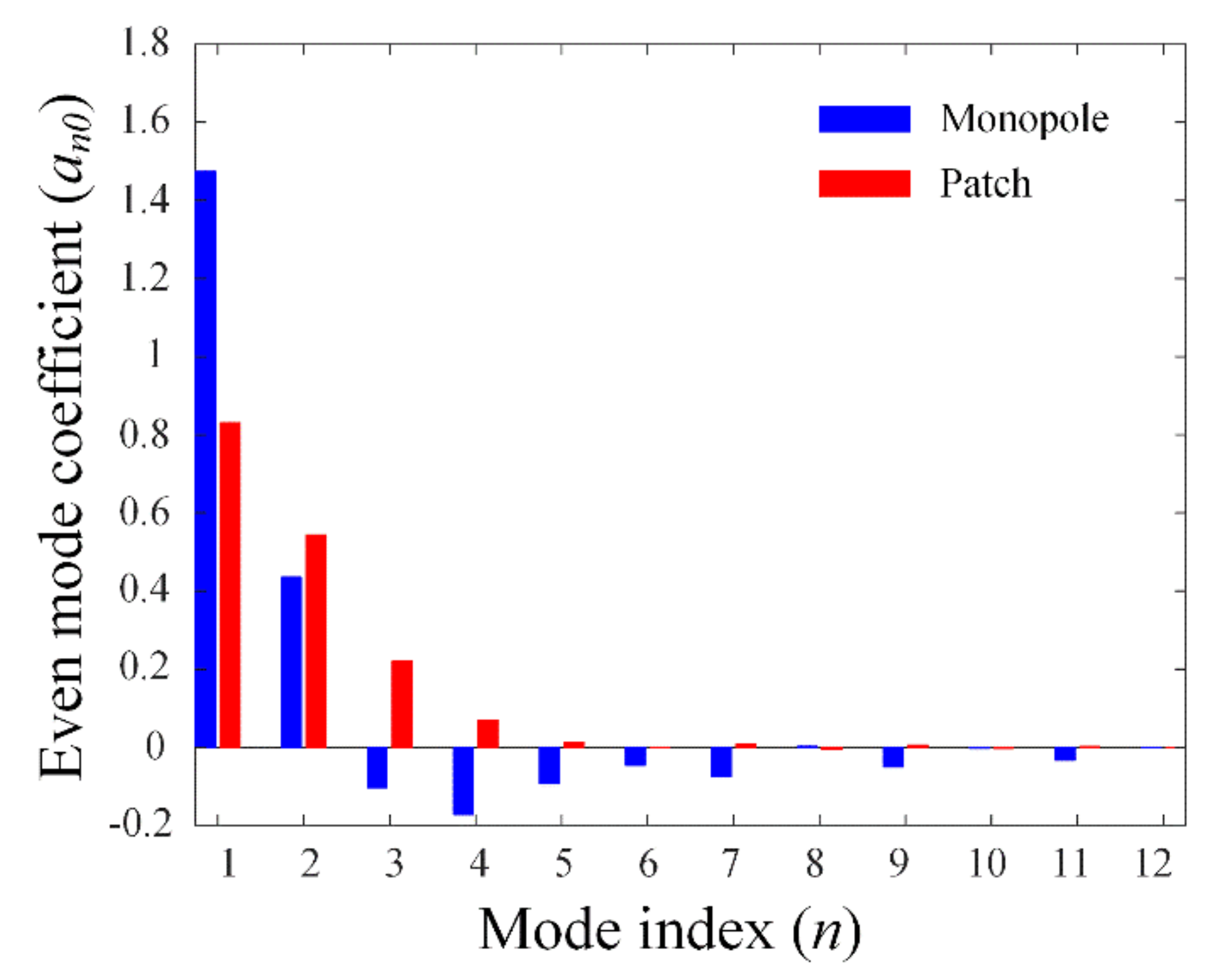
3.1. Spherical Mode Decomposition

To examine the radiating principle of the proposed array with low pattern correlation, we conduct spherical mode decomposition for the radiation patterns of the two antenna elements using a data-fitting method with the following steps. The first step obtains each active element pattern in the directions of θ and φ (361 × 30 points). Then, in the far-field region, each active pattern is expanded using the orthonormal spherical harmonics with even and odd modal coefficients [43].
Y n m e θ , ϕ = ε m 2 n + 1 2 π n m ! n + m ! 1 / 2 P n m cos θ cos m ϕ ,
Y n m o θ , ϕ = ε m 2 n + 1 2 π n m ! n + m ! 1 / 2 P n m cos θ sin m ϕ ,
E t o t = n = 0 N m = 0 n [ a n m Y n m e θ , ϕ + b n m Y n m o θ , ϕ ] .
The even and odd orthonormal harmonics of Y n m e and Y n m o contain the associated Legendre function according to the angles of θ and φ, where εm is Neumann’s number (1 for m = 0, and 2 for m > 0). The total electric field Etot is defined by the combinations of the even and odd coefficients of anm and bnm with the harmonics (n = 0, 1, 2 … N and m = 0, 1, 2 … n). The maximum mode number N is set to 12, and spherical mode decomposition for each active element pattern is conducted to obtain the unknown coefficients anm and bnm using the nonlinear least square method. In both element patterns of the proposed array, the coefficient anm is observed as much larger than bnm; therefore, the even mode coefficients should be examined more carefully to observe the modal characteristics of the active element patterns. In particular, among the resulting coefficients (anm) for both elements, the coefficients with an index of m = 0 predominantly determine the shape of the radiation patterns. Figure 12 shows the coefficient values of an0 versus the mode index n for the monopole and patch elements. The monopole element has a zero mode as the dominant mode, while a null pattern on the z-axis can be generated with negative coefficients in the second or higher modes. By contrast, most modal coefficients for the patch element are positive and significantly different from those of the monopole element. We propose the MDM to observe the modal difference between two antennas in a quantitative value. Herein, all mode coefficients of each antenna are normalized by the maximum coefficient value of the two antennas as written in Equation (7). Then, we calculate the MDM based on the average deviation of the normalized mode coefficients between the two antennas, as shown in Equation (8).
M n m 1 = a n m 1 max a n m 1 , a n m 2 , M n m 2 = a n m 2 max a n m 1 , a n m 2 ,
M D M = 2 N + 1 N + 2 n = 0 N m = 0 n M n m 1 M n m 2 ,
where the superscript 1 and 2 indicate the number of the antenna ports. The MDMs of 0.704, 0.307, and 0.219 are obtained for the proposed array, the patch array, and the monopole array, respectively. Note that, the high MDM means an obvious difference exists in the radiating pattern modes of the two antennas. Therefore, the results demonstrate that the low pattern correlation can be maintained for the proposed two-element array, even with an extremely narrow interelement spacing.
To confirm the pattern correlation between the two elements, we examine the ECCs of the proposed array compared to the conventional two-element patches and monopoles in terms of the interelement spacing. The interelement spacing of the proposed antenna is adjusted in the way of increasing the distance between two ports, as shown in Figure 13. Then, we calculate ECCs by S-parameters and radiation efficiencies applying Equation (9) introduced in [44] as follows:
ρ E C C = S 11 S 12 * + S 21 S 22 * 1 S 11 2 S 21 2 1 S 22 2 S 12 2 η 1 η 2 ,
where Sij (i = 1, 2 and j = 1, 2) is the complex S-parameter for each array port, and ηk (k = 1, 2) is the radiation efficiency of the observing antenna. Figure 14 illustrates the ECCs depending on the interelement spacing in wavelength for the three types of the two-element arrays. The blue, red, and green lines with circular markers designate the proposed, monopole, and patch arrays, respectively. We obtain the ECC values by simply increasing the interelement spacing of d between the two ports of the proposed array. In particular, when the distance becomes larger than half the size of the patch element, the two ports are separated by some distance and share a common ground. The proposed array can maintain the low ECC levels below 16% despite decreasing the port spacing between the elements. However, the patch and monopole array antennas require minimum separation distances due to the physical antenna size, and the ECC levels increase drastically as the distance between the array antennas narrows.

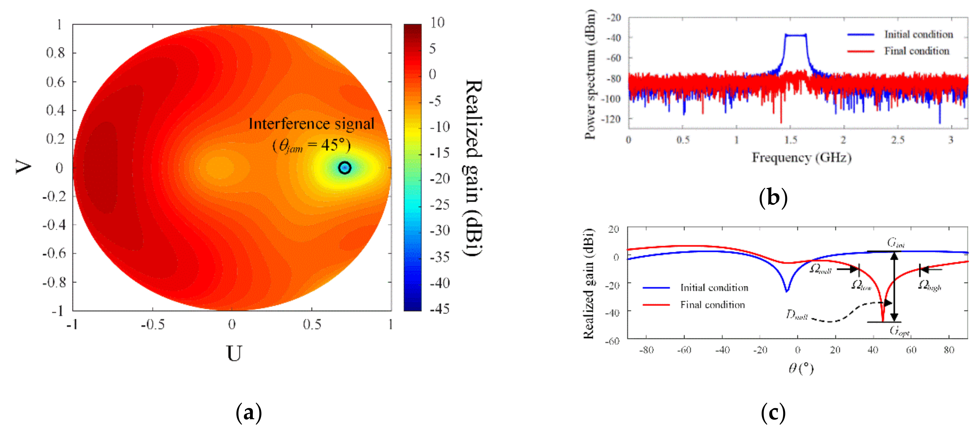
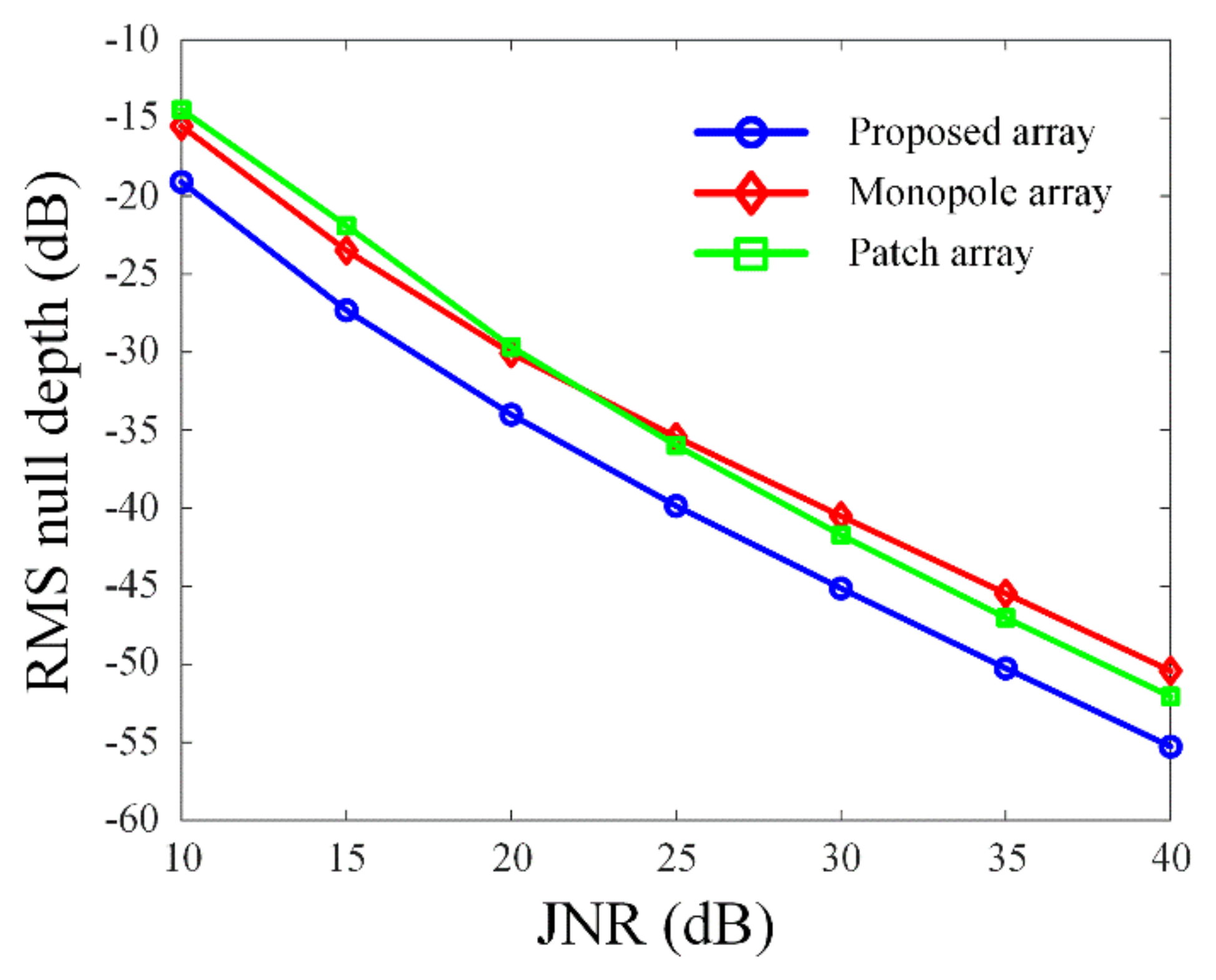
3.2. Adaptive Null Steering Performance

In general, the radiation patterns of the array antenna elements are constructively and destructively added with adequate weights to construct a beam-forming pattern at the wanted signal direction and a beam-nulling pattern at the interference signal direction. From this common principle of a null pattern formation, we build a simulation model for an antijamming system using a conventional PI algorithm in order to estimate a practical pattern nulling performance. In the algorithm, the signal received by the proposed two-element array can modeled as
X ¯ = A ¯ S S ¯ + A ¯ J J ¯ + N ¯ ,
where X ¯ is a column vector of the received signal, while S ¯ and J ¯ are column vectors of the wanted and jamming signals. A s ¯ and A J ¯ are the steering vector matrices of the wanted and jamming signals. N ¯ is the vector of the additive white Gaussian noise to model a typical communication environment. We then apply the conventional nulling technique of the PI algorithm to adjust the weight vector W ¯ with the received signals in order to suppress the interference. The output signal is y = W ¯ H X ¯ , which is weighted and summed of all the received signals, and we use the linearly constrained minimum variance (LCMV) method as a regular criterion to obtain the optimum weight vector of W ¯ o p t as follows [45,46]:
W ¯ o p t = R ¯ 1 h ¯ h ¯ T R ¯ 1 h ¯ ,
where R ¯ = E{ X ¯ X H } is the covariance matrix of the received signal, and h ¯ = [1, 0, …, 0]T is the common constraint matrix. For the interference mitigation scenario, we first suppose a scenario that the average powers of the wanted, interference, and noise signals are set to −83 dBm, −3 dBm, and −43 dBm, respectively. It is also assumed that the interference of the chirp signal arrives at an elevation angle θjam = 45° at the frequencies ranging from 1.45 GHz to 1.65 GHz. This interference signal is then mitigated by the nulling process using the optimum weight W ¯ o p t to examine the null depth, width, and DOA error.
D n u l l = G o p t G i n i ,
Ω n u l l = Ω h i g h Ω l o w g a i n = 10   dBi ,
Δ θ n u l l = θ o p t θ j a m .
The null depth Dnull is obtained by the difference between the initial array gain Gini before the nulling process and the final array gain Gopt after the PI algorithm when the system is exposed to the same chirp interference signals. The null width Ωnull is achieved by the angular difference between two points (Ωhigh, Ωlow) in the optimized nulling pattern where the gain is −10 dBi. We calculate the null DOA error Δθnull from the difference between the optimal null angle θopt and the actual jamming angle θjam. Figure 15a shows the optimized null pattern of the proposed array in the UV domain when the interference signal is at 45°. Figure 15b illustrates the initial and final power spectrums, confirming that the chirp interference signal can be suppressed significantly by applying the optimum null weights for the proposed antenna. The optimum null pattern of the proposed array has the Dnull of −47.7 dB with a null width Ωnull of 33.2°, as presented in Figure 15c. We also obtain the simulated cross-polarization levels of the proposed antenna in zx- and zy-planes compared to those of the conventional two-element patch array antenna. The average cross-polarization levels over all elevation angles of both array antennas were less than −108 dBi, and the cross-polarization level of the proposed array is maximally 14.7 dB higher than that of the conventional patch array. From these results, although the proposed array shows higher cross-polarization levels and slightly lower array gains than the conventional patch array, the interelement spacing of the proposed array can be miniaturized to 0.08λ.
Such nulling performances of the proposed array are observed in comparisons with the conventional monopole and patch arrays. The interelement spacing for the monopole array is set to 0.1λ, and for the patch array is 0.4λ. They are the narrowest possible interelement spacings for the two array elements. For the simulations, the direction of the interference angle is varied from −60° to 60° with an interval of 1°, and the jammer power to noise power ratio (JNR) is changed from 10 dB to 40 dB with the independent gaussian random noise created by 50 iterations. Figure 16 represents the comparisons of the root-mean-square (RMS) null depths in terms of JNR for the proposed, conventional monopole, and patch arrays. The proposed array with the very close interport spacing of 0.08λ can maintain the deepest null depth compared to those of the conventional monopole and patch arrays, and the null depth of −54.3 dB is observed at a JNR of 40 dB. Note that, in this interference mitigation, it is essential to not only have a deep null depth but also to consider other important factors such as low blind region for receiving wanted signals [47] and fast iteration time to form a null pattern [11,47]. Figure 17 shows the RMS null widths versus JNR; the narrowest null width of 27.6° is obtained when the JNR increases above 15 dB. Figure 18 presents the RMSE comparisons of the null DOA. Although the proposed array has the higher RMSE under a JNR of 20 dB, the RMSE of less than 0.8° can be sustained above a JNR of 20 dB. To observe the null steering capability in a wide scan angle, the simulations of the null depths in accordance with θjam varied from 0° to 90° at a JNR of 15 dB are also conducted, and the results of the proposed array are compared to the conventional patch arrays. The average null depth of the proposed array is 3.1 dB higher than that of the patch array in high elevation angle (0° ≤ θjam ≤ 12°). On the other hand, in the low elevation angle (13° ≤ θjam ≤ 90°), the proposed antenna has an 8.7 dB deeper average null depth than that of the patch array. The results demonstrate that the proposed two-element array is suitable for achieving the required null pattern characteristics with an extremely narrow array distance due to the modal difference, the low pattern correlation, and the high isolation between the array elements.

4. Conclusions

We proposed a novel design of a two-element array antenna on an electrical thick substrate with an extremely narrow array distance, where the patch and monopole radiators had a modal difference in the radiation pattern, causing high isolation and a low correlation between the array elements. The proposed array was fabricated to measure the characteristics of each element. Both array elements provided low reflection coefficients of −10 dB and −10.7 dB for the monopole and patch elements, respectively, at 1.6 GHz; the measured mutual coupling between the two feeding ports was −20.7 dB, and that of the simulation was −21.1 dB. The measured maximum gains obtained in the upper hemisphere were 3.8 dBi and 6.1 dBi for the monopole and patch elements, respectively. The array radiation pattern was calculated by superposing the monopole and patch element patterns with the same weight. By measurement, the peak gains in zx- and zy- planes were 4.6 dBi and 2.9 dBi, respectively, while minimum cross-polarization levels of −31.62 dBi and −19.3 dBi in zx- and zy-planes were observed. In the spherical mode decomposition of the antenna pattern, the monopole element had the zero mode as the dominant mode, with the negative coefficient values after the second or higher order modes compared to the patch element mostly having the positive coefficients of the spherical harmonic modes. We also proposed the MDM to observe the modal difference between two antennas. MDMs of 0.704, 0.307, and 0.219 were obtained for the proposed array, the patch array, and the monopole array, respectively. In addition, the proposed array could maintain the low ECC levels under 16% despite decreasing the port spacing between the elements. To verify the proposed array in a practical pattern nulling application, we investigated the antijamming performance using a PI algorithm, and the null depth of −47.7 dB with the null width of 33.2° was obtained when the interference signal arrived at the elevation angle of 45°. In comparison with the conventional monopole and patch arrays, the proposed array also obtained the RMS null depth of −54.3 dB, the RMS null width of 27.6°, and the RMSE of 0.8°. The results demonstrate that the proposed array antenna provided high nulling performances and maintained an extremely narrow array distance.

Author Contributions

Conceptualization, T.H.L., B.-J.J. and H.C.; methodology, T.H.L. and H.C.; software, T.H.L.; validation, T.H.L., B.-J.J. and H.C.; formal analysis, T.H.L. and H.C.; investigation, T.H.L. and B.-J.J.; resources, T.H.L.; data curation, T.H.L.; writing—original draft preparation, T.H.L. and H.C.; writing—review and editing, T.H.L., B.-J.J., and H.C.; visualization, T.H.L.; supervision, H.C.; project administration, B.-J.J.; funding acquisition, B.-J.J. and H.C. All authors have read and agreed to the published version of the manuscript.

Funding

This work was supported by the Samsung Research Funding Center of Samsung Electronics under project number SRFC-IT1801-06.

Conflicts of Interest

The authors declare no conflict of interest.

References

  1. Ban, Y.-L.; Li, C.; Sim, C.-Y.-D.; Wu, G.; Wong, K.-L. 4G/5G multiple antennas for future multi-mode smartphone applications. IEEE Access 2016, 4, 2981–2988. [Google Scholar] [CrossRef]
  2. Hussain, R.; Alreshaid, A.T.; Podilchak, S.K.; Sharawi, M.S. Compact 4G MIMO antenna integrated with a 5G array for current and future mobile handsets. IET Microw. Antennas Propag. 2017, 11, 271–279. [Google Scholar] [CrossRef] [Green Version]
  3. Lim, C.-H.; Wan, Y.; Ng, B.-P.; See, C.-M. A Real-time indoor wifi localization system utilizing smart antennas. IEEE Trans. Consum. Electron. 2007, 53, 618–622. [Google Scholar] [CrossRef]
  4. Lee, H.; Yoon, M.; Nam, S. Cylindrical tightly coupled dipole array antenna. J. Electromagn. Eng. Sci. 2019, 19, 122–129. [Google Scholar] [CrossRef]
  5. Kwon, T.-S.; Lee, J.-G.; Lee, J.-H. Null steering of circular array using array factor for GPS anti-jam. J. Electromagn. Eng. Sci. 2018, 18, 267–269. [Google Scholar] [CrossRef] [Green Version]
  6. Yoon, J.H.; Yoon, Y.J. Bandwidth enhancement of single-layer microstrip reflectarrays with multi-dipole elements. J. Electromagn. Eng. Sci. 2019, 19, 130–139. [Google Scholar] [CrossRef]
  7. Kim, J.; Song, S.C.; Shin, H.; Park, Y.B. Radiation from a millimeter-wave rectangular waveguide slot array antenna enclosed by a Von Karman radome. J. Electromagn. Eng. Sci. 2018, 18, 154–159. [Google Scholar] [CrossRef] [Green Version]
  8. Morton, Y.T.; Miller, M.; Tsui, J.; Lin, D.; Zhou, Q. GPS civil signal self-interference mitigation during weak signal acquisition. IEEE Trans. Signal Process. 2007, 55, 5859–5863. [Google Scholar] [CrossRef] [Green Version]
  9. Tao, M.; Zhou, F.; Zhang, Z. Wideband interference mitigation in high-resolution airborne synthetic aperture radar data. IEEE Trans. Geosci. Remote. Sens. 2016, 54, 74–87. [Google Scholar] [CrossRef]
  10. Lambert, J.R.; Balanis, C.A.; DeCarlo, D. Spherical cap adaptive antennas for GPS. IEEE Trans. Antennas Propag. 2009, 57, 406–413. [Google Scholar] [CrossRef]
  11. Byun, G.; Choo, H.; Kim, S. Improvement of pattern null depth and width using a curved array with two subarrays for CRPA systems. IEEE Trans. Antennas Propag. 2015, 63, 2824–2827. [Google Scholar] [CrossRef]
  12. Byun, G.; Choo, H.; Kim, S. Design of a small arc-shaped antenna array with high isolation for applications of controlled reception pattern antennas. IEEE Trans. Antennas Propag. 2016, 64, 1542–1546. [Google Scholar] [CrossRef]
  13. Lee, T.; Lee, D.-H.; Choo, H.; Byun, G. A method of substrate shaping to improve gain of active-element pattern for small arrays. Antennas Wirel. Propag. Lett. 2017, 16, 1601–1604. [Google Scholar] [CrossRef]
  14. Maloney, J.A.; Kwon, D.-H.; Keller, S.D.; Janaswamy, R. Realistic GPS coverage prediction for dual-polarized controlled reception pattern antennas. Antennas Wirel. Propag. Lett. 2017, 16, 1907–1910. [Google Scholar] [CrossRef]
  15. Rezazadeh, N.; Shafai, L. A controlled reception pattern antenna array with dual-mode circular microstrip antenna elements for increased angular availability. IEEE Trans. Antennas Propag. 2018, 66, 2594–2598. [Google Scholar] [CrossRef]
  16. Li, Q.; Wang, W.; Xu, D.; Wang, X. A robust anti-jamming navigation receiver with antenna array and GPS/SINS. IEEE Commun. Lett. 2014, 18, 467–470. [Google Scholar] [CrossRef]
  17. Lau, B.K.; Andersen, J.B. Simple and efficient decoupling of compact arrays with parasitic scatterers. IEEE Trans. Antennas Propag. 2012, 60, 464–472. [Google Scholar] [CrossRef] [Green Version]
  18. Mak, A.C.K.; Rowell, C.R.; Murch, R.D. Isolation enhancement between two closely packed antennas. IEEE Trans. Antennas Propag. 2008, 56, 3411–3419. [Google Scholar] [CrossRef]
  19. Li, Z.; Du, Z.; Takahashi, M.; Saito, K.; Ito, K. Reducing mutual coupling of MIMO antennas with parasitic elements for mobile terminals. IEEE Trans. Antennas Propag. 2012, 60, 473–481. [Google Scholar] [CrossRef]
  20. Ahn, D.; Park, J.-S.; Kim, C.-S.; Kim, J.; Qian, Y.; Itoh, T. A design of the low-pass filter using the novel microstrip defected ground structure. IEEE Trans. Microw. Theory Tech. 2001, 49, 86–93. [Google Scholar] [CrossRef]
  21. Hur, J.; Choo, H.; Byun, G. Design of a small controlled reception pattern antenna array with a single-layer coupled feed structure for enhanced bore-sight gain and a matching bandwidth. Electromagnetics 2017, 37, 297–309. [Google Scholar] [CrossRef]
  22. Wang, K.; Mauermayer, R.A.M.; Eibert, T.F. Compact two-element printed monopole array with partially extended ground plane. Antennas Wirel. Propag. Lett. 2014, 13, 138–140. [Google Scholar] [CrossRef]
  23. Lee, J.-Y.; Kim, S.-H.; Jang, J.-H. Reduction of mutual coupling in planar multiple antenna by using 1-D EBG and SRR structures. IEEE Trans. Antennas Propag. 2015, 63, 4194–4198. [Google Scholar] [CrossRef]
  24. Sievenpiper, D.; Zhang, L.; Broas, R.F.; Alexopolous, N.G.; Yablonovitch, E. High-impedance electromagnetic surfaces with a forbidden frequency band. IEEE Trans. Microw. Theory Tech. 1999, 47, 2059–2074. [Google Scholar] [CrossRef] [Green Version]
  25. Yang, F.; Rahmat-Samii, Y. Microstrip antennas integrated with electromagnetic band-gap (EBG) structures: A low mutual coupling design for array applications. IEEE Trans. Antennas Propag. 2003, 51, 2936–2946. [Google Scholar] [CrossRef] [Green Version]
  26. Yang, S.; Gosling, I.G.; Tan, S.H.; Sorwar, M.G. TLM analysis of the mutual coupling of microstrip patch antenna arrays. IEE Proc. Microw. Antennas Propag. 2000, 147, 207–210. [Google Scholar] [CrossRef]
  27. Hur, J.; Byun, G.; Choo, H. Design of a planar periodic lossy magnetic surface to improve active array patterns with enhanced isolation. IET Microw. Antennas Propag. 2018, 12, 2383–2389. [Google Scholar] [CrossRef]
  28. Bell, J.M.; Iskander, M.F.; Lee, J.J. Ultrawideband hybrid EBG/ferrite ground plane for low-profile array antennas. IEEE Trans. Antennas Propag. 2007, 55, 4–12. [Google Scholar] [CrossRef]
  29. Labadie, N.R.; Sharma, S.K.; Rebeiz, G.M. A novel approach to beam steering using arrays composed of multiple unique radiating modes. IEEE Trans. Antennas Propag. 2015, 63, 2932–2945. [Google Scholar] [CrossRef] [Green Version]
  30. Narbudowicz, A.; Ammann, M.J. Low-cost multimode patch antenna for dual MIMO and enhanced localization use. IEEE Trans. Antennas Propag. 2018, 66, 405–408. [Google Scholar] [CrossRef] [Green Version]
  31. Herscovici, N.; Christodoulou, C.; Rajo-Iglesias, E.; Quevedo-Teruel, O.; Sanchez-Fernandez, M. Compact multimode patch antennas for mimo applications [Wireless Corner]. IEEE Antennas Propag. Mag. 2008, 50, 197–205. [Google Scholar] [CrossRef]
  32. Narbudowicz, A.; Ammann, M.J.; Plotka, M.; Kulas, L.; Nyka, K.; Rzymowski, M. Compact antenna for digital beamforming with software defined radios. In Proceedings of the 2017 International Symposium on Antennas and Propagation (ISAP), Phuket, Thailand, 30 October–2 November 2017; pp. 1–2. [Google Scholar]
  33. Labadie, N.R.; Sharma, S.K.; Rebeiz, G.M. A circularly polarized multiple radiating mode microstrip antenna for satellite receive applications. IEEE Trans. Antennas Propag. 2014, 62, 3490–3500. [Google Scholar] [CrossRef]
  34. Labadie, N.R.; Sharma, S.K.; Rebeiz, G.M. Investigations on the use of multiple unique radiating modes for 2-D beam steering. IEEE Trans. Antennas Propag. 2016, 64, 4659–4670. [Google Scholar] [CrossRef]
  35. Han, T.-Y.; Huang, C.-T. Reconfigurable monopolar patch antenna. Electron. Lett. 2010, 46, 199–200. [Google Scholar] [CrossRef]
  36. Labadie, N.R.; Sharma, S.K.; Rebeiz, G. Multimode antenna element with hemispherical beam peak and null steering. In Proceedings of the 2012 IEEE International Symposium on Antennas and Propagation (APSURSI), Chicago, IL, USA, 8–14 July 2012; pp. 1–2. [Google Scholar]
  37. Narbudowicz, A.; Ammann, M.J.; Heberling, D. Electrically small antenna with switchless pattern reconfiguration. In Proceedings of the 2017 IEEE International Symposium on Antennas and Propagation USNC/URSI National Radio Science Meeting, San Diego, CA, USA, 9–14 July 2017; pp. 1201–1202. [Google Scholar]
  38. Niroo-Jazi, M.; Denidni, T.A. A new triple-band circular ring patch antenna with monopole-like radiation pattern using a hybrid technique. IEEE Trans. Antennas Propag. 2011, 59, 3512–3517. [Google Scholar] [CrossRef]
  39. Narbudowicz, A.; Ammann, M.J.; Heberling, D. Switchless reconfigurable antenna with 360° steering. Antennas Wirel. Propag. Lett. 2016, 15, 1689–1692. [Google Scholar] [CrossRef]
  40. Chiu, C.-Y.; Cheng, C.-H.; Murch, R.D.; Rowell, C.R. Reduction of mutual coupling between closely-packed antenna elements. IEEE Trans. Antennas Propag. 2007, 55, 1732–1738. [Google Scholar] [CrossRef]
  41. Chattha, H.T. 4-port 2-element MIMO antenna for 5G portable applications. IEEE Access 2019, 7, 96516–96520. [Google Scholar] [CrossRef]
  42. WIPL-D Pro CAD 2019. Available online: http://www.wipl-d.com (accessed on 3 March 2020).
  43. Chen, Y.; Simpson, T. Radiation pattern analysis of arbitrary wire antennas using spherical mode expansions with vector coefficients. IEEE Trans. Antennas Propag. 1991, 39, 1716–1721. [Google Scholar] [CrossRef]
  44. Hallbjorner, P. The significance of radiation efficiencies when using S-parameters to calculate the received signal correlation from two antennas. Antennas Wirel. Propag. Lett. 2005, 4, 97–99. [Google Scholar] [CrossRef]
  45. Compton, R.T. The power-inversion adaptive array: Concept and performance. IEEE Trans. Aerosp. Electron. Syst. 1979, AES-15, 803–814. [Google Scholar] [CrossRef]
  46. Lang, R.; Xiao, H.; Li, Z.; Yu, L. A anti-jamming method for satellite navigation system based on multi-objective optimization technique. PLoS ONE 2017, 12, e0180893. [Google Scholar] [CrossRef] [PubMed] [Green Version]
  47. Byun, G.; Hyun, J.-C.; Seo, S.M.; Choo, H. Optimum Array Configuration to Improve Null Steering Time for Mobile CRPA Systems. J. Electromagn. Eng. Sci. 2016, 16, 74–79. [Google Scholar] [CrossRef] [Green Version]
Figure 1. Design approach and geometry of the proposed array antenna: (a) design approach of the proposed array antenna; (b) side view of the proposed array antenna.
Applsci 10 03916 g001
Figure 2. An equivalent circuit model with a two-port network for the proposed array.
Applsci 10 03916 g002
Figure 3. Comparison of mutual coupling performance effects of the proposed arrays according to the electric and magnetic coupling strengths.
Applsci 10 03916 g003
Figure 4. Mutual couplings in accordance with the variations of Cc and k.
Applsci 10 03916 g004
Figure 5. Coupling capacitance Cc and coefficient k according to the adjustment of w and t: (a) coupling capacitance Cc; (b) coupling coefficient k.
Applsci 10 03916 g005
Figure 6. Photographs of the fabricated array antenna: (a) isometric view; (b) bottom view.
Applsci 10 03916 g006
Figure 7. Simulated and measured reflection coefficients of the proposed array.
Applsci 10 03916 g007
Figure 8. Simulated and measured mutual coupling (S21) of the proposed array: (a) magnitude of mutual coupling; (b) phase of mutual coupling.
Applsci 10 03916 g008
Figure 9. Simulated and measured maximum gains in the upper hemisphere of the proposed array.
Applsci 10 03916 g009
Figure 10. Measured and simulated 2D co- and cross-polarization radiation patterns of the proposed array in the zy- and zx-planes at 1.6 GHz: (a) monopole element in the zy-plane (E-plane); (b) monopole element in the zx-plane (H-plane); (c) patch element in the zy-plane (E-plane); (d) patch element in the zx-plane (H-plane).
Applsci 10 03916 g010
Figure 11. Array radiation patterns of the proposed array antenna: (a) zx-plane (H-plane); (b) zy-plane (E-plane).
Applsci 10 03916 g011
Figure 12. The even mode coefficient an0 according to the mode n for monopole and patch element radiation patterns.
Applsci 10 03916 g012
Figure 13. Conceptual figures for the interelement spacing d: (a) d = 0.08λ; (b) d = 0.25λ; (c) d = 0.5λ.
Applsci 10 03916 g013
Figure 14. Comparisons of the ECCs for three types of array antennas.
Applsci 10 03916 g014
Figure 15. 3D and 2D null steering patterns of the proposed array with the power spectrum: (a) 3D radiation pattern in UV domain; (b) power spectrum with initial and final weights; (c) null performance parameters.
Applsci 10 03916 g015
Figure 16. Root-mean-square (RM) S null depth in terms of jammer power to noise power ratio (JNR) of the proposed array compared to the conventional patch and monopole arrays.
Applsci 10 03916 g016
Figure 17. RMS null width in terms of JNR of the proposed array compared to the conventional patch and monopole arrays.
Applsci 10 03916 g017
Figure 18. RMSE in terms of the JNR of the proposed array compared to the conventional patch and monopole arrays.
Applsci 10 03916 g018

