Abstract
Macro Fiber Composites (MFCs) exhibit significant potential in active control applications. These include vibration control for unmanned aerial vehicle wings and helicopter rotors. However, the high-voltage drive requirements of MFCs present challenges. The miniaturization of the controller is a mandatory condition in order not to affect the overall space utilization. Thus, this paper presents a specialized miniaturized high-voltage control system designed specifically for MFC actuators. The proposed system employs a mixed analog-digital modulation method (ADM). This method precisely regulates a discontinuous conduction mode flyback switch-mode power supply operating in current mode. The system achieves an adjustable high-voltage output range of -500 V to 1500 V. The mixed control system consists of several components. These include a switching power supply, a voltage divider circuit, a bleeder circuit, and a digital controller. Additionally, this high-voltage control system integrates with a Simulink software environment. The system is compact and lightweight. It also features high load capacity, high power, and excellent dynamic response. Moreover, it offers real-time control capabilities. Experimental validation on a high-aspect-ratio wing demonstrates that this control system achieves a vibration reduction effect of 65%. The miniaturized control system provides a valuable research base for vibration control studies.
1. Introduction
With the widespread use of large flexible structures in aerospace vehicles, prolonged vibrations can lead to fatigue failure, significantly reducing the lifespan of aerospace systems. To ensure stable long-term operation, it is essential to suppress the vibrations of these large flexible structures. Recently, vibration suppression has garnered increasing attention and research interest [1]. Smart structures are systems equipped with sensing, actuation, and control capabilities, offering innovative solutions for addressing the vibration issues of large flexible structures. Piezoelectric materials are an important part of intelligent structures. Among these materials, Macro Fiber Composites (MFC), invented by NASA’s Langley Research Center in 1996, consist primarily of piezoelectric ceramic fiber layers, interdigitated electrodes, and a polymer matrix. Compared to unidirectional piezoelectric ceramics, MFCs boast advantages such as strong actuation performance, light weight, and high flexibility. They can be easily adhered to various surfaces, including curved ones. Due to these exceptional properties, MFC actuators have attracted significant attention from researchers and are widely used in structural vibration control [2]. The MFC is used as an actuator to take advantage of its inverse piezoelectric effect. They operate within an asymmetric high-voltage range of −500 V to 1500 V. Designing a high-voltage drive circuit to meet this requirement is of great significance. Additionally, the need for miniaturization in development is another important factor to consider.
In the field of vibration control using MFC actuators, Guo et al. developed a laminated plate model that considers the anisotropic properties of MFC. They applied this model to control the vibrations of rotating plates, conducting static, dynamic, and modal analyses to study the effects of various parameters. Their simulation results demonstrated the capability of MFC actuators for vibration control [3]. Li et al. conducted active vibration control experiments on piezoelectric flexible beams under instantaneous and continuous disturbance conditions. Their results indicate that the vibrations of the flexible beams were effectively suppressed under various disturbances [4]. Zhou et al. proposed a self-feedback system based on MFC. At a resonant frequency of 67 Hz, the vibration suppression rate reached 82.09%. Their design is suitable for various thin-walled materials, such as carbon fiber plates, epoxy boards, and steel plates [5]. Luo et al. applied MFC to control bending and twisting vibrations in large, flexible, lightweight wing structures. Through ANSYS simulation analysis, they demonstrated the effectiveness of a current control system on the low-frequency modal responses of the wing structure [6]. Gao et al. employed MFC for the end vibration control of a flexible robotic arm. They introduced a novel multi-model switching adaptive control algorithm, using a cantilever beam with variable end mass as the flexible arm model. Both simulation and experimental results showed that their FXLMS-based multi-model adaptive control method demonstrated optimal vibration suppression capabilities [7]. The MFC actuators have made good progress in the field of structural vibration control. However, most of the control systems they use are composed of real-time control systems and power amplifiers, which are so large that they can only be applied to measurement and control experiment in the laboratory. These control systems cannot be widely used in actual flight conditions.
In the design of piezoelectric driver power supplies, there are two main types: charge-controlled and voltage-controlled. Charge-controlled power supplies manage displacement by precisely regulating the charge at both ends of the piezoelectric ceramic. This method effectively reduces creep and hysteresis in piezoelectric ceramics. However, charge-controlled supplies face challenges, such as zero-point drift, slow response times, and poor dynamic characteristics. Consequently, voltage-controlled power supplies dominate practical applications. Voltage-controlled supplies are further categorized into switching and DC amplification types. Switching supplies offer high efficiency and compact size, but exhibit significant ripple and a narrow frequency response. In contrast, DC amplifiers are smaller, more precise, and produce lower ripple. Tung et al. proposed a multi-level balanced isolation floating differential amplifier. This amplifier sums the gains of individual differential amplifiers without reducing bandwidth. By cascading six power circuits, this design can output voltages of ±200 V with a bandwidth of 100 kHz [8]. Milecki et al. developed a bipolar driver power supply based on voltage control for piezoelectric bimorphs. This power supply utilizes phase compensation analysis to ensure stable operation. The output voltage is continuously adjustable, reaching ±150 V, with an output current of 80 mA [9]. Zhang et al. introduced a high-performance piezoelectric power supply for inertial stick-slip drives. This circuit employs transistors to construct a charge and discharge loop, achieving a step response time of 40 µs. It allows for the continuous adjustment of the output voltage from 0 to 150 V, with a static ripple voltage of less than 3 mV [10]. Xu et al. built a piezoelectric driver power supply using the PA341DF operational amplifier and incorporated an output circuit with a Metal-Oxide-Semiconductor Field-Effect Transistor (MOSFET) for negative current. Test results indicate that this power supply can drive a 4.7 µF capacitor, with a bandwidth of approximately 42 kHz and good dynamic characteristics. Additionally, the output ripple is about 16 mV [11]. Pisenti et al. designed a high-voltage, ultra-low-noise power supply specifically for piezoelectric actuators. They proposed a hybrid circuit structure capable of delivering a maximum output voltage of 250 V with a relatively low output current [12].
Currently, existing driver power supplies for piezoelectric ceramics have low output voltages, making them unsuitable for MFC actuators. NASA has developed a high-voltage driver power supply for MFC actuators, designated AMD2012CE. This device can provide a driving voltage ranging from −500 V to 1500 V. However, its no-load bandwidth is only 30 Hz, which does not meet the demands of high-load applications. Additionally, the E01.A series rack-mounted piezoelectric driver power supply developed by Coremorrow company from China also offers a voltage output range of −500 V to 1500 V. Unfortunately, its large size limits its application in environments where space is critically constrained.
This paper focuses on the asymmetric high-voltage operating range of −500 V to 1500 V for MFC actuators. We have designed a compact high-voltage driver control circuit, paired with a multifunctional microprocessor. This microprocessor can execute code generated by Simulink, enabling real-time adjustments and simulations of active control algorithms. The control system is compact and lightweight, featuring high load capacity, high power, excellent dynamic response, and real-time control capabilities. Experimental validation on a large aspect ratio wing showed that applying this control system achieved a vibration reduction effect of 65%.
2. Overall System Design
2.1. Overall Design Concept
The design concept of the high-voltage miniaturized control system applied to MFC actuators is as follows: Signals detected by sensors are processed through conditioning circuits and transmitted to a microcontroller, which serves as the feedback signal for the control system. Active control algorithms within the digital controller generate a high-voltage driving signal applied to the MFC actuators. This signal acts on MFC actuators to enable the active control of smart structures. The overall structure of the system is shown in Figure 1.
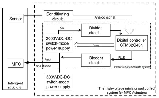
Figure 1.
Diagram of the overall control system.
Currently, the output voltage of the Discontinuous Conduction Mode (DCM) flyback DC–DC switch-mode power supply is 2000 V. Therefore, it requires regulation to produce adjustable output signals. The high-voltage power supply control system shown in Figure 1 employs an analog–digital modulation method (ADM). The fundamental principle of ADM is shown in Figure 2. The analog–digital modulation method embeds control algorithms in a digital controller. It adjusts the power stage based on the difference between the output and the desired value, eliminating steady-state error and improving steady-state performance. Compared to pure analog control, this method uses a digital controller, offering easier tuning and enabling more complex control strategies, which further optimize system performance. In contrast to pure digital control, this method adds a bleeder circuit, allowing for rapid voltage reduction.
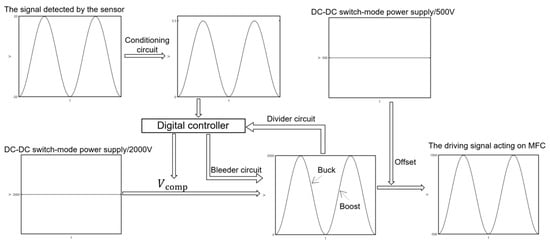
Figure 2.
Schematic diagram of the analog–digital modulation.
This method is a collaboration between analog circuits and a digital controller. The analog circuit includes a voltage divider and a bleeder circuit. The voltage divider reduces the high-voltage output from the power supply to a level within the ADC input range of the digital controller. The signal is transmitted to the digital controller and amplified in the same proportion. Therefore, this high-voltage feedback signal is compared to a reference signal in the digital controller (the reference signal represents the theoretical output of the control system). After comparison, a Type III digital compensator outputs a control signal. This control signal is sent to the PWM generator input of the DCM flyback DC-DC converter. PWM modulation regulates the duty cycle of the power stage switch, ensuring that the output signal increases in tandem with the reference signal. The reduction in the high-voltage output signal is managed by the bleeder circuit, with the digital controller controlling the bleeder circuit’s switching.
Thus, the high-voltage power supply control system can be divided into two parts: boost and buck. The collaboration between these two processes facilitates rapid and precise adjustments within the range of −500 V to 1500 V. Due to the need for asymmetric high-voltage output signals, a DC-DC converter with a 500 V output is required as an offset to achieve the desired drive voltage of −500 V to 1500 V for the MFC actuators.
2.2. Power Supply Control System
2.2.1. The Boost Section
The boost section of the high-voltage power supply control system operates as a closed-loop control system. It primarily consists of a switch signal generator, a power stage, and a controller (also known as a compensator). This is a single-input, single-output control system. is the input signal for the closed-loop system. is the output signal for the closed-loop system. Figure 3 illustrates the structure of the boost section.
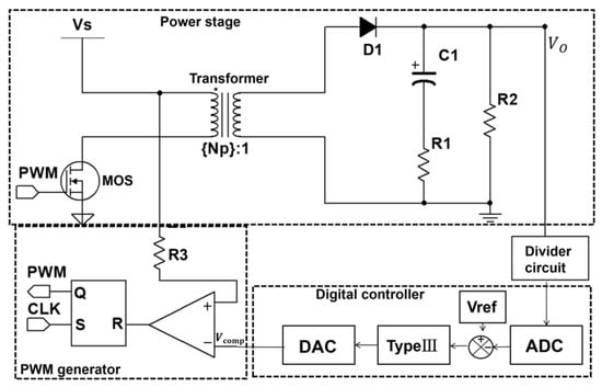
Figure 3.
Schematic diagram of the boost section.
The power stage provides voltage transformation and mainly includes MOSFET, transformer, diode, and capacitor. It employs a Discontinuous Conduction Mode (DCM) flyback architecture [13]. When the MOSFET is on, the current in the primary winding of the transformer increases, causing diode to turn off. Once the MOSFET turns off, diode conducts, allowing the secondary winding of the transformer to charge capacitor and load . When the currents in both primary and secondary windings reach zero, capacitor discharges into load .
The digital controller generates a control signal based on the difference between the actual output and the set reference value. This signal is processed through a PWM generator to produce switch signals that control the power switch in the power stage. The control signal determines the maximum current for the power stage. The timing for closing the MOSFET is controlled by a clock signal. When the MOSFET closes, the current in the transformer begins to rise. Once the current reaches the reference value set by the digital controller, the MOSFET automatically turns off, using a current-sensing resistor in the process. The PWM switching frequency is entirely determined by the clock control section, while the PWM duty cycle is dictated by the output voltage from the digital controller [14]. Due to the high switching frequency, the output voltage can rise quickly and stabilize in response to increases in the reference voltage.
Consequently, creating an accurate model is challenging. In practice, power stage modeling in switching power supplies is often based on small-signal assumptions, using linearization approximations for modeling [15].
At a specific steady-state operating point, the disturbance amplitude is much smaller than the steady-state value. The frequency is also much lower than the switching frequency. In this case, the system parameters at the steady-state operating point can be used to approximate the nonlinear relationships. Therefore, the switching frequency and its harmonics are neglected in the system loop analysis [16].
A small-signal model of a current mode DCM flyback power supply is given by [17]
In Equations (2) and (3), is the output voltage of power stage; is the output control voltage of the digital compensator; G0 is the gain of the power stage; ωz1, ωz2, and are two zeros and two poles of the power stage; Vs is the input voltage of the power stage; GFB is the small-signal gain for the power stage control system; fs is the switching frequency of the power stage; R2 is the power stage load of the power stage; is the inductance of secondary coil; is the rate of change of voltage across the sampling resistor during switching tube conduction; is an additional ramp compensation signal used to suppress subharmonic oscillations and is 0 in this power supply; R1 is the equivalent series resistance of the filter capacitor; C1 is the filter capacitor; D is the duty cycle of switching power supplies; M is the voltage transfer rate; Np is the turns ratio of the transformer.
A typical magnitude–frequency response of a power stage transfer function is shown in Figure 4. When the power stage is connected with the compensator to form a closed-loop control system, the closed-loop system’s cutoff frequency is typically much lower than . Therefore, the primary focus is on the locations of the first two or three zeros and poles in the low-frequency range, as well as the open-loop again.
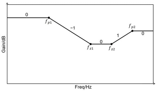
Figure 4.
The magnitude–frequency response of a power stage transfer function.
Analog compensator circuits are simple, but they have drawbacks such as inconvenient adjustment (requiring the replacement of multiple resistors and capacitors after calculations) and difficulty in implementing complex control rates. With the advancement of computer technology, digital control techniques have become widely used. By deploying the compensator model on embedded chips (e.g., STM32G431), computer numerical control systems can be realized. Digital controllers offer advantages such as ease of modification and the ability to implement complex control methods.
The role of the compensator is as follows: The power stage can be controlled based on the difference between the output and the desired value, which helps eliminate steady-state error. The compensator ensures loop stability and achieves good dynamic performance. Typically, the model of the power stage is a small-signal linearized model, and the compensator is described using a linear model in this context. A commonly used Type III controller schematic is shown in Figure 5.
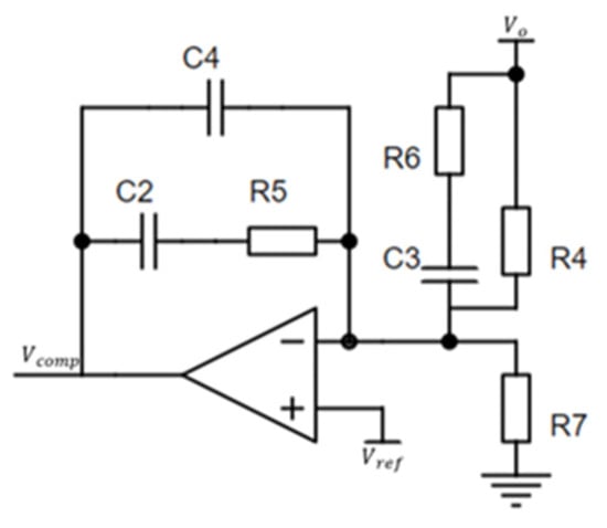
Figure 5.
Type III controller schematic.
Theorem-type environments (including propositions, lemmas, corollaries etc.) can be formatted as follows
The transfer function is:
The zero-pole expression in the transfer function is shown below.
In the field of control of power supply systems, the usual research approach is to first model and design the continuous system. Subsequently, the established continuous system model is converted into a discrete system model. A discrete control system is established with the sampling time denoted as (typically equal to the PWM switching frequency). The discrete controller has defined input and output . By applying bilinear transformation, the transfer function is converted from the continuous s-domain to the discrete z-domain, as shown below.
All coefficients are known, as follows:
The difference equation is obtained by processing Equation (6), as shown below.
Digital control systems introduce certain errors that must be corrected to function as expected with compared analog control systems. These factors include [18] the following: The delay Tc between obtaining the ADC value and the new PWM output, as shown in Figure 6. The ADC sampling process introduces a zero-order hold, resulting in a certain amount of delay, as illustrated in Figure 7. The input to the analog controller is the high-voltage power supply output, whereas the ADC input is the voltage after scaling down the high-voltage output, as depicted in the voltage divider circuit diagram in Figure 8.
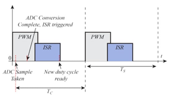
Figure 6.
The first type of delay introduced by digital controllers.
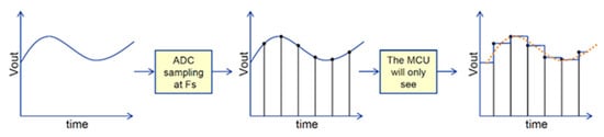
Figure 7.
The second type of delay introduced by digital controllers.
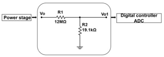
Figure 8.
Voltage divider circuit.
Adjustments must be made in the design of the digital compensator to consider these factors. The phase margin needs to be larger than that of the analog compensator to compensate for the delay. The output of the digital compensator must be scaled proportionally to correct for the scaling at the ADC input.
After addressing various details, the appropriate zero and pole locations are designed, and these parameters are stored in the microcontroller. The real-time computation of the difference equations occurs within the microprocessor. The results are then sent to the PWM generation module through the DAC. This process enables the real-time adjustment of the output voltage. The power supply system is designed with a cutoff frequency of 2 kHz and a phase margin of 55°. The optimized zero and pole parameters for the compensator are as follows:
2.2.2. The Buck Section
When a rapid reduction in output voltage is required and the control signal has already decreased to a duty cycle of zero, but the output voltage remains above the set point, the voltage drop must rely on discharge. Figure 9 illustrates the high-voltage power supply bleeder circuit. The bleeder switch is controlled by a microcontroller. Its working mechanisms are as follows: When the output voltage exceeds the reference voltage, the switch closes to enable discharge. When the output voltage is less than the reference voltage, the bleeder switch opens. Any further increase in output voltage depends solely on increasing the duty cycle. In the bleeder circuit, RLS is the control signal output by the microcontroller. A gate driver IC controls the switching states of three MOSFETs. The circuit employs six high-voltage resistors to effectively discharge the voltage, facilitating rapid voltage reduction. Additionally, diodes are incorporated into the circuit to prevent reverse current flow, ensuring the safety of the entire system.
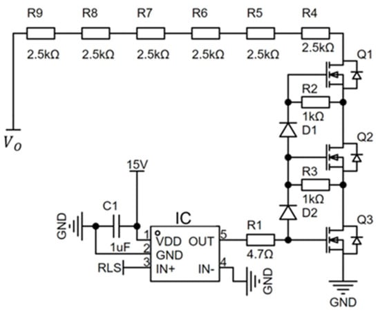
Figure 9.
Bleeder circuit.
2.3. System Software Operating Environment
This system is based on the Matlab/Simulink (2023a) software environment. The digital compensator, bleeder control, and other related codes have been developed and deployed for real-time execution on a microcontroller. All the code is integrated into the Simulink pathway, enabling the integration of the active controller and the power supply. The software environment compiles Simulink model files into binary files that can be processed by the microcontroller. It uses the STLINK-V3MINI downloader to transfer the compiled binary program to the subordinate system for execution. Additionally, this software environment facilitates communication between the host and the microcontroller, allowing it to receive control commands from the host level. This capability enables the real-time adjustment of parameters during program execution. Figure 10 shows the software operation environment based on Simulink, which enables the real-time simulation of control algorithms and the real-time recording of control and feedback signals.
Figure 10.
Simulink-based software operating environment.
3. System Characterization
3.1. Output Characteristics of High Voltage Power Supply
3.1.1. Linearity Test
Linearity describes the relationship between a system’s output and input, indicating whether it follows a linear pattern. Higher linearity correlates with greater accuracy and reliability, while lower linearity suggests larger errors within the system. A DC voltage ranging from 0 to 3.3 V was applied to the input of the control system, with a scan increment of 0.005 V. The resulting linearity curve between the input and output is shown in Figure 11. The figure demonstrates that the driving system exhibits excellent linearity within its rated range. When the magnification is constant and the input voltage is different, the output voltage is proportional to the input voltage, which shows that the system has a high linearity. Compared to the existing design, it improves its linearity by adding a digital compensator.
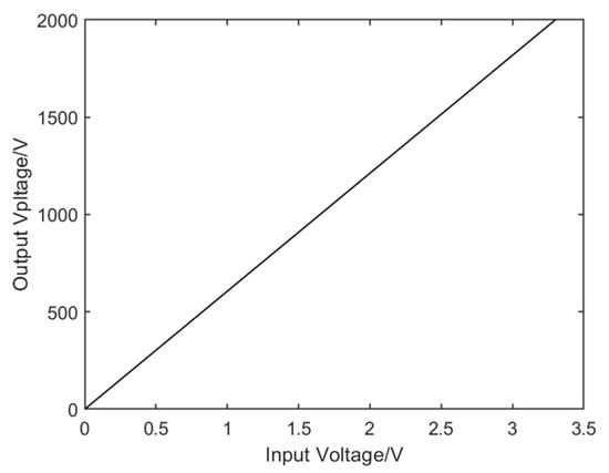
Figure 11.
System linearity test curve.
3.1.2. Step Response Test
By analyzing and verifying the response of the high-voltage power supply to step signals, we can evaluate whether its design meets the specified requirements. In the step response test, the load of the high-voltage power supply was set to 474 nF, with an output period of 1 s and a peak voltage of 2000 V. A square wave signal was used with a sampling frequency of 1000 Hz. As shown in Figure 12, the test results illustrate the high-voltage power supply’s response to the square wave signal. The results indicate that the power supply exhibits good dynamic response during load driving. The control circuit’s output voltage smoothly rises from 0 V to 2000 V, displaying minimal overshoot upon reaching 2000 V. This demonstrates a high level of stability, which aligns with the design requirements of the power supply.
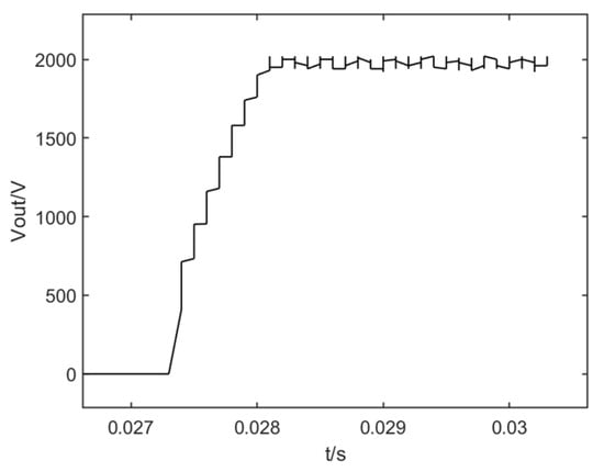
Figure 12.
High voltage drive power supply step response curve.
3.1.3. Dynamic Response Test
Observing the output sine wave response of the high-voltage power supply by inputting a simulated sine wave voltage signal is an important method for evaluating its output response. The frequency characteristics of the high-voltage power supply were tested at output voltages ranging from −500 V to 1500 V with different loads to assess performance. High-voltage capacitors with capacitance values of 104 nF, 154 nF, 224 nF, and 474 nF were selected as the equivalent load for the MFC.
Figure 13 illustrates the power bandwidth curve under maximum output power conditions. The analysis indicates that, with increasing frequency, the peak-to-peak voltage output of the high-voltage controller shows a slight upward trend, followed by a gradual decline. This phenomenon may be attributed to the use of small-signal modeling in the power stage, making it challenging to establish an accurate system model. This, in turn, affects the precision of the control section of the high-voltage controller. By selecting peaks in the amplitude–frequency characteristic curve for error calculation, the results show that the errors are small and have minimal impact on the driving of the MFC.
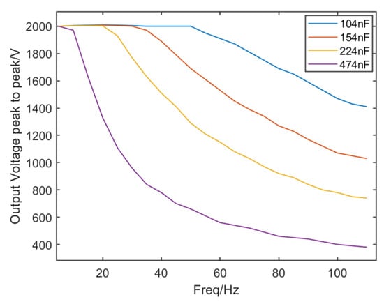
Figure 13.
High voltage power supply bandwidth curve.
Further examination of the figure reveals that, at output voltages ranging from −500 V to 1500 V, the bandwidth is 40 Hz for a load capacitance of 104 nF, 25 Hz for 154 nF, 15 Hz for 224 nF, and 5 Hz for 474 nF. Additionally, the test results for the load bandwidth of the high-voltage power supply at different output voltages are shown in Table 1. Since the power stage is fixed at 40 W, the bandwidth at the same load increases as the output voltage decreases.

Table 1.
Load bandwidth at different output voltages.
Figure 14 presents a comparison of the input and output waveforms of the high-voltage power supply. In Figure 14a, the waveform is shown with a load of 104 nF at a frequency of 40 Hz. Figure 14b illustrates the waveform with a load of 154 nF at a frequency of 25 Hz. Figure 14c displays the waveform with a load of 224 nF at a frequency of 15 Hz. Finally, Figure 14d shows the waveform with a load of 474 nF at a frequency of 5 Hz. The test results indicate that there is no phase shift in the output waveforms. The dynamic response is satisfactory, and the waveforms are smooth. These observations suggest that the power supply has the ability to drive loads rapidly and effectively.
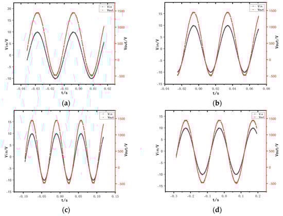
Figure 14.
Comparison of input and output waveforms of high voltage power supplies; (a) load is 104 nF and frequency is 40 Hz; (b) load is 154 nF and frequency is 25 Hz; (c) load is 224 nF and frequency is 15 Hz; (d) load is 447 nF and frequency is 5 Hz.
3.2. System Parameter
By testing various performance indicators of the high-voltage miniaturized control system (as shown in Figure 15), we obtained the corresponding system parameters, detailed in Table 2. By comparing the performance indicators with those of the piezoelectric actuator in the literature, it can be seen that all the performance indicators of this control system have met the design requirements. According to the data presented in Table 2, the designed high-voltage miniaturized control system can output asymmetric driving voltages. It exhibits good dynamic response performance, high load capacity, and significant power output. Additionally, it demonstrates advantages in terms of size and weight.
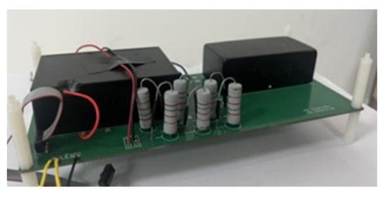
Figure 15.
Photo of the practical controller.
Table 2.
High-voltage miniaturized control system parameters.
4. Experimental Validation and Analysis
The study of vibration suppression in high-aspect-ratio wings is of significant importance for the longevity of long-duration high-altitude flights [19]. Active control using Macro Fiber Composites (MFC) actuators is an effective method for damping vibrations in high-aspect-ratio wings. As illustrated in Figure 16, the experimental rig is dedicated to active control experiments on airfoil and features a newly designed high-voltage miniaturized control and system.
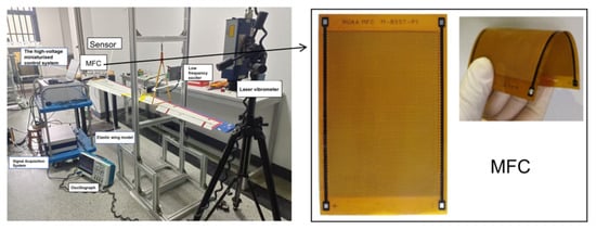
Figure 16.
Wing active control experiment rig.
MFC actuators are affixed to the root of the flexible wing. Piezoelectric ceramics serve as displacement sensors to collect the wing’s displacement signals. An exciter applies stimulation at the first bending natural frequency of the wing’s composite structure. This approach aims to achieve maximum vibrational displacement of the wing. Additionally, a laser vibrometer is used to measure displacement changes before and after vibration control. When using a laser vibrometer to measure the vibration displacement of a wing, the laser is first calibrated, then the output port is connected to an oscilloscope and the appropriate range is selected.
The frequency domain HHC algorithm [20] combined with the miniaturized high-voltage control system is used to carry out active control experiments on the wing. The results of the experiments are shown in Figure 17 below, which shows the real-time variation of the wing end displacement. It can be seen that about 5 s ago, the vibration displacement of the wing end decreased significantly, and the control speed was faster.
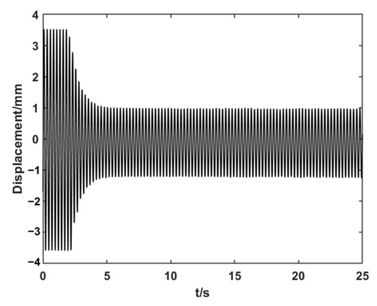
Figure 17.
Active control process.
Figure 18 shows the wingtip displacement images before and after control. The left image depicts the displacement curve within 1 s at the start of the experiment before active control was applied, while the right image shows the displacement curve within 1 s after the system reached a steady state with active control. It can be observed that, compared to the pre-control conditions, the vibration displacement at the wingtip was reduced by 65% after active control was implemented. The output voltage of the high-voltage control system after the control reached steady state is shown in Figure 19, and the output voltage was −166 V to 322 V.
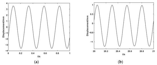
Figure 18.
Displacement images of the wing ends; (a) displacement before control; (b) displacement after control.
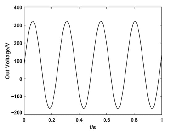
Figure 19.
Output voltage curve.
Therefore, the high-voltage miniaturized control system designed in this paper incorporates an active control algorithm for experimental validation. The results demonstrate a good control performance, indicating the effectiveness of this system for use in active control experiments.
5. Conclusions
This paper proposes a regulation method for a discontinuous conduction-mode flyback switch-mode power supply operating in current mode. This method employs a mixed analog–digital modulation method, enabling adjustable voltage outputs ranging from −500 V to 1500 V. Based on this hybrid control approach, we have designed a high-voltage miniaturized control system for MFC drivers. This system addresses the high-voltage driving requirements of MFCs while meeting the demand for compact control systems. Further, the control system features dynamic response capabilities, high load capacity, and substantial power output. It is integrated with a Simulink-based software environment, allowing for real-time adjustment and the simulation of active control algorithms. In verification experiments for vibration reduction with a large aspect ratio, the application of this control system achieved a vibration reduction effect of 65%. Additionally, the high-voltage signals output by the system were stable. However, there remains potential for optimizing its power bandwidth. The power stage bandwidth can be improved by optimizing the digital compensator, e.g., by implementing adaptive changes in the digital compensator algorithm for different drive voltages and for different loads. Therefore, further research on this system holds significant academic value and practical significance.
Author Contributions
Conceptualization, Z.L. and H.J.; data curation, Z.L.; investigation, Z.L., Y.W., C.Z. and C.T.; methodology, Z.L., H.J. and Y.W.; resources H.J. and J.Q.; software, Z.L.; validation, Z.L. and Y.W.; visualization, Z.L.; writing—original draft, Z.L. and H.J.; writing—review and editing, Z.L., H.J. and Y.W. All authors have read and agreed to the published version of the manuscript.
Funding
This work is supported by the National Key Research and Development Program of China (Grant No. 2021YFB3400100), National Natural Science Foundation of China, Grant/Award Numbers: 52241103, U2241261.
Data Availability Statement
The data that support the findings of this study are available from the corresponding author upon reasonable request.
Conflicts of Interest
The authors declare no conflicts of interest.
References
- Wu, Y.; Yuan, Q.; Ren, K.; Shen, X.; Shen, H.; Badel, A.; Ji, H.; Qiu, J. Bidirectional energy-controlled piezoelectric shunt damping technology and its vibration attenuation performance. Int. J. Mech. Syst. Dyn. 2024, 4, 63–76. [Google Scholar] [CrossRef]
- Lin, X.-J.; Zhou, K.-C.; Zhang, X.-Y.; Zhang, D. Development, modeling and application of piezoelectric fiber composites. Trans. Nonferrous Met. Soc. China 2013, 23, 98–107. [Google Scholar] [CrossRef]
- Guo, Y.; Yu, Y.; Li, L.; Zhang, D.; Liao, W.-H.; Du, C.; Guo, X. Modeling and vibration control of a rotating flexible plate actuated by MFC. Compos. Struct. 2024, 331, 117907. [Google Scholar] [CrossRef]
- Li, C.; Shen, L.; Shao, J.; Fang, J. Simulation and experiment of active vibration control based on flexible piezoelectric MFC composed of PZT and PI layer. Polymers 2023, 15, 1819. [Google Scholar] [CrossRef] [PubMed]
- Zhou, J.; Zhou, J.; Chen, W.; Tian, J.; Shen, J.; Zhang, P. Macro fiber composite-based active and efficient suppression of low-frequency vibration of thin-walled composite beam. Compos. Struct. 2022, 299, 116019. [Google Scholar] [CrossRef]
- Luo, Y.; Yang, F.; Ji, L.; Zhang, Y.; Xu, M.; Zhang, X. Research on active vibration control of flexible wing based on MFC actuator. Int. J. Appl. Electromagn. Mech. 2020, 64, 565–571. [Google Scholar] [CrossRef]
- Gao, Z.; Huang, J.; Miao, Z.; Zhu, X. Multiple model switching adaptive control for vibration control of cantilever beam with varying load using MFC actuators and sensors. Smart Struct. Syst. 2020, 25, 559–567. [Google Scholar]
- Tung, Y.C.; Jeng, S.L.; Chieng, W.H. Multi-level balanced isolated floating difference amplifier. IEEE Trans. Circuits Syst. I Regul. Pap. 2008, 55, 3016–3022. [Google Scholar] [CrossRef]
- Milecki, A.; Regulski, R. Investigations of electronic amplifiers supplying a piezobimorph actuator. Mech. Syst. Signal Process. 2016, 78, 43–54. [Google Scholar] [CrossRef]
- Zhang, D.; Zhong, B.; Jin, Z.; Wang, Z.; Sun, L. High-voltage amplifier with high dynamic response for stick–slip driving. Circuits Syst. Signal Process. 2020, 39, 2759–2775. [Google Scholar] [CrossRef]
- Xu, L.; Li, H.; Li, P.; Ge, C. A high-voltage and low-noise power amplifier for driving piezoelectric stack actuators. Sensors 2020, 20, 6528. [Google Scholar] [CrossRef] [PubMed]
- Pisenti, N.C.; Restelli, A.; Reschovsky, B.J.; Barker, D.S.; Campbell, G.K. An ultra-low noise, high-voltage piezo-driver. Rev. Sci. Instrum. 2016, 87, 124702. [Google Scholar] [CrossRef] [PubMed]
- Jing, Z.; Shuang, W.H.; Jun, R.X.; Ya, Z.L. Design of a flyback high-efficiency switching power supply. J. Phys. Conf. Ser. 2021, 1748, 052042. [Google Scholar] [CrossRef]
- Hung, C.W.; Liang, J.M.; Hsu, W.T.; Yang, C.C. A design of flyback switched-mode power supply with softswitching using the UC3842 controller. J. Phys. Conf. Ser. 2021, 2020, 012031. [Google Scholar] [CrossRef]
- Feng, W.; Chen, Y.; Jiang, J.; Jiang, W. Modeling and controller design of flyback converter operating in DCM for LED constant current drive. IOP Conf. Ser. Earth Environ. Sci. 2020, 512, 012172. [Google Scholar] [CrossRef]
- Basso, C. Switch-Mode Power Supplies: SPICE Simulations and Practical Designs; The McGraw-Hill Companies, Inc.: New York, NY, USA, 2008. [Google Scholar]
- Tajuddin, M.F.N.; Rahim, N.A.; Daut, I.; Ismail, B.; Mohammed, M.F. State space averaging technique of power converter with digital PID controller. In Proceedings of theTENCON 2009–2009 IEEE Region 10 Conference, Singapore, 23–26 January 2009. [Google Scholar]
- Hallworth, M.; Shirsavar, S.A. Microcontroller-based peak current mode control using digital slope compensation. IEEE Trans. Power Electron. 2012, 27, 3340–3351. [Google Scholar] [CrossRef]
- Brown, J.D.; Mustafa, M.; Moore, K.J. Vibration mitigation of a model aircraft with high-aspect-ratio wings using two-dimensional nonlinear vibration absorbers. Int. J. Non-Linear Mech. 2024, 167, 104878. [Google Scholar] [CrossRef]
- Beaumier, P.; Prieur, J.; Rahier, G.; Demargne, A.; Tung, C.; Gallman, J.M.; Yu, Y.H.; Kube, R.; van der Wall, B.G.; Schultz, K.J.; et al. Effect of higher harmonic control on helicopter rotor blade—Vortex interaction noise: Prediction and initial validation. In Proceedings of the 75th Fluid Dynamics Panel Symposium on Aerodynamics and Aeroacoustics of Rotorcraft, Berlin, Germany, 10–13 October 1994. [Google Scholar]
Disclaimer/Publisher’s Note: The statements, opinions and data contained in all publications are solely those of the individual author(s) and contributor(s) and not of MDPI and/or the editor(s). MDPI and/or the editor(s) disclaim responsibility for any injury to people or property resulting from any ideas, methods, instructions or products referred to in the content. |
© 2024 by the authors. Licensee MDPI, Basel, Switzerland. This article is an open access article distributed under the terms and conditions of the Creative Commons Attribution (CC BY) license (https://creativecommons.org/licenses/by/4.0/).