1. Introduction
Over the last fifteen years, in many fields a rapid growth of microfluidic device applications has been observed [
1]. Most of them are applied in medicine (chemical and microbiological analyses), drug discovery and production (fine and uniform in size droplets or particles formation, meds encapsulation
etc.), biotechnology (bioreactors and cells characterization) and ecology (analytical and microbial purposes).
Simpler microfluidic devices can be easily controlled by pressure or fluid flow rates [
2]. However, externally driven valves, pumps, switches and flow regulators are used in more advanced systems [
3]. Devices controlled in a pneumatic [
4], electromechanic [
5] or mixed [
6] way operate up to 100 Hz. Faster operation (up to 6 kHz) can be performed utilizing piezoceramic elements working as actuators in flow and other parameter controlling devices [
7]. It is noteworthy that despite such an attractive opportunity, most microfluidic valves [
8,
9] and pumps [
10,
11] operate with frequency lower than 1 kHz. The reason is that maximal operating frequency is limited due to inertia force acting on liquid accelerated and decelerated in channels and hoses supplying microfluidic device and preventing variation of flow direction.
The other equipment applied in microfluidic devices: separators for solid particles removal [
12], liquid dispensers [
13], cell sorters [
14]
etc., usually operate with frequencies up to about 2.5 kHz.
Piezoceramic actuators used in microfluidic devices are typically controlled with square electric waves. Applied voltages do not exceed 400 V and in most cases variation of the signal between 0 and ca. 200 V is sufficient. Considering the relatively elevated pricing of linear drivers and the fact that typical automated microfluidic systems use multiple valves, the cost of the generators can contribute a significant portion of the investment into the setup. Since there is a progressive demand for point-of-care, or generally, off-site testing with the use of microfluidic systems there is the associated important challenge of constructing inexpensive drivers for high-speed microvalves.
In microfluidic applications involving generation of droplets on demand crucial parameters include the intervals needed by the system to react to the signal by either closing or opening the valve. Square wave signals are used for driving piezoceramic actuators in pumping applications [
15,
16,
17] and in valveless devices [
18,
19]. It is experimentally proven that piezoelectric pumps driven by square waves achieve better characteristics than those driven with sine waves [
15]. Short intervals needed either for complete opening for flow or for complete closure allow maximization of the operation frequency of the system.
2. The Aim
Microfluidic applications demand affordable drivers for piezoceramic valves, characterized by relatively large (above 1 μF) capacity. The typical requirements of linearity of gain and of low level of distortions are less important than the requirement of rapid amplification of square wave input signal (0–10 V) into approximately rectangular output signal (0 up to 150–180 V).
3. The Circuit
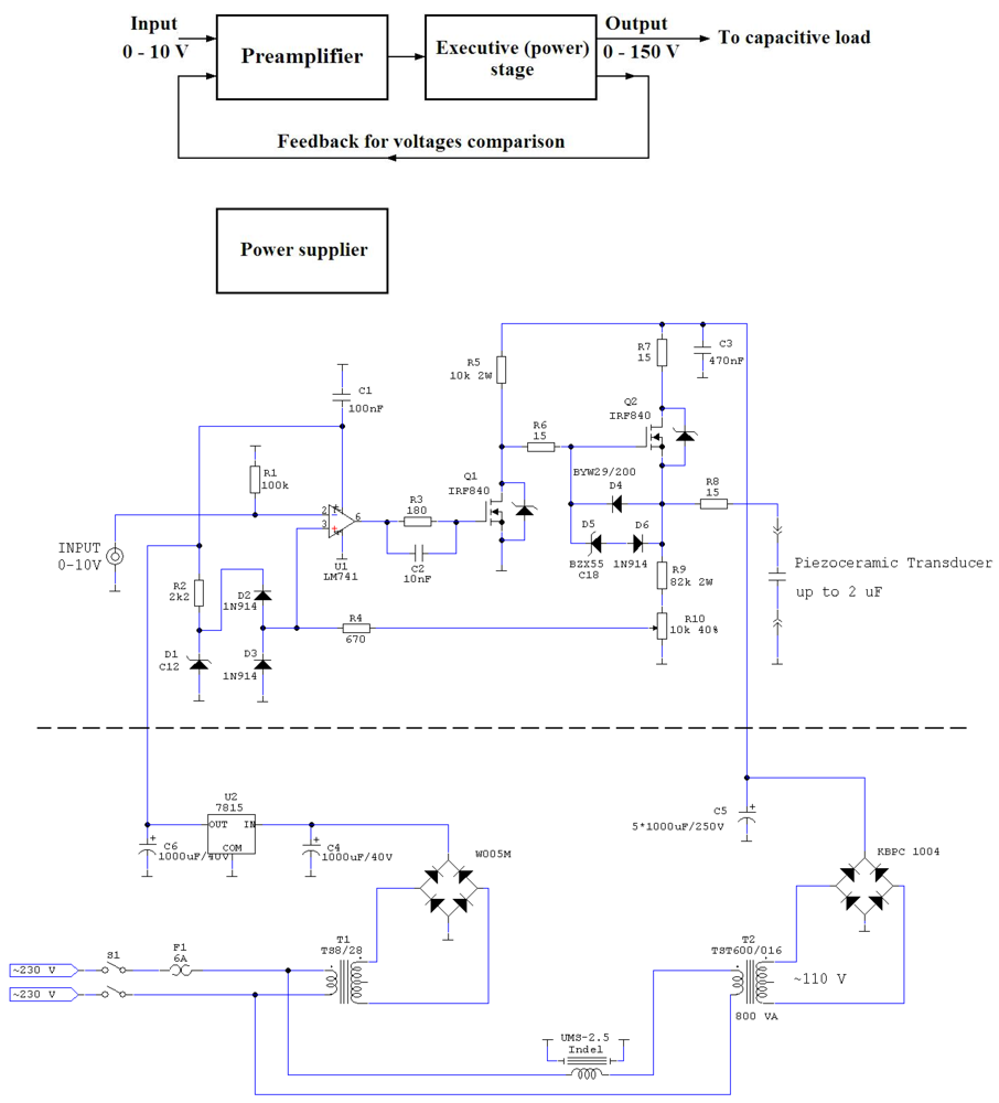
The driver comprises a preamplifier, a set of executive power transistors and a power supply. The scheme of the device is shown in
Figure 1. The preamplifier is built on an operational amplifier of U1 (LM741) with an open feedback loop that yields maximal allowable bandwidth (up to 30 kHz). Its inverting input can be supplied from commonly available external sources that are capable of supplying high opening (e.g., 10 V) and low closing (e.g., 0 V) levels of input voltage. Applied driving signal should be formed as a square wave with as short as possible rising and falling times.
Application of the high level input (10 V) results in a decrease of voltage at the gate of Q1 (IRF840) CMOS transistor. Consequently, gate capacity of Q2 (IRF840) starts loading by resistors R5, R6 and then its gate voltage increases. This results in loading of the transducer capacity via transistor Q2 and resistors R7 and R8. These resistors limit the loading current to 5 A. Charging characteristics of the gate capacity of Q2 and of the transducer capacity are adjusted in such a way as to sustain the gate-source voltage of Q2 at a safe level (less than 30 V) [
20,
21]. This is possible for transducer capacities less than 3 μF. For larger capacities of the transducer it is necessary to protect the gate of Q2 against its break-down by excessive voltage with the use of diodes D5, D6. The small current flowing through the R9 resistor (82 kΩ) and through the potentiometer R10 (10 kΩ) to the ground generates a small voltage drop introduced via R4 (670 Ω) to non-inverting input of U1. The circuit formed by R2, D1, D2 and D3 keeps the voltage level applied to the non-inverting input of U1 at a safe level limited to the range of approximately 0–12.6 V.
Figure 1.
The circuit diagram divided into specific functional groups (upper panel). Schematic of single channel of the driver and power supply (lower panel).
Figure 1.
The circuit diagram divided into specific functional groups (upper panel). Schematic of single channel of the driver and power supply (lower panel).
Decrease of signal at the input of the driver results in an increase of voltage at the gate of Q1—opening this transistor. Then the voltage at the gate of Q2 drops below the level at its source. This switches Q2 to the closed state and begins the process of discharging of the piezoceramic capacitor through R8 (15 Ω), the diode D4 (BYW29/200), R6 (15 Ω) and the transistor Q1. The circuit comprising C2 and R3 is responsible for the decrease of the charging- and discharging-times of the gate-source capacity of Q1. This in turn leads to a decrease of the time of falling and rising of the signal (i.e., increases the fidelity of amplification of the signal at the edges of the on/off intervals).
We note here that the driver that we describe operates similarly to a voltage comparator. The piezoceramic capacitor is being charged (or discharged) until the voltages at inverting- and non-inverting inputs of U1 differ. Due to the high level of gain at U1 and to the relatively large capacity of the piezoceramic actuator the fluctuations of the output voltage are negligibly small (amplitude of fluctuations, ca. 1% of the peak voltage). Even at zero load capacity (i.e., when the transducer is disconnected) these fluctuations are still small due to the CMOS gate-source capacities and other capacities present in the circuit.
Typically, microfluidic experiments demand the use of a number of piezoceramic actuators at the same time. Thus, in many applications it will be preferred to have several driver lines in a single housing. We placed four drivers in a single case with one common power supply. We used the economical 8 W transformer T1 (TS8/28), typical rectifier W005M, electrolytic capacitor C4 (1,000 µF/40 V) and the U2 (7815) voltage regulator for the low voltage power supply. The high voltage supplier has a much greater power comprising a 600 W transformer T2 (TST600/016), high current rectifier KBPC 1004 and five 1,000 µF/250 V (C5) capacitors. For synchronous operation of four drivers (in a box) a more powerful transformer and a bigger number of electrolytic capacitors should be used. It should be stressed that in the case of large transformers a special circuit UMS-2.5 (Indel) limiting startup current has to be applied. Without this precaution, the act of switching on the power may result in blowing the fuses.
4. Construction and Setup
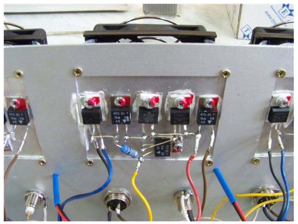
The power dissipated by the driver is directly proportional to the frequency of the square wave signal–or more generally, for non-periodic signals, to the number of rising and falling edges per second. The modules that release most of the heat (Q1, Q2, D4, R6-8) thus need to be connected to a heat sink (
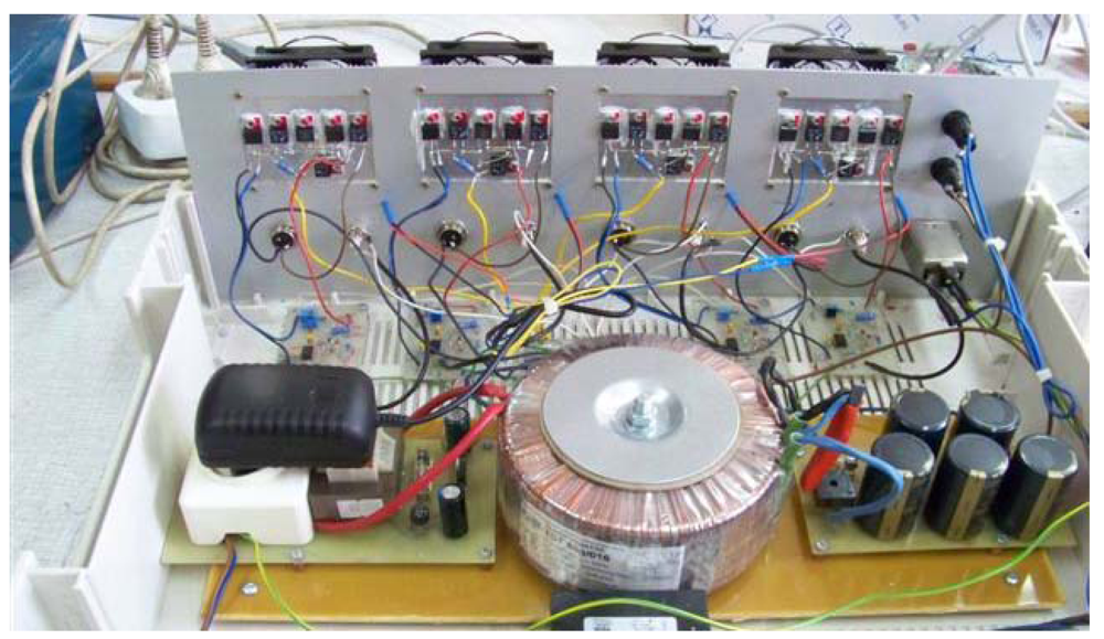
Figure 2). In our design every driver channel is equipped with a separate, fanned, heat sink. Importantly, correct operation of the driver requires that the resistors R6-8 are non-inductive and that the power dissipated in them exceeds 50 W. Conveniently such resistors are accessible in TO-220 packages. High voltage rectifier should be screwed to the chassis to prevent its overheating. The other electronic elements can be mounted on universal printed boards (
Figure 3). Commercial power supply (12 V) can be used for fans that cool the heat sinks.
A properly soldered circuit should start proper operation immediately after being switched on. The only parameter that must be adjusted is the maximum voltage that can be applied to the piezoceramic transducer. This can be done by adjusting the potentiometer R10 while a 10 V constant signal is applied to the driver input.
Figure 2.
The heat sink with the resistors.
Figure 2.
The heat sink with the resistors.
Figure 3.
Internal view of the 4-channel driver.
Figure 3.
Internal view of the 4-channel driver.
5. Test Results
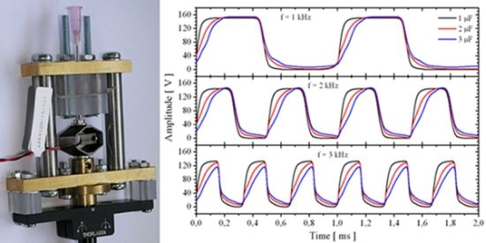
Usually manufacturers of the piezoelectric actuators specify their capacity. Thus, the operation of the driver can be easily simulated by attaching a proper capacitor to the driver output. Due to the limitations in the output current the shape of the output signal becomes more and more trapezoidal for increasing capacity of the actuator (
Figure 4). Recordings of the shape of the signal allow decision as to whether the resolution of the edges is acceptable for a particular microfluidic application.
Figure 4.
The output signal with a capacitive load (transducer) of 1, 2 and 3 μF (150 Vp-p, for 1, 2 and 3 kHz) connected to the driver.
Figure 4.
The output signal with a capacitive load (transducer) of 1, 2 and 3 μF (150 Vp-p, for 1, 2 and 3 kHz) connected to the driver.
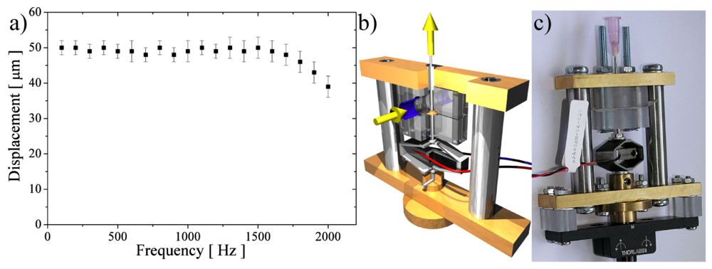
The dependence of the linear displacement of a real APA40SM (capacity of 1.8 μF) piezoelectric actuator (Cedrat,
http://www.cedrat.com) on the frequency of the signal is shown in
Figure 5. The actuator has a capacity of 1.8 µF. The mark space ratio equals one,
i.e., it is divided into equal intervals of high and low level. The test was performed for unloaded actuator
i.e., without any attached mechanical elements. The results show that the linear expansion of the actuator is almost constant up to 1,700 Hz and then the amplitude of motion decreases with increasing frequency.
Figure 5.
(a) Measured displacement of the loaded APA40SM actuator versus the frequency of the driving signal (150 Vp-p); (b) The piezoelectric valve scheme (the arrows show fluid inlet and outlet); (c) The real piezoelectric valve constructed in our microfluidic laboratory.
Figure 5.
(a) Measured displacement of the loaded APA40SM actuator versus the frequency of the driving signal (150 Vp-p); (b) The piezoelectric valve scheme (the arrows show fluid inlet and outlet); (c) The real piezoelectric valve constructed in our microfluidic laboratory.
6. Potential Limitations in Further Improvement of the System
In microfluidics it is rather rare that frequencies in excess of 1 kHz are used to drive piezoceramic actuators. Apart from electro-mechanical limitations, the very properties of liquids and physics of flow (inertia, elastic compliance etc.) often limit higher-frequencies of driving. Nonetheless there are applications (in e.g., sorting, or high-speed formation of droplets) that could benefit from the availability of higher frequencies of forcing. Below we propose a list of potential improvements in the design that we presented above that could aid in achieving even higher frequencies of driving the piezoelectric actuator.
First of all, a further increase of the frequency of the driver demands further shortening of the rise- and fall- intervals of the amplified signal. In other words, the maximum current handled by the transistors Q1 and Q2 needs to be increased. Consequently, the power dissipated by them would be increased. Unfortunately, typically, the specifications of common transistors list only the maximum power (maximum drain current) for a single square pulse. The only additional parameters available refer to the heat transfer between the transistor package and the heat sink. In our circuit the most important parameter for safe and reliable operation of the driver is the rate of the heat transfer between the semiconductor structure and the surrounding package (i.e., within the integrated block containing the transistor). In other words, it is possible that while the housing of the transistor remains relatively cool, the semiconductor structure inside is already heated up to temperatures that endanger its operation. Similar limitation occurs for the D4 diode. Fortunately, diodes are more often specified with the maximum forward current which facilitates the design of circuits similar to the one presented above.
The values of the resistance of resistors R6-8 need to be adjusted to the demanded maximum charging and discharging currents and to their maximum dissipated power. It should be stressed that each of these resistors has to be characterized by the real resistance (i.e., without the inductive component). Designs based on the complex resistance may produce significantly distorted output signals.
Finally the integrated circuit applied as preamplifier can be replaced by “faster” unit i.e., LF355.
7. Conclusions
The driver that we presented above operates properly with capacitive loads of up to about 3 µF, frequency of 1 kHz and maximum output voltage variation of 0–150 V. Decrease of piezoelement capacity leads to shortening of the intervals needed to rise (or fall) the output signal, i.e., to higher fidelities of amplifying the edges of the signal. The driver accepts a 0–10 V square wave signal at the input to reach full voltage variability range at the output.
The circuit can be easily improved for an increase of the charging and discharging current and increase of maximal output voltage. However, due to limited information published in power transistor datasheets their experimental adjustment concerning heat dissipation has to be done. This limits the potential for improvement of the parameters of the driver mostly to the replacement of the power CMOS transistors. Other elements, operating with larger current (like D4) or dissipating larger power (like R6-8) can be easily found via proper selection.
