1. Introduction
The phenomenon of negative temperature coefficient of resistivity (TCR)
< 0 in disordered metals [
1], found from temperature variation of their dc transport,
, was considered and qualitatively evaluated by many researchers [
2,
3,
4,
5,
6,
7] in terms of weak localization effect [
8]. Generally, a weak localization interference effect takes place under the assumption that the electron wavelength is much smaller than the mean free electron path. At that point, the temperature is so low that the times of all inelastic processes
, including electron-electron and/or electron-phonon scattering, during which the electron wave function coherence is preserved, are much longer than the elastic collision time
. In this case, interference effects for the electron trajectories with self-intersection lead to the increased scattering probability, i.e., to the increased resistivity, which was estimated in the first approximation of perturbation theory [
8,
9]. The diffusional character of electronic motion in a medium with impurities is generally satisfied at very low temperatures, in the regime of residual resistance. In principle, under the condition of increased disorder, scattering by static structural defects may occur more frequently than inelastic scattering by phonons in the appropriate temperature range. This condition may be fulfilled in high-resistivity alloys, where the mean free path of conduction electrons in the process of elastic scattering at the static defects is of the order of magnitude of interatomic distance
~
a ~
(where
~
is the Fermi wavenumber). It was proposed that, due to this condition, weak localization correction may take place in disordered metals and determine non-metallic character of their dc transport and negative TCR till room temperature [
5,
6,
7].
However, as a rule, the weak localization correction is small. Additionally, one-particle Anderson localization is expected in disordered metals under conditions of strong disorder. As a result, discrete localized electronic states appear near the Fermi level. One might expect the effect of fortifying electron correlations between the localized electrons. Thus, the interplay of disorder and electron correlations can lead to subtle many-body effects in localizing electrons, which represent fundamental challenges. These effects could be in evidence at optical frequencies. Here we propose an investigation of the dc transport of
-Ta films having large negative TCR [
10] in relation to their optical conductivity properties for various degrees of disorder. For that, we suggest to use a spectroscopic ellipsometry approach, which was successfully applied in our earlier studies of electronic correlations in Mott-Hubbard insulators [
11,
12,
13] and localization effects in the Kondo-lattice metal Ta
PdSi
[
14].
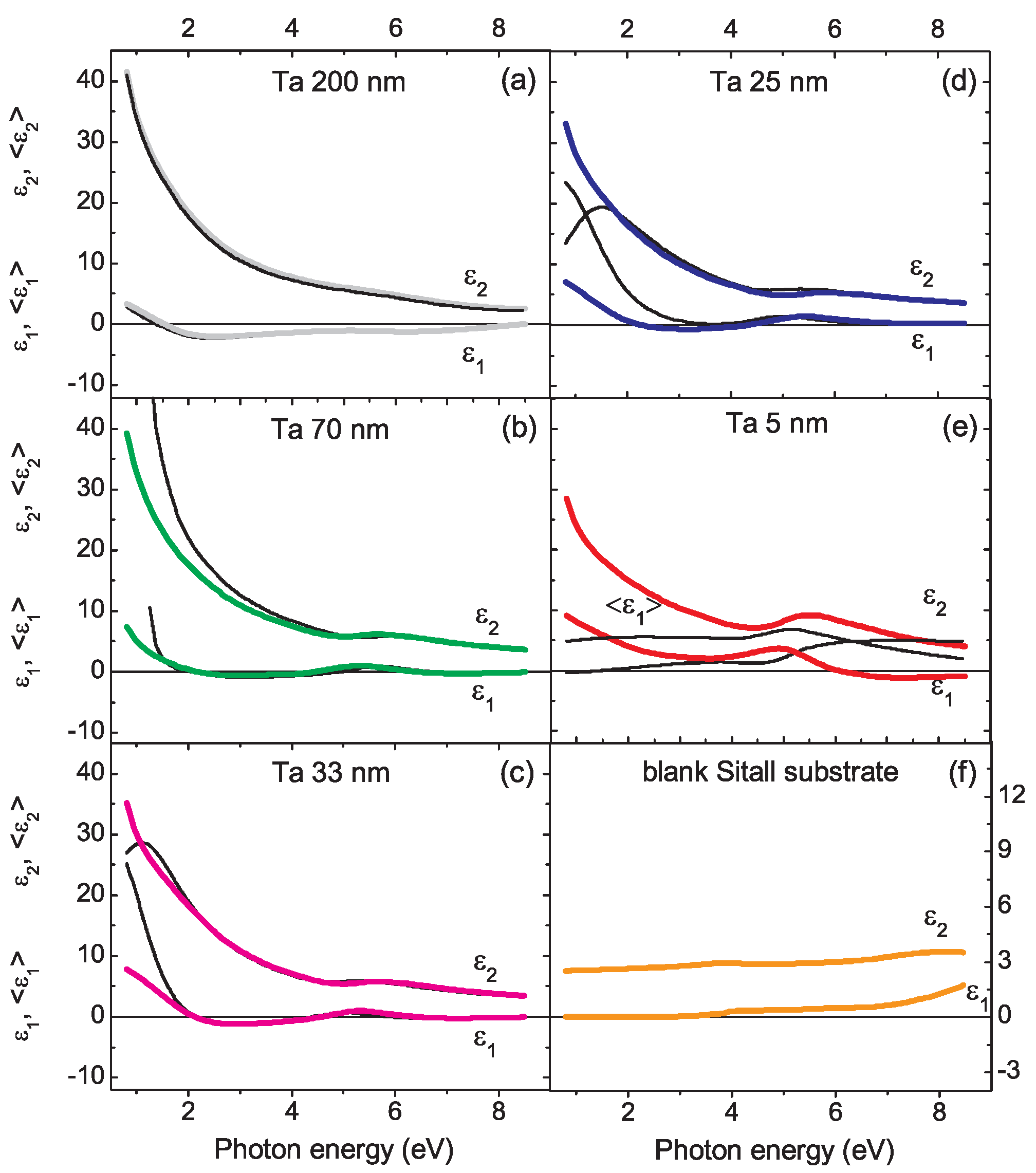
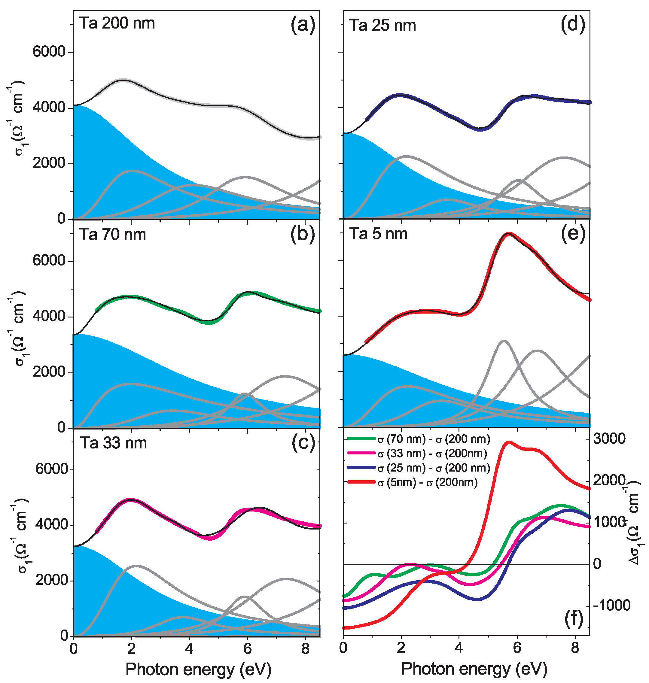
In the present study, -Ta films, grown by rf sputtering deposition on a glass Sitall substrate, were investigated by four-point probe dc transport method and by spectroscopic ellipsometry with a J.A. Woollam VUV-Gen II spectroscopic ellipsometer. The dc transport study of the -Ta films implies non-metallic behavior ( < 0) with large negative TCR values. In addition, our ellipsometry study demonstrates that the real part of the complex dielectric function of the studied -Ta films shows the peculiar non-metallic behavior. We found that the observed non-metallic behavior is due to the presence of the pronounced Lorentz band around 2 eV, which is strongly superimposed with the free charge carrier Drude response at low photon energies. In addition, we found that with increasing degree of disorder in the -Ta films, as indicated by increasing absolute value of their TCR, the Drude contribution decreases, implying the enhanced charge carrier localization, and the intensity of the Lorentz band around 2 eV increases. Moreover, we found that the pronounced changes occur at the extended spectral range, involving also the higher-energy Lorentz bands. We suggest that this is indicative of the attendant electronic correlations in highly disordered metals due to many-body effects.
The results of the present study can be useful in comprehension of many-body effects in mixed-valent magnetic compounds A
B
Mn
Mn
O
with A–B structural disorder, as well as in superconducting iron-based layered oxypnictides LaFeAsO
F
with O–F structural disorder, and other doped compounds of strongly correlated electron systems, on the basis of electronic localization due to structural disorder [
15,
16,
17].
2. Materials and Methods
Ta films were grown by rf sputtering deposition from 99.95% pure Ta target on a glass substrate Sitall, commonly used for film substrates in microelectronics. In the process of preparation for rf sputtering, the vacuum chamber was subjected to annealing at the temperature 200
C during one hour. The chamber base pressure before beginning the rf sputtering was about 2 × 10
Torr. In the present rf sputtering experiments, a background Ar pressure was 6 × 10
Torr, and the actual substrate temperature was about 80
C only. In our experiments we used the substrates with typical sizes of 15 × 5 × 0.6 mm
. The film thickness was estimated by the deposition time, at which the material deposition rate was determined according to the procedure described in detail in Ref. [
18]. A set of the Ta films with different thickness was prepared. Usually, microstructure of the thin films grown by rf sputtering is thickness-dependent. Indeed, one would expect that elevation of the film surface temperature caused by rf discharge, as well as local surface heating caused by atom bombardment with high energy of about 1 eV, leads to the annealing effect and grain growth along the film profile. Therefore, it is expected that the thinner Ta films, grown in the present study at the same rf sputtering conditions, will possess higher degree of disorder. By contrast, we suppose that concentration of oxygen defects, which can be caused by oxygen presence at a background level of 10
–10
mbar in using Ar gas, will be much less thickness dependent, as its absorption occurs permanently in the process of film growing. To protect from oxidation, the as deposited Ta films were capped in situ with Al
O
layer of 2.1 nm thick. The Al
O
capping layer was prepared by rf sputtering of a single-crystal sapphire target. Our earlier studies [
19,
20] show that even monolayers of active metals covered by the 2.1 nm Al
O
capping layer did not change their electronic properties during at least several years.
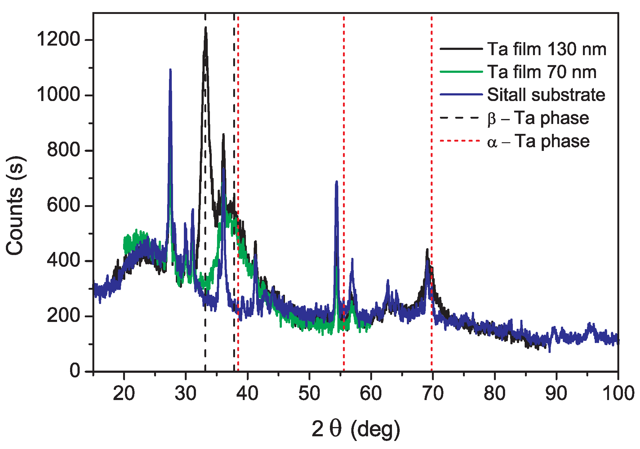
A phase and a crystal structure of the sputtered Ta films were characterized by X-ray diffraction (XRD) analysis using Panalytical X’pert Pro MRD Extended Diffractometer (PANalytical, Almelo, The Netherlands) operating at 40 kV and 30 mA with Cu K
radiation. The
-
scans ranged between 15
and 100
with a step size of 0.02
and with time per step of 0.2 s were obtained.
Figure 1 shows the XRD spectrum of the blank Sitall substrate. The analysis of the XRD diffraction pattern showed that it is represented by the TiO
rutile phase. In
Figure 1 the XRD spectrum of the Ta film of 130 nm thick is superimposed with the XRD spectrum of the Sitall substrate. Here the peak with 2
at 33.17
can be identified as (002) peak of
-Ta phase. The peak with 2
at 37.8
may correspond to a sum of the peaks (202) and (212) of
-Ta, and thus showed broadened appearance rather than a single distinct peak (see, for example, Figure 2 of Ref. [
21]). The XRD study of the Ta film of 70 nm thick revealed the similar XRD pattern (see
Figure 1), with notably decreased relative intensity of the (002) peak of
-Ta phase. From the present XRD study we may conclude that the grown Ta films are strongly disordered and rather represented by a mixture of the amorphous and fine-crystalline phases. At the same time, no clear traces of
-Ta cubic phase were found in the film’s XRD spectra. It is also important to note that the XRD analysis did not reveal any clear traces of Ta oxides in the grown Ta films. This signifies that the Ta oxides (such as TaO
and Ta
O
) can be available in the grown Ta films only at a relatively small concentration.
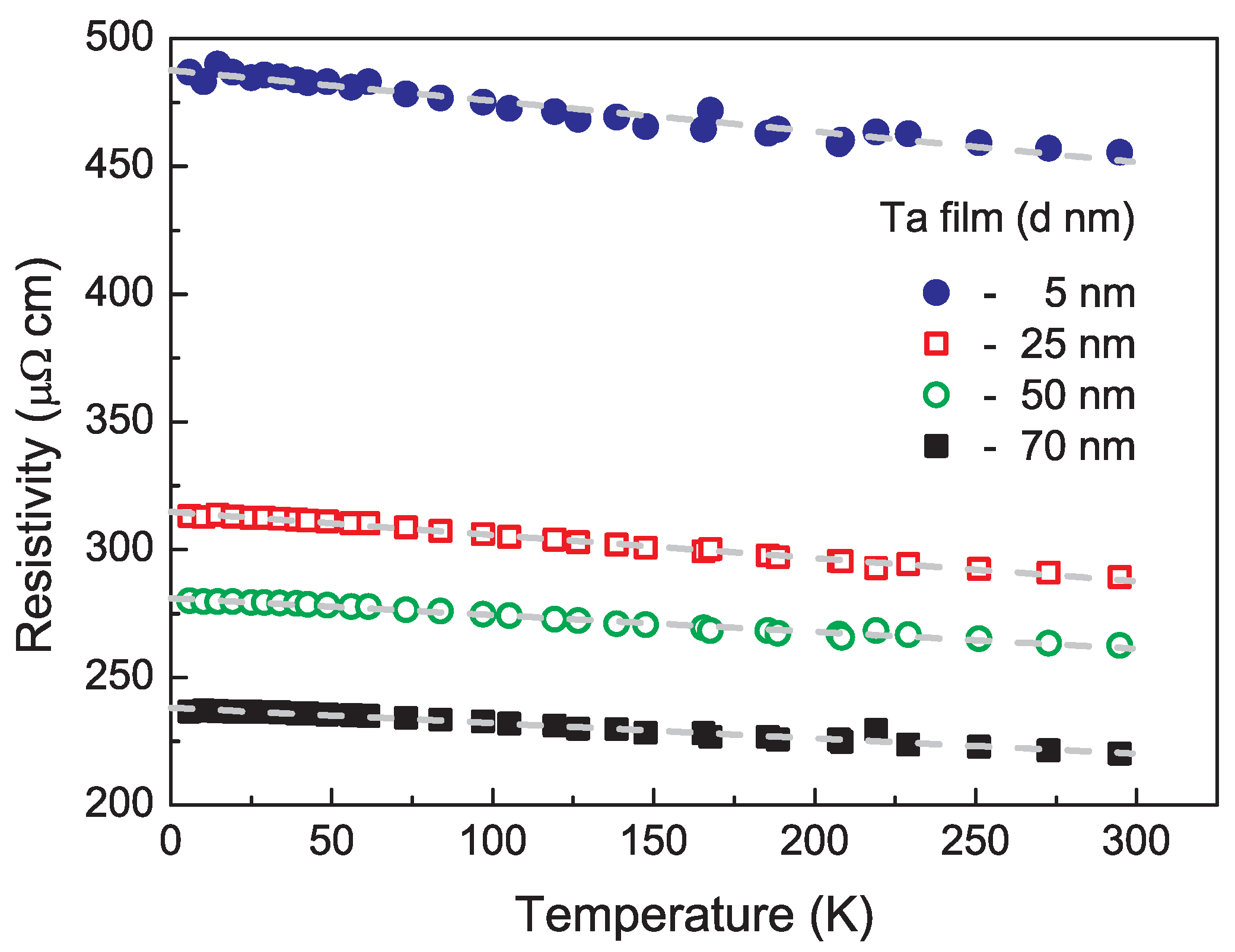
Sheet dc resistance of the rf sputtered Ta/Sitall films was measured in a wide temperature range on cooling from room temperature down to 5 K. For that, the film samples were mounted on a cold finger of the helium cryostat (RTI Cryomagnetic Systems, Moscow, Russia). The used multichannel electrical circuit allowed us to measure temperature dependence of sheet dc resistance simultaneously on several samples by four-point probe method.
Complex dielectric function spectra of the grown Ta/Sitall films were investigated in the wide photon energy range 0.8–8.5 eV with a J.A. Woollam VUV-Gen II spectroscopic ellipsometer (J.A. Woollam Co., Lincoln, NE, USA). The ellipsometry measurements were performed at two incident angles of 65
and 70
at room temperature. Additionally, the ellipsometry measurements were performed on the blank Sitall substrate. With only a single angle of incidence, the raw experimental data are represented by real values of the ellipsometric angles
and
. These values are defined through the complex Fresnel reflection coefficients for light-polarized parallel
and perpendicular
to the plane of incidence as follows
. The measured ellipsometric angles,
and
, were simulated using multilayer models available in the J.A. Woollam VASE software [
22].
4. Discussion
Using the obtained results, we discuss the dc electron transport properties of the studied
-Ta films of different thickness. A valuable information can be obtained from the Drude term parameters listed in
Table 1. It is generally known that mean path of conduction electrons
l is related to mean scattering time
as
, where
N is the concentration of free charge carriers, and
is the effective electron mass. Taking the Drude parameters
≃
10
s and
N ≃
10
cm
from
Table 1, we determine the average mean free path
l(70 nm) ≃ 3.12 Å for the Ta film of 70 nm thick. The estimated mean free path is smaller than the in-plane tetragonal (
)
-Ta lattice parameter a = 5.34 Å [
10]. It can be rather compared with the cubic (
)
-Ta lattice parameter 3.31–3.33 Å [
10]. The Drude parameters listed in
Table 1 suggest that the average mean free electron path slightly increases with increasing the Ta film thickness, thus
l(200 nm) ≃ 3.19 Å, and decreases with decreasing the Ta film thickness, for example,
l(25 nm) ≃ 3.06 Å. This means that the studied
-Ta films are strongly disordered, almost amorphous, where the high scattering probability restricts the average mean free electron path to
l ≃ 3.06–3.19 Å. At the same time, using the Drude parameters, one can estimate the dc conductivity,
. For example, this gives
(200 nm) ≃ 4100
cm
,
(70 nm) ≃ 3500
cm
, and
(25 nm) ≃ 3000
cm
. Their reciprocal values correspond to the optical resistivity data
given in
Table 1.
On the other hand, we found that the temperature variation of the dc transport,
, of the studied
-Ta films shows non-metallic behavior (
< 0) with negative TCR (
). The determined (
,
) values, as well as (
,
) values, well fit the range of the Mooij plot for highly disordered or amorphous metals having negative TCR and show the similar trend, implying that the physics of the studied Ta films is driven by static disorder [
1,
5]. Moreover, the acquired (
,
) dependence indicates on the general trend of a stronger degree of disorder in the thinner Ta films.
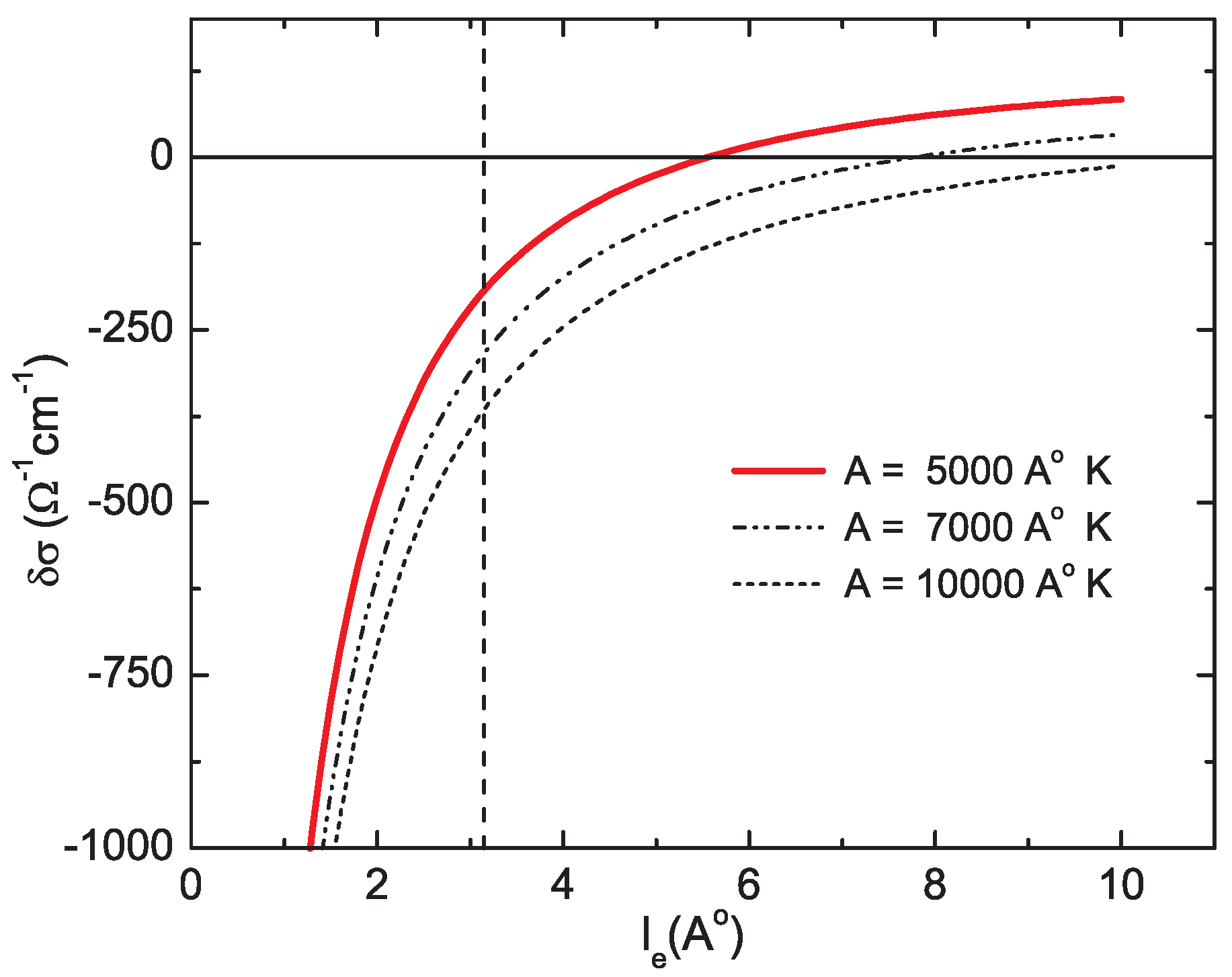
The correlation between TCR (
) and resistivity
, and, in particular, the phenomenon of negative TCR in disordered metals [
1], were considered and qualitatively evaluated by many researchers [
2,
3,
4,
5,
6,
7] in terms of weak localization effect [
8]. As a rule, the weak localization correction is small and in 3D metals is determined as follows
where
and
are an average mean free path of electrons between elastic and inelastic scattering, respectively, and
is the diffusion length [
5]. For an estimate at
T = 300 K one can admit that
,
P = 1. We take for
A = 5000 Å K from the results by Tsuei [
5]. Then,
≃ 17 Å, and for the mean free path
≃ 3–5 Å the diffusion length will be
≃ 4.1–5.3 Å. By using Equation (
3), we can estimate
in disordered metals, using
,
P = 1 [
5]. In
Figure 5 we plot
as a function of the mean elastic free electron path
for different values of the parameter
A = 5000, 7000, and 10,000 Å K. As one can see from the plot, for the average mean free electron path
l ≃ 3.06–3.19 Å, peculiar of the studied disordered
-Ta films, the effect of weak localization correction could achieve
~ – (180–360)
cm
. Thus, on one hand, the acquired in the present study (
,
) values, as well as (
,
) values, well fit the range of the Mooij plot for highly disordered or amorphous metals having negative TCR. On the other hand, we evaluated that the effect of weak localization correction could achieve here
~ – (180–360)
cm
only. However, this is far less than the estimated above dc conductivity variation in the studied Ta films of different thickness, namely,
(200 nm) ≃ 4100
cm
,
(70 nm) ≃ 3500
· cm
, and
(25 nm) ≃ 3000
· cm
. Therefore, there must be some additional reasons, which cause the observed pronounced dc conductivity changes.
One simple reason may be related to the effect of oxygen contamination and possible formation of chemically stable Ta oxides, such as TaO
and/or Ta
O
in the grown Ta films. However, the XRD analysis of the grown Ta films did not reveal any clear traces of Ta oxides in the grown Ta films. In addition, as we mentioned, we did not expect that concentration of oxygen defects, which can be caused by oxygen presence at a background level in using Ar gas, will be notably thickness dependent. Moreover, the bandgap value for sub-stoichiometric and stoichiometric TaO
and Ta
O
films is reported to be comprised in the spectral range 3.9–5.5 eV [
25,
26,
27]. In the present study, we observed a pronounced increase of the higher-energy Lorentz band around 5.5 eV, simultaneously with a sharp decrease of the Drude contribution only for the thinnest Ta film of about 5.0 nm thick (see
Figure 4e). In fact, from the present spectroscopic ellipsometry study, we conclude that the non-metallic character of the dielectric function response of the grown
-Ta films is associated with the presence of the intense Lorentz band peaking around 2 eV, which is strongly superimposed with the free charge carrier Drude response at low photon energies (see
Figure 3a–e and
Figure 4a–f). Moreover, we found that with increasing degree of disorder in the thinner Ta films, as indicated by increasing absolute value of their TCR, the intensity of the Lorentz band at 2 eV increases, whereas the intensity of the Lorentz band at 4 eV decreases (see
Table 1). The observed decrease of the Lorenz band at 4 eV in the thinner Ta films indicates that the effect of oxygen contamination is comparatively small and therefore cannot be responsible for the observed optical conductivity changes.
However, we noticed that our data provide apparent analogies to the dielectric function behavior reported for TaN
layers grown at different deposition temperatures (200–400
C) [
28]. By the way, here, the content of oxygen in the films was estimated at 3% only. The growth phase map [
21] suggests that, for the deposition conditions, the film composition is single-phase metastable
-TaN
for all deposition temperatures from 100 to 600
C (see Figure 7 of Ref. [
21]). The reported TaN
dielectric function range from metallic to non-metallic character, depending on the substrate temperature. The most pronounced metallic character exhibits the TaN
layer deposited with the highest substrate temperature of 400
C. In fact, this points on the defect annealing effect, indicating that the observed behavior of the dielectric function of the TaN
layers studied by Mistrik et al. [
28] is driven by static disorder. In addition, the optical properties of TaN were studied by spectroscopic ellipsometry and detailed DFT ab initio band structure calculations by Matenoglou et al. [
29]. It was shown that, along with the contribution from the Drude term describing the intraband absorption within the Ta 5d
band that intercepts the Fermi level, the additional Lorentz band was also observed at low photon energies around 1.9 eV.
Thus, we found that with increasing degree of disorder in the thinner Ta films, as indicated by increasing absolute value of their TCR, the Drude contribution due to intraband absorption within the Ta 5d
band at the Fermi level decreases due to localization effects. The associated optical spectral weight is recovered in the range of the higher-energy Lorentz bands at 2, 4, and 6–8 eV. Recently, we have shown that electron localization in the formed metallic magnetic clusters in the Kondo-lattice metal Tb
PdSi
leads to opening the pseudo-gap in the conduction band of itinerant electrons and appearance of the Mott-Hubbard-like interband optical transitions [
11,
12,
13,
14]. In the disordered Ta films, the observed low-energy transitions at around 2 and 4 eV may have some association with d
d
⇄ d
d
Mott-Hubbard-like electron correlations [
11,
12]. In this case, the observed decrease of the free charge carrier conductivity (Drude) with increasing the disorder degree, accompanied by the changes of intensities of the Mott-Hubbard-like bands, may indicate opening the pseudo-gap in the conduction band of itinerant electrons and global reconstruction of the band structure in disordered metals, associated with the many-body Anderson localization effects. This leads to the accelerated decrease of the Drude conductivity with increasing degree of disorder and can explain the observed pronounced dc conductivity variation in the studied Ta films. Though, this hypothesis requires further verification by theoretical band structure calculations for
Ta, as well as comprehensive experimental investigation of the temperature dependence of dielectric function spectra, by using, for example, spectroscopic ellipsometry approach.
Interestingly, for the ultrathin Ta film of about 5.0 nm thick, the Drude dc conductivity limit drops below the weak localization limit for disordered metals
≃ 3300
· cm
. Simultaneously, the global band structure reconstruction occurs (see
Figure 4e,f). Namely, the intensity of the optical band with the energy
~ 2 eV becomes essentially suppressed, instead, the higher-energy Lorentz band at
~ 5.5 eV becomes tremendously pronounced. One simple reason for this may be related to the effect of oxygen contamination and the formation of chemically stable Ta oxides, such as TaO
and/or Ta
O
, which, in principle, may be peculiar for the ultrathin Ta film, as we discussed earlier. However, another possible origin, associated with the nearly many-body localized state, cannot be excluded. According to the results of our atomic force microscopy study of the Sitall substrate, its profile shows the height variation of 1–3 nm, (which constitutes from 20% to 60% of the nominal film thickness) at the lateral scale 50–100 nm [
30]. We may propose that the roughness profile, with the peculiar long-range disorder, compared to the Ta lattice spacing, may enhance the Anderson localization, resulting in the formation of the nearly many-body localized electron state [
31]. In this case, the system may exhibit spectral gaps having different hierarcy of scales. The issue of the surface roughness on the possible formation of the many-body localized electron state requires more experimental and theoretical investigations.


