Article

Transparent Conducting Film Fabricated by Metal Mesh Method with Ag and Cu@Ag Mixture Nanoparticle Pastes

1
Department of Graphic Arts Information Engineering, Pukyong National University, Busan 48547, Korea
2
School of Material Science and Engineering, Ulsan National Institute of Science and Technology (UNIST), Ulsan 44919, Korea
*
Author to whom correspondence should be addressed.
Metals 2017, 7(5), 176; https://doi.org/10.3390/met7050176
Submission received: 7 March 2017 / Revised: 18 April 2017 / Accepted: 11 May 2017 / Published: 16 May 2017
(This article belongs to the Special Issue Metal Matrix Composites)

Abstract

:
Transparent conducting electrode film is highly desirable for application in touch screen panels (TSPs), flexible and wearable displays, sensors, and actuators. A sputtered film of indium tin oxide (ITO) shows high transmittance (90%) at low sheet resistance (50 Ω/cm2). However, ITO films lack mechanical flexibility, especially under bending stress, and have limitation in application to large-area TSPs (over 15 inches) due to the trade-off in high transmittance and low sheet resistance properties. One promising solution is to use metal mesh-type transparent conducting film, especially for touch panel application. In this work, we investigated such inter-related issues as UV imprinting process to make a trench layer pattern, the synthesis of core-shell-type Ag and Cu@Ag composite nanoparticles and their paste formulation, the filling of Ag and Cu@Ag mixture nanoparticle paste to the trench layer, and touch panel fabrication processes.

Graphical Abstract

1. Introduction

Transparent conducting electrode film is highly desirable for application in touch screen panels, flexible organic light emitting diode (OLED), and wearable displays, sensors, and actuators [1,2,3,4,5]. Metal nanoparticles have been used for conducting electrodes by using various fabrication process. One-step direct nanoimprinting of gold nanoparticles was reported by using hexanethiol self-assembled monolayer (SAM)-protected gold particles and polydimethylsiloxane (PDMS) mold [6]. Gold nanoparticles were also imprinted by PDMS mold on the polyimide film, and an organic field effect transistor device was fabricated [7]. The direct imprinting process using a PDMS mold leaves metal nanoparticles on top of the film substrate so that it has limited application in transparent touch screen panel (TSP) fabrication. Silver conductive ink was patterned on the PDMS stretchable substrate by stencil printing to make organic thin film transistor (OTFT) devices [8]. The OTFT device had excellent stretchability up to 150%, but the pattern width was 50 µm due to the stencil printing process, thus limiting the application in TSPs. The direct imprinting and screen printing processes have the merits of being simple processes operated at ambient condition. However, they result in an embossed pattern on the film substrate, so they may not withstand such hard mechanical stresses as bending and stretching.
In this work, we synthesized both Ag and cost-effective Cu@Ag nanoparticles for application to the large size touch screen panels. Indium tin oxide (ITO) has been widely used in transparent conducting electrodes (TCEs) to make small TSPs used in smartphones. However, ITO conductors cannot be used in large TSPs over 15 inches due to the trade-off between high transparency and low electrical resistance required for the operation of touch screen panels and the requirement of increasing the thickness of ITO thin films to lower the electrical resistance. Of the transparent conducting materials such as carbon nanotubes (CNTs), graphene, conducting polymer (PEDOT: PSS; poly (3,4-ethylenedioxythiophene) polystyrene sulfonate), and metal nanostructures, silver nanoparticles and silver-coated copper (Cu@Ag) nanoparticles have high potential for application in large TSPs, including flexible and stretchable versions. This is due to the suitability of the silver nanoparticle paste to the metal mesh-type transparent conducting electrode. In the metal mesh method, the transparent electrodes are patterned by using the trench filling process. In this method, a narrow engraved trench (~2.5 µm) pattern is formed by coating a ultra violet (UV) curing resin on the substrate film and then pressing with a transparent mold followed by UV exposure and demolding. The gap between the trenches is over 100 µm, so the visible light transmittance of the metal mesh film is over 88% while the resistivity of the Ag nanoparticle paste is less than 10 Ω·cm by the percolation mechanism. Metal mesh TCEs also have the merit of easy hard coating layer formation on top of a trench pattern layer filled with silver particles compared to the imprinting or screen printing processes with embossed silver electrode patterns.

2. Materials and Methods

2.1. Ag and Cu@Ag Composite Nanoparticles and Paste

The synthetic process of silver (Ag) nanoparticles is shown in Figure 1. First, butylamine (160 g) (Sigma-Aldrich, Seoul, Korea) and ethanol (320 g) (Sigma-Aldrich, Seoul, Korea) were mixed at 23–25 °C; then, oleic acid (surfactant, 213 g) (Sigma-Aldrich, Seoul, Korea) was added and the mixture solution was heated to 70 °C. After cooling to 55 °C, silver acetate (106.8 g) (Sigma-Aldrich, Seoul, Korea) was added and the temperature was maintained at 40 °C, while aqueous hydrazine (Sigma-Aldrich, Seoul, Korea) and polyvinylpyrrolidone (Sigma-Aldrich, Seoul, Korea) mixture solution was added at a rate of 4 mL/10 min for 10 min. After 30 min stabilization, the silver nanoparticles were precipitated and separated by repeated washing with ethanol.
The Cu@Ag composite nanoparticles were made by electroplating silver onto copper (Cu) nanoparticles [9]. The process is as follows. First, Cu nanoparticles made by a similar method mentioned above for the Ag nanoparticles were washed with HCl aqueous solution and with deionized water. The washed Cu nanoparticles were dispersed in deionized water with polyacrylate surfactant. To this solution were added the AgNO3 and NH4OH mixture aqueous solution and reacted with stirring followed by separation and drying. The resulting Cu@Ag nanoparticles were recovered by centrifuge and washed with water to remove the capping agent. The Ag and Ag@Cu nanoparticles were mixed with bisphenil—an epoxy acrylate resin dissolved in the diethylene glycol monoethyl ether acetate (ECA) (Sigma-Aldrich, Seoul, Korea) solvent with dispersant BYK-9076 obtained from BYK Additives & Instruments, Wesel, Germany [10]. The resulting Ag/Cu@Ag nanoparticle paste was further mixed by using a three roll-mill (Exakt, Oklahoma City, OK, USA) followed by degassing and rolling.

2.2. Metal Mesh Mold and Trench Layer Patterning

The embossed metal mesh mold was fabricated by using photolithographic and electroplating method. The engraved trench layer pattern was made by first coating a photosensitive UV resin on the optical grade polyethylene terephthalate (PET) and then pressing with the embossed metal mold (less than 10 psi) followed by UV exposure (150 mJ) and demolding. The trench screen panel and engraved pattern of trench layers consisting of sensor and bezel electrodes are shown in Figure 2. As shown in Figure 2, the width of the narrow sensor electrodes was 1–2.5 μm, and the width of the bezel electrodes was 20–50 μm. After filling the Ag/Cu@Ag paste into the trench layers of the sensor and bezel electrodes, the remaining Ag/Cu@Ag pastes on top of the PET film substrate needed to be wiped out. However, during this process, the Ag/Cu@Ag paste in the engraved area of the trench layer is also removed by the wiping process. In order to prevent the wiping-out of filled Ag/Cu@Ag nanoparticle paste from the engraved trench layers, the embossed metal mesh mold was designed to have many small embossed patterns, especially inside the wide bezel electrode area. This design of embossed metal mesh mold was found to be very effective in reducing the wiping-out of the Ag/Cu@Ag paste filled into the engraved trench layer.

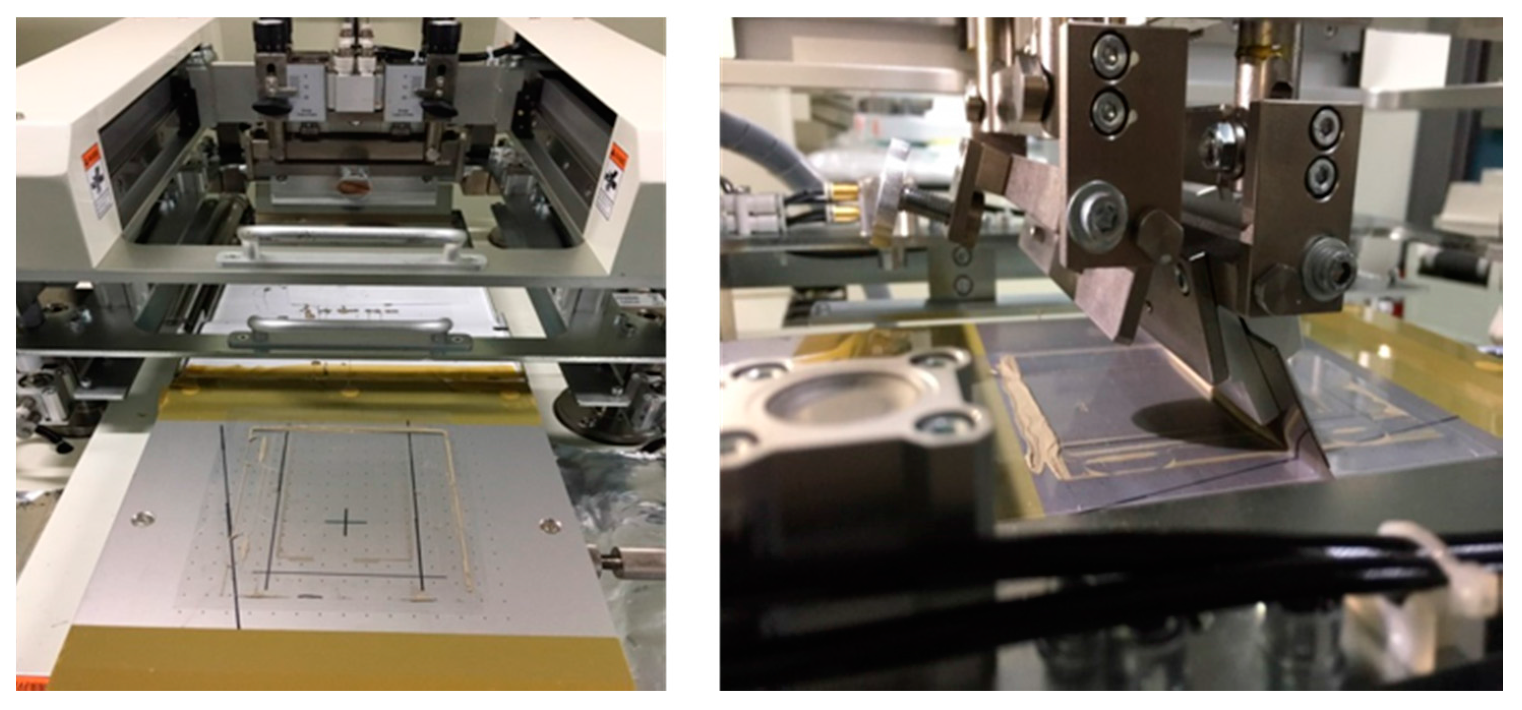
2.3. Filling of Ag/Cu@Ag Nanoparticle Paste and Wiping of Residual Paste

The Ag/Cu@Ag nanoparticle paste was filled into the engraved trench layers consisting of sensor and bezel electrodes on the PET substrate film by using a doctoring machine made by Mino Co. [11] (Gifu, Japan), as shown in Figure 3. The formulations of the photosensitive UV resins are shown in Table 1. Of these UV resins, sample UVT-5-1 was found to give adequate flexibility and demolding property from the metal mold after UV exposure. After filling Ag/Cu@Ag nanoparticle paste into the engraved trench layer, the residual paste was wiped off the embossed part of PET film substrate by a wiping cloth, followed by post-heating of the filled silver paste.

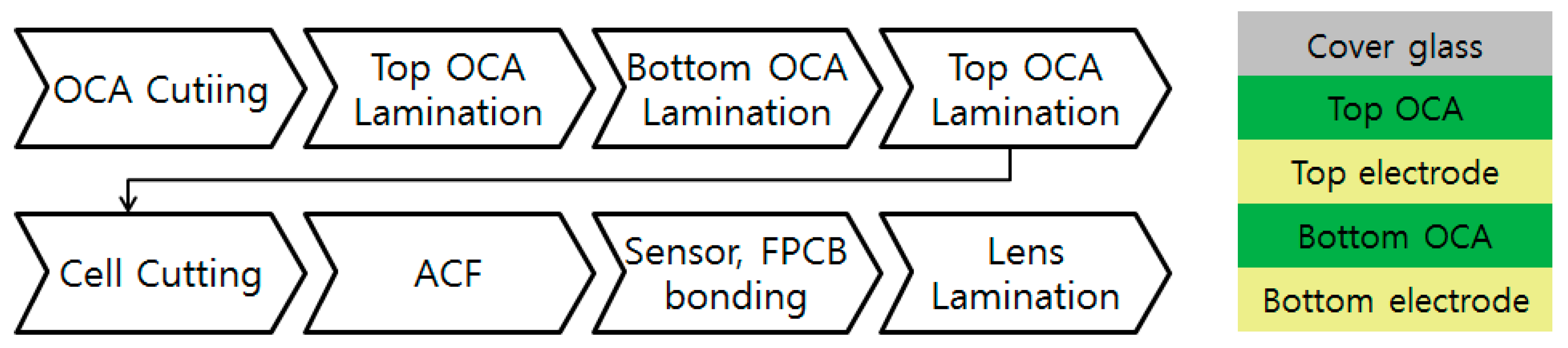
2.4. Fabrication of Touch Panel by Using Metal Mesh Films

The structure and fabrication process of the touch panel are shown in Figure 4, utilizing the two transparent metal mesh films made with Ag/Cu@Ag nanoparticle pastes. After lamination of the cover glass and the top/bottom part of the touch sensor with optically clear adhesive (OCA) films, the touch panel circuits and controller were bonded to the flexible printed circuit board (f-PCB) using anisotropic conductive film (ACF).

3. Results

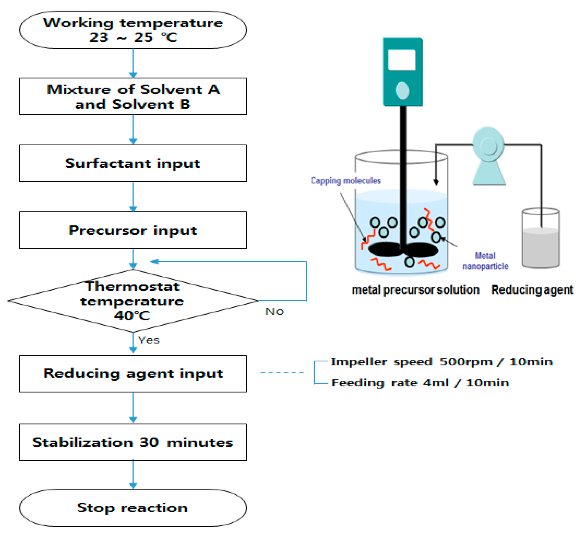
3.1. Ag Nanoparticle Synthesis and Paste Properties

Scanning electron microscope (SEM) images of the synthesized Ag nanoparticles are shown in Figure 5. Ag powder in paste (1) exhibited nanoparticles in the 1–25 nm range, which can promote sintering at lower temperature. Ag powder in paste (2) exhibited the aggregation of Ag nanoparticles, and the Ag powder in paste (3) contained large Ag nanoparticles. The three Ag pastes were formulated with different Ag nanoparticles, and their conductivities were checked after coating and thermal curing on PET substrate films. Table 2 indicates that the Ag paste in paste (1) cured at 180 °C for 20 min showed high conductivity. This may be due to the partial sintering of Ag nanoparticles in Ag paste (1) and concurrent high packing density of Ag nanoparticles, thus promoting effective percolation.

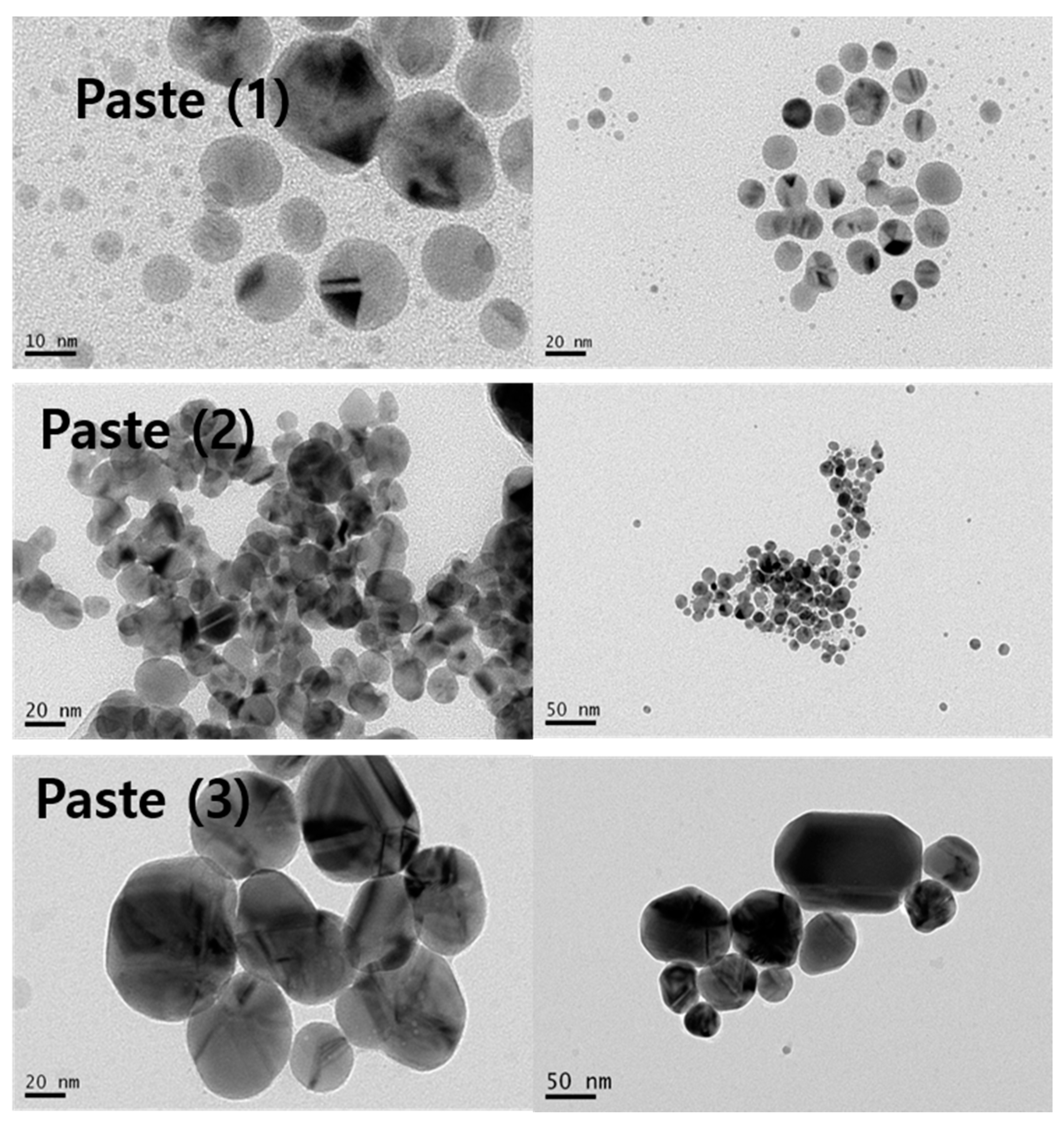
3.2. Cu@Ag Composite Nanoparticles and Paste Properties

The Cu@Ag composite nanoparticles were synthesized by electroplating method, as described in the experimental part with Ag contents of 20, 30, 40 wt %. The Cu@Ag nanoparticle pastes were formulated with binder polymer content of 4 and 2 wt %, as shown in Table 3. The viscosity of the Cu@Ag nanoparticle paste with 2 wt % of binder polymers was higher than that of 4 wt % paste, while the sheet resistance was lower in the case of metal paste with 2 wt % of binder polymers. However, the conductivity of the Cu@Ag nanoparticle paste was lower than that of the pure Ag nanoparticle paste in Table 2. Therefore, a new metal paste was made by mixing pure Ag and Cu@Ag nanoparticle with 30 wt % Ag in the ratio of 8:2, 5:5, and 2:8 by weight. As shown in Table 4, the Ag/Cu@Ag mixture paste (3) showed low surface resistance for touch panel application along with good filling property into trench layer pattern.

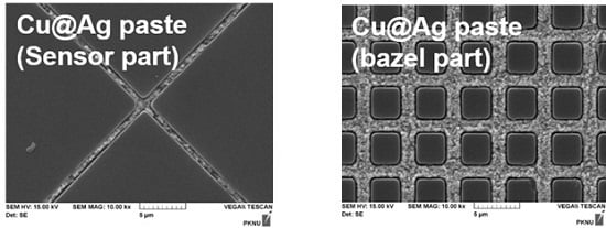
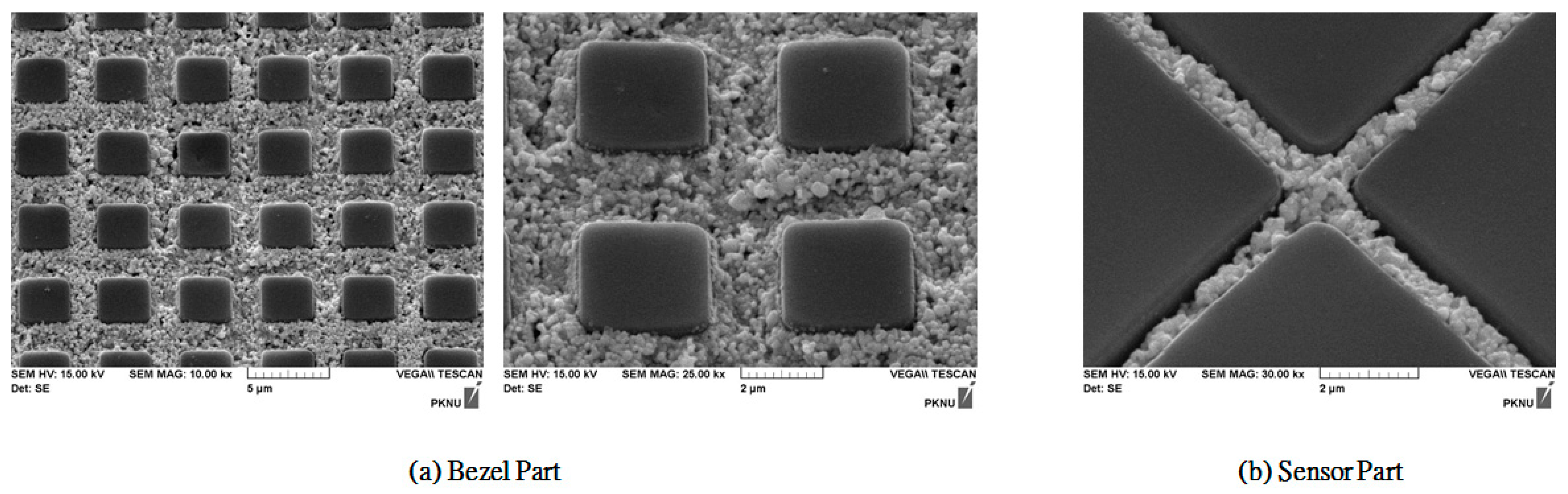
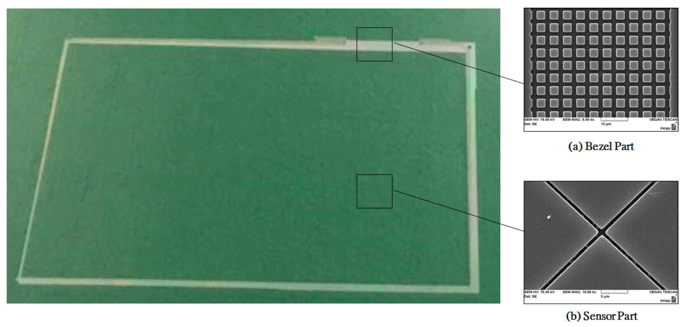
3.3. Inlay Filling of Ag and Cu@Ag Mixture Paste and Performance of Touch Screen Panel

The Ag and Cu@Ag mixture paste was filled into the pattered trench layer by using a doctoring machine made by Mino Co., Gifu, Japan. Figure 6 shows that the mixture paste could be filled 80–90% by first filling and almost 100% by second filling with the doctoring machine. After optimizing the metal paste by mixing Ag and Cu@Ag paste at 20:80 wt % ratio and filling process of the mixture paste into the trench layer, the touch panel module was fabricated and the properties were as follows. The optical property of the metal mesh transparent film was L*: 0.95 and b*: 0.53, suitable for touch screen panel application. The uniformity of the width of the trench layer with 1 µm design was found to be 0.93 ± 0.007, and the sheet resistance of the metal mesh with 1 µm width were 14.57 ± 0.487 Ω/cm2), with uniformity of 3.26%. The capacitance change before (Cm = 6.68 pF) and after (Cm = 4.85 pF) 10,000 bending cycles at 60 rpm and radius R = 10 mm also met the specification value of 28.37%, which was within the acceptance range of 30%.

4. Conclusions

In this work, we investigated such inter-related issues as the synthesis of core-shell-type Ag and Cu@Ag composite nanoparticles and their paste formulation UV imprinting process to make a trench layer pattern, filling of Ag and Cu@Ag mixture nanoparticle paste to the trench layer, and touch panel fabrication processes. After optimizing the metal paste by mixing Ag and Cu@Ag paste at 20:80 wt % ratio and filling process of the mixture paste into the trench layer, a touch panel module was fabricated and the properties were as follows. The optical property of the metal mesh transparent film was L*: 0.95 and b*: 0.53. The uniformity of the width of the trench layer with 1 µm design was found to be 0.93 ± 0.007, and the sheet resistance of the metal mesh with 1 µm width were 14.57 ± 0.487 Ω/cm2 with uniformity of 3.26%, suitable for touch screen panel application.

Acknowledgments

This work was supported by a Research Grant of Pukyong National University (2016 year).

Author Contributions

Su Yong Nam and Lee Soon Park conceived and designed the experiments; Hyun Min Nam, Duck Min Seo, Hyung Duk Yun and Gurunathan Thangavel performed the experiments.

Conflicts of Interest

The authors declare no conflict of interest.

References

  1. Park, S.I.; Xiong, Y.; Kim, R.H.; Elvikis, P.; Meitl, M.; Kim, D.H.; Wu, J.; Yoon, J.; Yu, C.J.; Liu, Z.; et al. Printed assemblies of inorganic light-emitting diodes for deformable and semitransparent displays. Science 2009, 325, 977–981. [Google Scholar] [CrossRef] [PubMed]
  2. Yu, Z.; Niu, X.; Liu, Z.; Pei, Q. Intrinsically Stretchable Polymer Light-Emitting Devices Using Carbon Nanotube-Polymer Composite Electrodes. Adv. Mater. 2011, 23, 3989–3994. [Google Scholar] [CrossRef] [PubMed]
  3. Sekitani, T.; Nakajima, H.; Maeda, H.; Fukushima, T.; Aida, T.; Hata, K.; Someya, T. Stretchable active-matrix organic light-emitting diode display using printable elastic conductors. Nat. Mater. 2009, 8, 494–499. [Google Scholar] [CrossRef] [PubMed]
  4. Han, T.H.; Jeong, S.H.; Lee, Y.; Seo, H.K.; Kwon, S.J.; Park, M.H.; Lee, T.W. Flexible transparent electrodes for organic light emitting diodes. J. Inf. Disp. 2015, 16, 71–84. [Google Scholar] [CrossRef]
  5. Choi, Y.M.; Kim, K.W.; Lee, E.; Jo, J.; Lee, T.M. Fabrication of a single layer metal-mesh touchscreen sensor using reverse-offset printing. J. Inf. Disp. 2015, 16, 37–41. [Google Scholar] [CrossRef]
  6. Ko, S.H.; Park, I.; Pan, H.; Grigoropoulos, C.P.; Pisano, A.P.; Luscombe, C.K.; Fréchet, J.M. Direct nanoimprinting of metal nanoparticles for nanoscale electronics fabrication. Nano Lett. 2007, 7, 1869–1877. [Google Scholar] [CrossRef] [PubMed]
  7. Park, I.; Ko, S.H.; Pan, H.; Grigoropoulos, C.P.; Pisano, A.P.; Fréchet, J.M.; Lee, E.S.; Jeong, J.H. Nanoscale patterning and electronics on flexible substrate by direct nanoimprinting of metallic nanoparticles. Adv. Mater. 2008, 20, 489–496. [Google Scholar] [CrossRef]
  8. Suh, Y.D.; Jung, J.; Lee, H.; Yeo, J.; Hong, S.; Lee, P.; Lee, D.; Ko, S.H. Nanowire reinforced nanoparticle nanocomposite for highly flexible transparent electrodes: borrowing ideas from macrocomposites in steel-wire reinforced concrete. J. Mater. Chem. C 2017, 5, 791–798. [Google Scholar] [CrossRef]
  9. Park, M.; Im, J.; Shin, M.; Min, Y.; Park, J.; Cho, H.; Park, S.; Shim, M.B.; Jeon, S.; Chung, D.Y.; et al. Highly stretchable electric circuits from a composite material of silver nanoparticles and elastomeric fibers. Nat. Nanotechnol. 2012, 7, 803–809. [Google Scholar] [CrossRef] [PubMed]
  10. BYK Additives & Instruments. Available online: http://BYK.com/kr (accessed on 7 March 2017).
  11. Mino International Ltd. Available online: http://mino.co.jp (accessed on 7 March 2017).
Figure 1. Synthesis of metal nanoparticles.
Metals 07 00176 g001
Figure 2. Touch sensor panel and scanning electron microscope (SEM) images of engraved (a) bezel electrodes and (b) sensor electrode patterns made by UV imprinting process with embossed metal mold.
Metals 07 00176 g002
Figure 3. Filling process of Ag/Cu@Ag nanoparticle paste with doctoring machine.
Metals 07 00176 g003
Figure 4. Structure and fabrication process of touch screen panel. ACF: anisotropic conductive film; OCA: optically clear adhesive.
Metals 07 00176 g004
Figure 5. Field emission scanning electron microscopy (FE-SEM) images of synthesized Ag nanoparticles in Ag pastes (1) to (3).
Metals 07 00176 g005
Figure 6. SEM images of filled Ag/Cu@Ag mixture paste in (a) bezel and (b) sensor parts of metal meshes touch screen panel.
Metals 07 00176 g006
Table 1. Formulation of photosensitive UV resin for imprinting process to make trench layers.
SampleUV OligomerUV MonomerPhotoinitiator
F-130 (g)EEEA (g)HDDA (g)PI-TPO 25 wt % in EEEA (g)
UVT-1-17.01.01.80.2
UVT-2-16.02.01.80.2
UVT-3-15.03.01.80.2
UVT-3-25.03.01.80.4
UVT-4-14.04.01.80.2
UVT-4-24.04.01.80.4
UVT-5-13.05.01.80.2
UVT-5-23.05.01.80.4
F-130 ; Ebecryl 8411 (Allnex, Sydney, Australia), EEEA ; Etoxyetoxy ethyl acrylate(Sigma-Aldrich, Seoul, Korea), HDDA ; Hexane diol diacrylate (Sigma-Aldrich, Seoul, Korea), PI-TPO (Ciba, Basel, Switzerland).
Table 2. Synthetic condition of Ag nanoparticles and the formulation of Ag nanoparticle pastes. ECA: Diethylene glycol monoethyl ether acetate.
Ag PasteAg Powder Synthetic ConditionAg PowderBinder PolymerSolventAdditive
88 wt %4 wt %7 wt %1 wt %
Ag Paste (1)Acid value: 100 / Injection rate: 10 mL/min (40 min)Ag powder (1)Bisphenol-A Epoxy acrylateECABYK-754
Ag Paste (2)Acid value: 100 / Injection rate: 40 mL/min (10 min)Ag powder (2)Bisphenol-A Epoxy acrylateECABYK-754
Ag Paste (3)Acid value: 50 / Injection rate: 40 mL/min (10 min)Ag powder (3)Bisphenol-A Epoxy acrylateECABYK-754
Ag PasteThermal curing condition and conductivity
100 °C, 20 min130 °C, 20 min180 °C, 20 min
Ag Paste (1)-13–18 mΩ3–4 mΩ
Ag Paste (2)-11–13 mΩ4–6 mΩ
Ag Paste (3)-8–10 mΩ4–5 mΩ
Table 3. Formulation of Cu@Ag nanoparticle pastes and properties.
Cu@Ag PastesCu@Ag PowderCu@Ag Paste Formulation (wt %)
Cu@Ag PowderBinder PolymerSolventAdditiveSheet Resistance (4 Point, Ω/cm2)
Bisphenol-A Epoxy AcrylateECABYK-9076
Cu@Ag paste (1)Cu@Ag (Ag: 20 wt %)88471500–600
Cu@Ag paste (2)Cu@Ag (Ag: 30 wt %)88471380–480
Cu@Ag paste (3)Cu@Ag (Ag: 40 wt %)88471200–300
Cu@Ag paste (4)Cu@Ag (Ag: 20 wt %)88291450–500
Cu@Ag paste (5)Cu@Ag (Ag: 30 wt %)88291250–300
Cu@Ag paste (6)Cu@Ag (Ag: 40 wt %)88291150–200
Table 4. Formulation of Ag and Cu@Ag nanoparticle mixture paste and properties.
Cu@Ag PastesAg and Cu@Ag Paste Mixture Formulation (wt %)
Cu@Ag PowderAg PowderBinder PolymerSolventAdditiveSheet Resistance (4 Point, Ω/cm2)
Bisphenol Epoxy AcrylateECABYK-9706
Paste (1)Cu@Ag 70.4 wt %Ag 17.6 wt %29155–80
Paste (2)Cu@Ag 44.0 wt %Ag 44.0 wt %29130–45
Paste (3)Cu@Ag 17.6 wt %Ag 70.4 wt %29113–15

