1. Introduction
Titanium and titanium alloys are widely used in lightweight constructions in the aerospace industry due to their good corrosion stability and high specific strength. In aircraft structures mainly Ti6Al4V is used due to the well balanced properties, however the amount of titanium β-alloys (e.g., Ti
15V
3Cr
3Sn
3Al) is continuously rising especially in areas where high strength and excellent corrosion resistance is required [
1]. The new light-weight concepts in the latest generation of aircraft have highlighted the use of titanium alloys as joining parts to light-weight materials such as aluminum and fiber reinforced plastics (CFRP) in order to avoid galvanic corrosion. To overcome the failure modes like rivet rash on titanium rivet heads or loss of paint adhesion on titanium crack stopper the adhesive bonding can be applied. However long-term stable adhesion on titanium is still an issue and the key to success is to realize a suitable surface treatment [
4]. Currently wet-chemical bath processes partially based on toxic and environmentally-hazardous compounds are used as pretreatment for titanium. Plasma enhanced chemical vapor deposition (PECVD) of silicone dioxide films at atmospheric pressure seems to be an alternative to these wet-chemical methods.
This work focuses on a linearly extended and scalable DC arc plasma source (LARGE) for the deposition of silica layers on titanium alloys. The influence of different working distances (2 cm, 4 cm) is evaluated for hexamethyldisiloxane (HMDSO) as a precursor. The surface characterization of resulting films was done by X-ray photoelectron spectroscopy (XPS), Fourier transform infrared (FTIR) spectroscopy and scanning electron microscopy (SEM). Adhesive bonding tests were performed and the results were compared to the wet chemical anodising treatment “NaTESi”, which was used as standard pretreatment process. The influence of the different plasma treatment parameters on adhesion properties was evaluated using the wedge test.
2. Experimental Section
2.1. Material
For this study the titanium alloys Ti
6Al
4V and Ti
15V
3Cr
3Sn
3Al are used. In Ti
6Al
4V alloy, the main alloying elements are α-stabilizer aluminum and β-stabilizer vanadium. This alloy belongs to α + β titanium alloys. The Ti
15V
3Cr
3Sn
3Al alloy belongs to β titanium alloys due to the main β-stabilizer elements vanadium and chromium, tin is considered a neutral element since it has no influence on the α/β phase boundary [
1].
Polished samples (Ra = 60 nm, measured with AFM) are used with the dimension of 25 × 25 mm2 and a thickness of 2 mm for XPS and FTIR investigations. The sample dimensions for the mechanical tests are 150 × 150 × 2 mm3.
2.2. Surface Preparation
All titanium samples are processed with the same conditioning steps prior to the plasma process: cleaning with the alkaline cleaner using P3 Almeco 18 (Henkel AG and co. KGaA, Düsseldorf, Germany) at 65 ± 3 °C for 15 min, alkaline etching with Turco 5578 (Henkel AG and co. KGaA, Düsseldorf, Germany) at 95 ± 3 °C for 5 min using a concentration of 500 g/L [
2].
2.3. Plasma Treatment
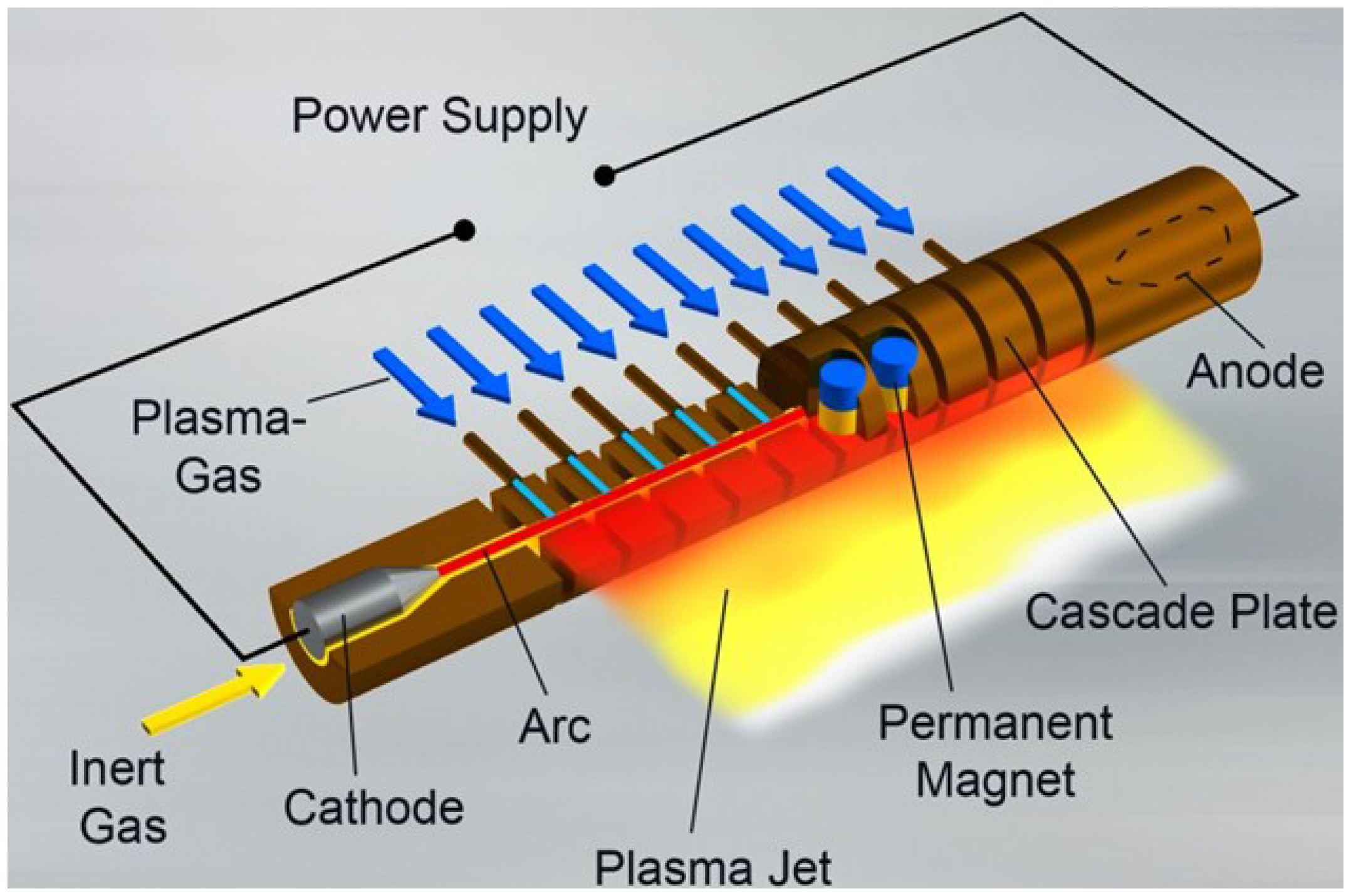
The LARGE plasma source is used for the deposition of SiO
2 films. Using this plasma generator a linearly extended and stabilized DC arc plasma at atmospheric pressure is generated. The principle of the plasma source is described in
Figure 1. The arc occurs between opposite electrodes. The distance of the electrodes is essential for the working width of the plasma source and is variable using a cascade construction. A 150 mm long arc is used for the experiments presented in this paper. A gas mixture (compressed air, nitrogen or argon plus molecular gas) evenly circulates around the arc perpendicular to the arc axis. The plasma gas flows through the plasma source at high speed and drives the excited chemical species out of the source. The precursor is injected outside of the plasma source using a remote gas feeding system and will be activated by a diffusion process with the plasma jet. The remote gas feeding system for SiO
2 deposition film is made from anodized AlMgSi1. A detailed description of the plasma source and the remote gas feeding system is given in [
3].
Figure 1.
Principle of the long arc generator (LARGE) plasma source (linearly extended DC arc).
The thin SiO
2 films on titanium alloys presented in this article are deposited using a 150-mm-LARGE plasma source and hexamethyldisiloxane (HMDSO) as precursor. The sample was moved in front of the plasma source at distances varying from 20 mm up to 60 mm. The precursor was heated up to 130 °C and injected into the plasma jet using a remote gas feeding system.
Table 1 summarizes the main process parameters for the deposition of SiO
2 films.
Table 1.
Process parameter for SiO2 deposition with the LARGE plasma source at atmospheric pressure.
| Process parameters | Value |
|---|
| Plasma gas | 70 Std. L/min Ar + 50 Std. L/min N2 |
| Remote gases | 30 Std. L/min N2 + 30 Std. L/min O2 |
| Precursor | 30 g/h HMDSO |
| Working distance | 2 to 6 cm |
| Working width | 150 mm |
| Current | 75 A |
| Substrate velocity | 10 m/min |
2.4. Surface Characterization
The deposited SiO2 films are analyzed by means of Fourier transform infrared (FTIR) spectroscopy (Bruker, Ettlingen, Germany), X-ray photoelectron spectroscopy (XPS) (Physical Electronics, Eden Prairie, MN, USA) and scanning electron microscope (SEM) (Jeol, Tokyo, Japan). Polished samples are necessary for the film characterization methods (Ra = 60 nm).
The chemical composition of the films is analyzed by FTIR reflection spectroscopy using IRspecXL®Fraunhofer IWS (Bruker, Ettlingen, Germany). The FTIR spectra are obtained by applying p-polarized light with an incidence angle of 73° and a spectral range between 6000 m−1 and 400 cm−1, resolution 2 cm−1 and 32 scans.
The XPS investigations are performed using a Quantum 2000 spectrometer (Physical Electronics, Eden Prairie, MN, USA) equipped with an Al Kα (1486.6 eV) monochromatic source, operating at 15 kV. The diameter of the spot is set at 200 µm with a take-off angle of 45° and pass energy of 117.4 eV. High-resolution spectra are charge-compensated by setting a binding energy of the C1s peak to 284.8 eV. Peaks are fitted (Gaussian/Lorentzian curves) after background subtraction (Shirley type) using the multipack 8.2 software (Physical Electronics, Eden Prairie, MN, USA). The depth profile of the samples is measured applying Ar+ bombardment with an acceleration voltage of 2 keV and a sputtering rate of 7 nm/m (calibrated on SiO2).
A Jeol JSM-6320F field emission scanning electron microscope (Jeol, Tokyo, Japan) is used for high resolution optical surface and interface analysis. The lateral resolution is app. 1.5 nm. Pt is sputtered onto the samples to reduce charging. Samples are fractured in liquid nitrogen (cryo fracture) to allow a side view in the fractured oxide and coupling films.
2.5. Test Method
The bonding strength and aging behavior of titanium joints is evaluated by using the wedge test. The test is conducted according to the German standard DIN 65448. Two pretreated sheets 150 × 150 × 2 mm3 are bonded together with epoxy-based film adhesive FM 73 M and cured in an autoclave at a temperature of 120 °C and a pressure of 0.25 MPa. Five samples with the width of 25 mm are cut out. The aging test is carried out in a conditioning chamber at 95% RH and 50 °C. The crack growth is microscopically monitored after 1.25 h, 24 h, 48 h, 96 h, 168 h, 336 h and 500 h. After the aging period the samples are separated to investigate the failure loci.
3. Results and discussion
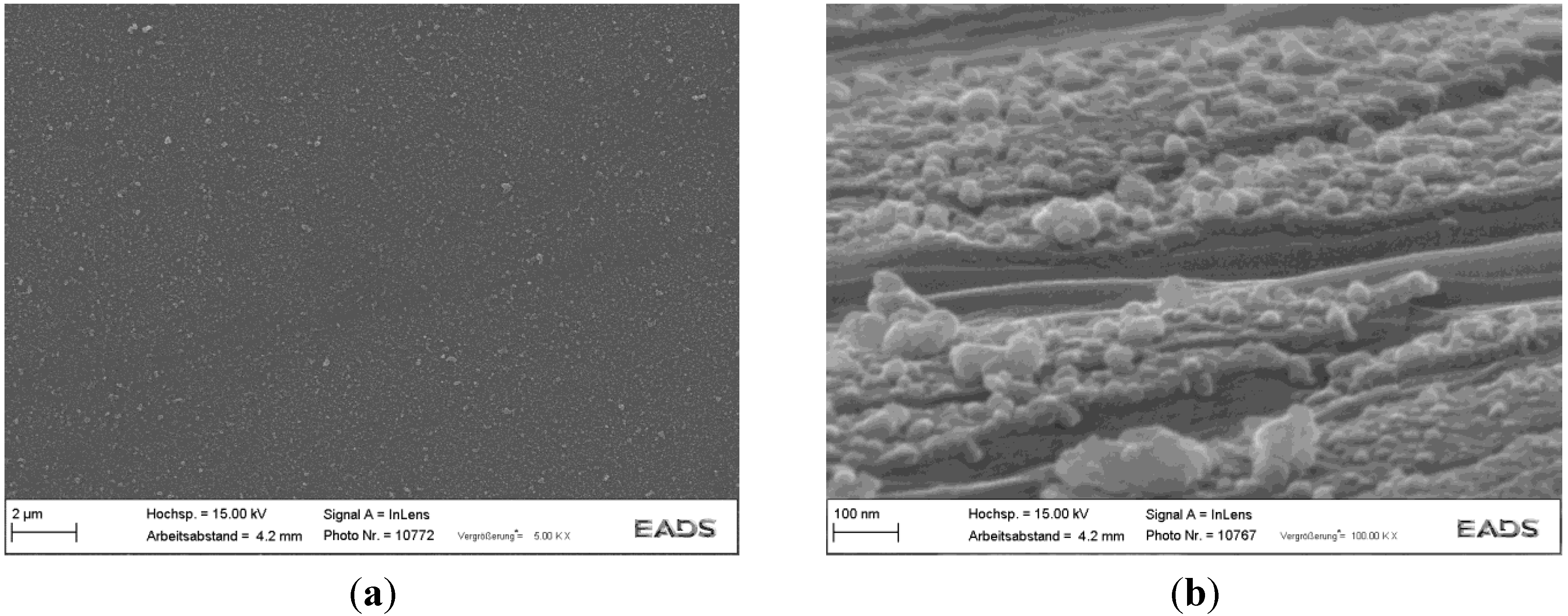
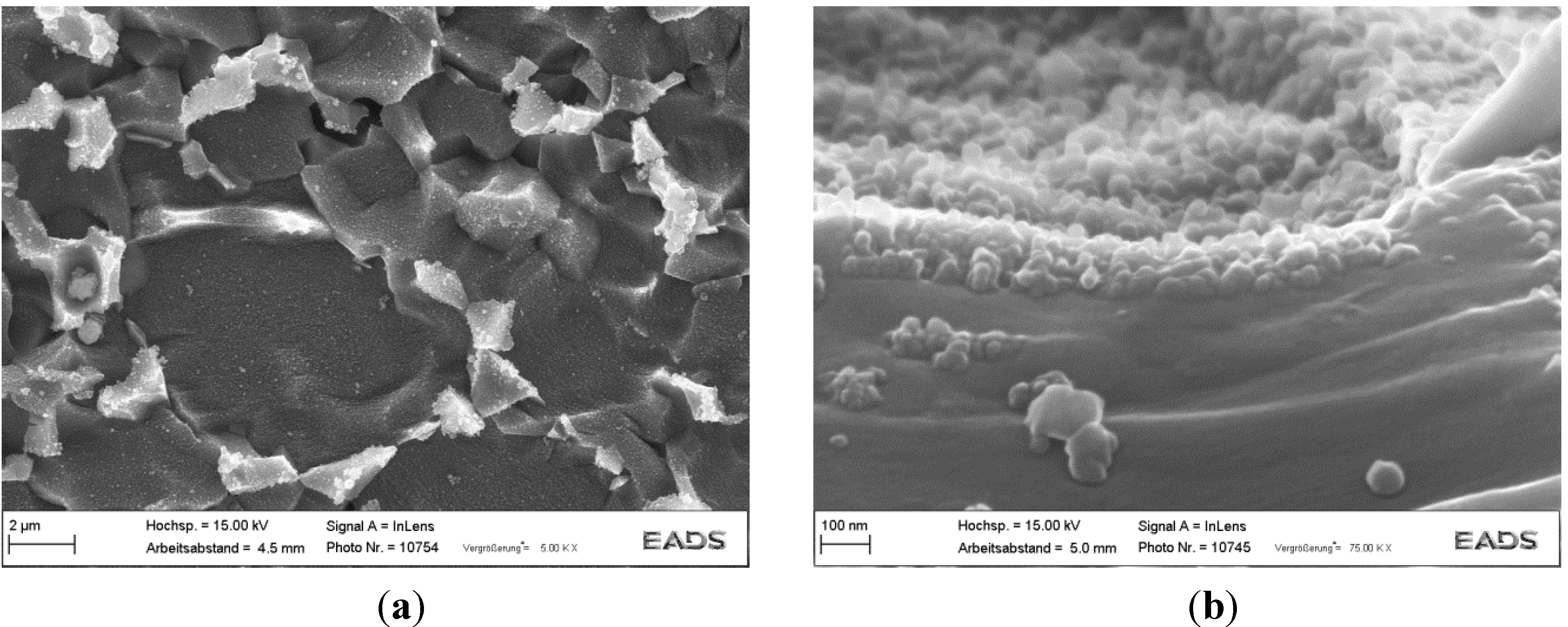
Figure 2 and
Figure 3 exhibit a different morphology after atmospheric plasma based deposition at 2 cm working distance and 50 nm nominal layer thickness on Ti
6Al
4V respectively Ti
15V
3Cr
3Sn
3Al. The titanium samples are wet-chemical treated using Turco 5578 before plasma treatment. Ti
6Al
4V sample shows the typical macro roughness after alkaline etching (
Figure 2a). The surface of both titanium samples is completely covered by the HMDSO derived film and exhibits a globular structure (
Figure 2a and
Figure 3a). The SEM micrograph of the cryo fractures can be used to determine the thickness of the deposited oxide layers. In both cases the thickness of the deposited plasma film is between 30 nm and 46 nm.
Figure 2.
SEM micrographs after film deposition on Ti6Al4V (a) top view; (b) Cryo fracture of Ti6Al4V.
Figure 3.
SEM micrographs after film deposition on Ti15V3Cr3Sn3Al (a) top view; (b) Cryo fracture of Ti15V3Cr3Sn3Al.
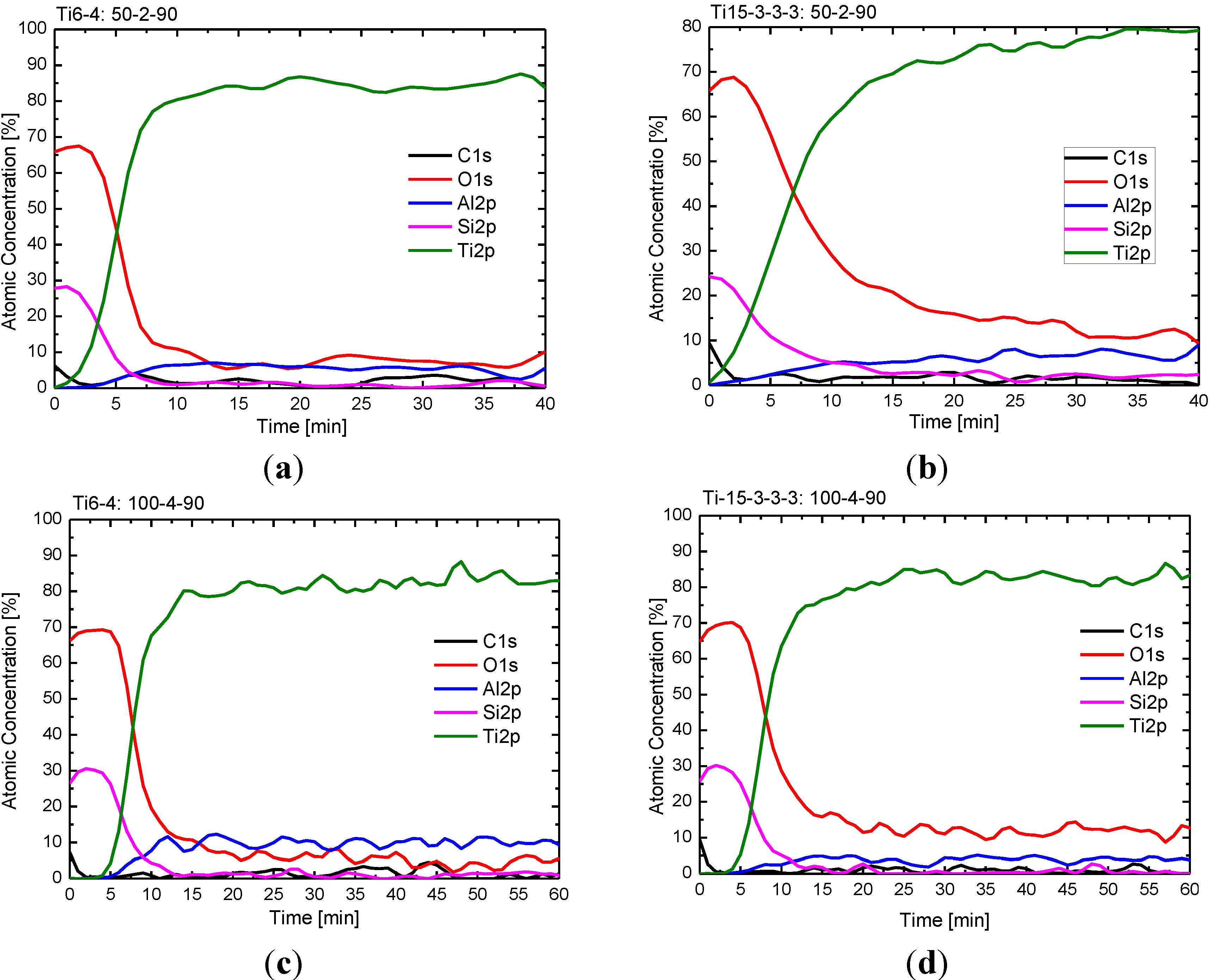
The XPS depth profile (
Figure 4) shows very similar film composition for both titanium alloys and different treatment parameters (50 nm nominal oxide thickness/2 cm working distance; 100 nm nominal oxide thickness/4 cm working distance).
The stoichiometric composition (
Table 2) of the deposited plasma oxide layer shows the O/Si ratio of 2.5/1 for Ti
15V
3Cr
3Sn
3Al and 2.6/1 for Ti
6Al
4V. The difference to the literature value of 2/1 for SiO
2 can be attributed to the oxygen content which can be assigned to surface contamination or functional groups (C–O, O–C=O, C=O). The carbon content on the surface of about 7% can be partly assigned to the surface contamination. The depth profile shows that after first few minutes the carbon content is reduced to 3–5 at%. This value is caused by plasma fragmentation/polymerization of the HMDSO precursor [
2].
Figure 4.
Depth profile of the hexamethyldisiloxane (HMDSO) derived coating obtained with the supply rate of 7 nm/min (sample nomenclature: Ti15-3-3-3 = Ti15V3Cr3Sn3Al, Ti6-4 = Ti6Al4V, 50 (nominal thickness [nm])–2 (working distance [cm])–90 (tilting angle/sample position)). (a) Ti6-4: 50-2-90; (b) Ti15-3-3-3: 50-2-90; (c) Ti6-4: 100-4-90; (d) Ti15-3-3-3: 100-4-90.
Table 2.
Chemical composition of the titanium surface after atmospheric plasma deposition (sample nomenclature: Ti15-3-3-3 = Ti15V3Cr3Sn3Al, Ti6-4 = Ti6Al4V, 50 (nominal thickness [nm])–2 (working distance [cm])–90 (tilting angle/sample position)).
| Elements | C [at%] | O [at%] | Si [at%] |
|---|
| Ti15-3-3-3: 50-2-90 | 7.0 | 66.7 | 26.3 |
| Ti15-3-3-3: 100-4-90 | 6.2 | 67.3 | 26.5 |
| Ti6-4: 50-2-90 | 5.4 | 68.2 | 26.4 |
| Ti6-4: 100-4-90 | 7.7 | 66.5 | 25.8 |
| Chemical compound | Contamination/SiOxCy | Contamination/SiOx | SiOx |
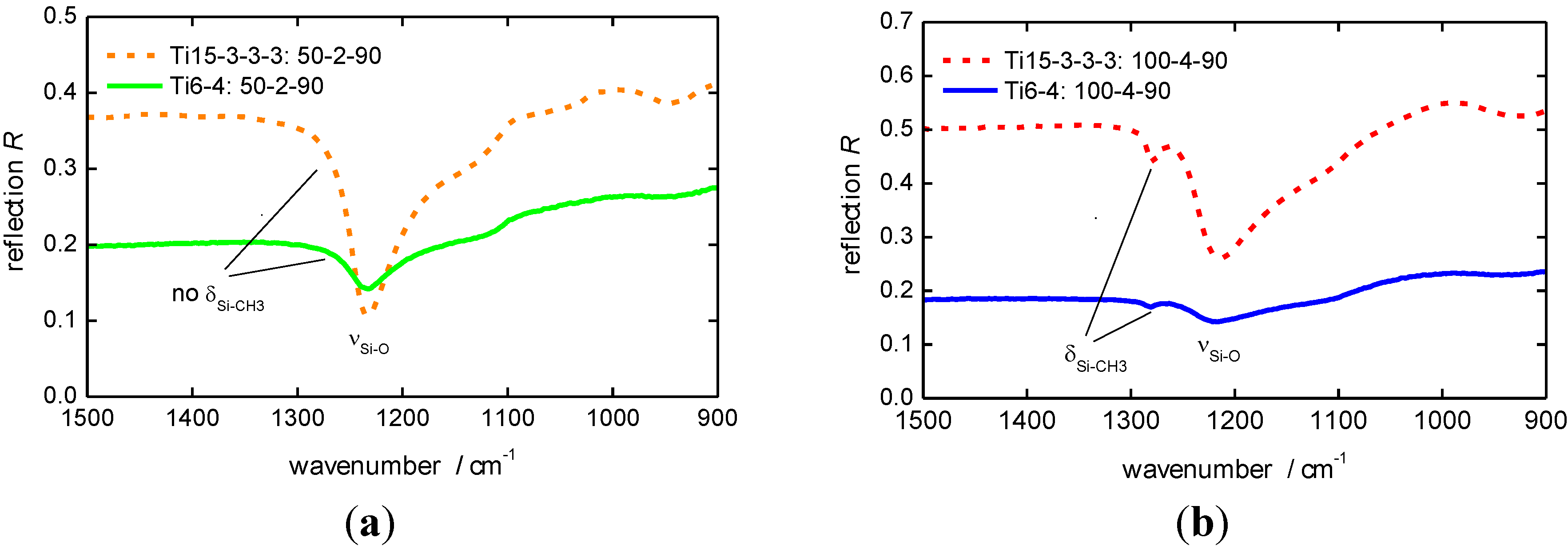
The availability of the Si-CH
3 group is necessary to achieve a good adhesion of titanium alloys [
2].
Figure 5 shows that the surface, treated at 2 cm working distance and 50 nm nominal oxide thickness, exhibits no Si–CH
3 groups for both titanium alloys. In 4 cm working distance the Si–CH
3 groups are generated (
Figure 5b). The FTIR results are comparable to the wedge test results of bonded titanium samples due to the availability of Si–CH
3 groups on the surface (
Figure 6). The best adhesion results could be achieved with SiO
2 films containing Si–CH
3 groups.
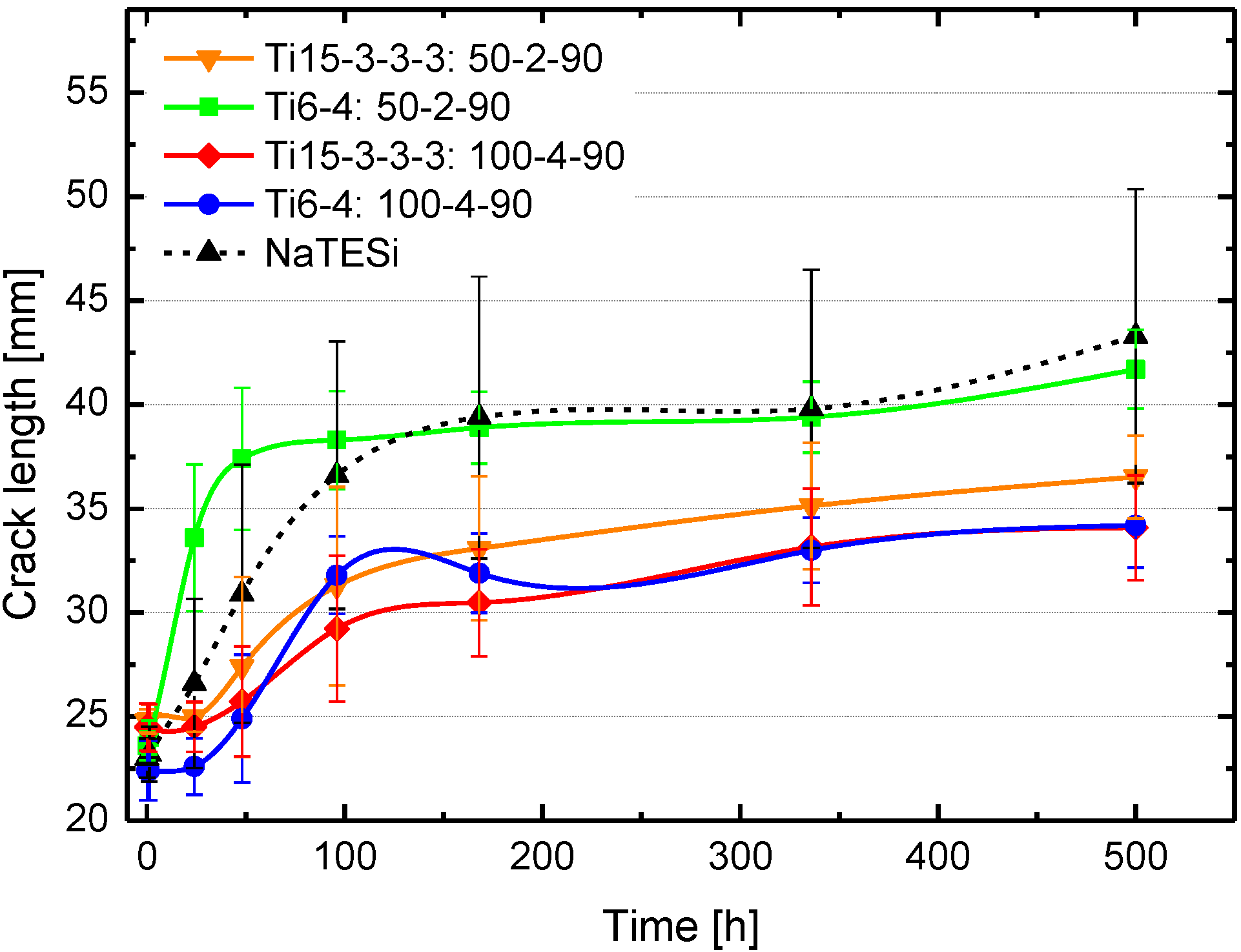
The wedge test is performed to evaluate the long-term stability of bonded titanium alloys after the plasma treatment. All parameters lead to a comparable initial crack length and bonding strength, respectively. The initial crack length is between 23 mm and 25 mm for all parameters. All samples feature a lower total crack length using the atmospheric plasma deposition compared to the NaTESi anodizing process after 500 h exposure to hot/wet conditions. The titanium samples treated at 4 cm working distance and 100 nm nominal layer thickness feature a crack length of 34.2 ± 2.5 mm, while the samples treated at 2 cm working distance and 50 nm nominal oxide thickness show a lower crack length 41.7 ± 1.9 mm for Ti
6Al
4V and 36.5 ± 1.9 for Ti
15V3Cr
3Sn
3Al. The crack length correlates with the working distance and film thickness. With increasing working distance and film thickness the crack length decreases. Those wedge test results correlate to the FTIR results shown below. Samples which exhibit the Si-CH
3 group on the surface show a lower crack length compared to the samples without the Si-CH
3 groups. The adhesion force of the titanium alloy bonding depends on the morphology of the surface and the chemistry of the adhesion layer [
4]. Due to the very different morphology of the investigated alloys, it is assumed that the chemical bonding process is the crucial part for the adhesion process.
Figure 5.
FTIR spectra of deposited film on titanium alloy (a) 50 nm nominal oxide layer thickness and at 2 cm working distance; (b) 100 nm nominal oxide layer and at 4 cm working distance.
Figure 6.
Crack propagation of pre-treated titanium samples (sample nomenclature: Ti-15-3-3-3 = Ti15V3Cr3Sn3Al, Ti-6-4-Ti = 6Al4V, 50 (nominal thickness [nm])–2 (working distance [cm])–90 (tilting angle/sample position)).


