Article

Sb2S3/Sb2O3 Heterojunction for Improving Photoelectrochemical Properties of Sb2S3 Thin Films

1
Key Laboratory for Nonferrous Vacuum Metallurgy of Yunnan Province, Kunming University of Science and Technology, Kunming 650093, China
2
Faculty of Metallurgical and Energy Engineering, Kunming University of Science and Technology, Kunming 650093, China
3
State Key Laboratory of Complex Non-Ferrous Metal Resources Clean Utilization, Kunming University of Science and Technology, Kunming 650093, China
*
Author to whom correspondence should be addressed.
Metals 2025, 15(5), 478; https://doi.org/10.3390/met15050478
Submission received: 17 March 2025 / Revised: 21 April 2025 / Accepted: 22 April 2025 / Published: 24 April 2025

Abstract

We prepared antimony metal films via electrodeposition, followed by the synthesis of Sb2S3 films through a chemical vapor phase reaction. Finally, an Sb2O3 film was deposited onto the Sb2S3 film using a chemical bath method, successfully constructing a heterojunction photocathode of Sb2S3/Sb2O3; the synthesized Sb2S3/Sb2O3 heterojunction is classified as a Type I heterostructure. The resulting Sb2S3/Sb2O3 heterojunction exhibited a photocurrent density of −0.056 mA cm−2 at −0.15 V (vs. RHE), which is 1.40 times higher than that of Sb2S3 alone under simulated solar illumination. Additionally, the Sb2S3/Sb2O3 heterojunction demonstrated a lower carrier recombination rate and a faster charge transfer rate compared to Sb2S3, as evidenced by photoluminescence and electrochemical impedance spectroscopy tests. For these reasons, the Sb2S3/Sb2O3 heterojunction obtained a hydrogen precipitation rate of 0.163mL cm−2 h−1, which is twice the hydrogen precipitation rate of Sb2S3, under the condition of 60 min of light exposure. The significant enhancement in photoelectrochemical performance is attributed to the formation of the Sb2S3/Sb2O3 heterojunction, which improves both carrier separation and charge transfer efficiency. This heterojunction strategy holds promising potential for visible light-driven photoelectrochemical water splitting.

1. Introduction

Today, global population growth, rising energy consumption, and climate change pose significant threats to future energy security. Conventional fossil fuel combustion is a major source of greenhouse gas emissions, and over time, these resources are increasingly unable to meet humanity’s growing energy demands. As a result, the search for cost-effective, sustainable, renewable, and clean alternative energy sources has become a key area of research. This effort aims not only to meet daily energy needs but also to address the environmental challenges associated with traditional energy production [1,2,3,4]. Since Fujishima and Honda first demonstrated the photoelectrochemical decomposition of water for hydrogen production using TiO2 photoanodes in 1972, photoelectrochemical (PEC) water splitting has made significant progress. Solar-driven PEC water splitting has become one of the most promising methods for hydrogen production. The construction of efficient and stable photoelectrodes is the critical factor in the PEC water decomposition system [5,6].
In recent years, antimony–sulfur compounds (such as Sb2S3, Sb2Se3, etc.) have gained significant attention from researchers due to their suitable bandgap and high light absorption properties. Among these, antimony sulfide (Sb2S3), which is highly abundant and environmentally friendly, stands out for its high light absorption coefficient. Its narrow bandgap, which aligns well with the solar spectrum, makes it an excellent candidate for photoelectrodes. As a result, Sb2S3 has attracted considerable interest in the study of photoelectrochemical water splitting [7]. Sb2S3 is a direct bandgap p-type semiconductor with excellent properties, including a narrow bandgap (~1.72 eV) which matches well with the solar spectrum, and band edges Ec = 0.22 V (vs. NHE) and Ev = 1.94 V (vs. NHE) [8] that align well with the solar spectrum. It also boasts a high light absorption coefficient (α ~ 105 cm−1), low cost, a low melting point (~550 °C), and outstanding stability in air and humidity [9,10,11]. These exceptional characteristics make Sb2S3 a highly attractive material for photovoltaic applications. Therefore, it is widely used in photodetectors [12,13,14], supercapacitors [15,16], solar cells [17,18,19], and photocatalysts [20,21]. However, the PEC performance of pristine Sb2S3 remains significantly lower than its theoretical potential [22]. The photogenerated carriers in Sb2S3 under light illumination exhibit limited diffusion lengths and short lifetimes. They are also less stable due to significant electron–hole recombination rates and insufficient charge mobility [23]. This is because the Fermi energy levels of the Sb2S3 photoelectrodes are pinned by deep energy level defects, leading to low separation and transport efficiency of the photogenerated carriers. To overcome these limitations, researchers have explored and investigated various modification techniques, including the construction of heterostructures, elemental doping, and the incorporation of co-catalysts.
Sb2O3 is an n-type semiconductor with a bandgap width of 3.0 eV, Ec = 0.32 V (vs. NHE), and Ev = 3.32 V (vs. NHE) [8,24]. Tigau [25] prepared Sb2O3 thin films using the evaporation method and found that the resulting polycrystalline thin films exhibited good crystalline quality, a face-centered cubic structure, and a lattice constant of a = 11.14 Å. The films also featured a selectively grown (222) crystal plane and demonstrated superior electronic conductivity at room temperature. Meanwhile, Sb2O3 also has strong UV absorption [26], optical refractive index [27], and electrochemical catalytic effect [28].
Research has been conducted on Sb2S3/Sb2O3 composite materials. Li et al. [29] modified TiO2 photoanodes using Sb2S3/Sb2O3, resulting in the creation of Sb2S3/Sb2O3/TiO2 composite photoanodes. Subsequent studies assessed the cathodic protection effectiveness of these composite photoanodes on 304 stainless steel, revealing improved performance relative to pure TiO2. The Sb2S3/Sb2O3/TiO2 composite photoelectrode demonstrated optimal performance to achieve an open circuit potential (OCP) of −0.76 V, which is significantly lower than the corrosion potential of 304 stainless steel. Additionally, Jiang et al. [30] successfully synthesized Sb2O3/Sb2S3 nanocomposite materials with n–n heterojunctions, utilizing them as photoanodes for photoelectrochemical water splitting, achieving a photocurrent density 40 times greater than that of bare Sb2O3 photoanodes. However, all previously reported Sb2S3/Sb2O3 composite materials have been employed exclusively as photoanodes. This study explores the potential of Sb2S3 as the photoactive layer at the bottom of photoelectrochemical cathodes, since its band gap is well positioned in relation to the energy distribution of the solar spectrum and it exhibits a high absorption coefficient in the visible light range. In contrast, Sb2O3 exhibits superior catalytic performance, strong corrosion resistance, and notable ultraviolet absorption properties, making it an ideal candidate for the catalytic layer at the top of the photoelectrochemical cathode. Through photoelectrochemical testing, we analyze and compare the photoelectrochemical properties of Sb2S3/Sb2O3 with those of Sb2S3, investigating photocurrent density, photogenerated charge carrier recombination rates, and charge transfer pathways.

2. Materials and Methods

2.1. Materials

Potassium antimony tartrate (K(SbO)C4H4O6 1/2H2O, AR, 500 g, 99.0%, Tianjin Windship Chemical Reagent Technology Co., Tianjin, China), ammonium chloride (NH4Cl, AR, 500 g, 99.5%, Tianjin Windship Chemical Reagent Technology Co., Tianjin, China), antimony trichloride (SbCl3, AR, 500 g, 99.0%, Aladdin, Shanghai, China), triethanolamine (TEA, AR, 500 mL, 98.0%, Hengxing Reagent, Tianjin, China), sulfur powder (S, AR, 500 g, 98.0%, Tianjin Windship Chemical Reagent Technology Co., Tianjin, China), ethanol (C2H5OH, AR, 2500 mL, 99.7%, Chengdu Cologne Chemical Co., Chengdu, China), sulfuric acid (H2SO4, AR, 2500 mL, 95.0~98.0%, Chuandong Chemical, Chongqing, China), hydrochloric acid (HCl, AR, 2500 mL, 98.0%, Chuandong Chemical, Chengdu, China), sodium hydroxide (NaOH, AR, 500 g, 96.0%, Tianjin Windship Chemical Reagent Technology Co., Tianjin, China), and fluorine doped tin oxide (FTO, Gu Luo glass, Luoyang, China) glass substrates (14–16 Ω cm−1, 25 mm × 15 mm, 2.2 mm) were acquired. All chemical products were of analytical grade and used as received without further purification.

2.2. Preparation of the Sb2S3/Sb2O3 Heterojunction

Preparation of Sb2S3 film—The synthesis of Sb2S3 was accomplished through the electrodeposition of antimony metal onto fluorinated tin oxide (FTO)-coated substrates, followed by annealing in a sulfur atmosphere. The electrolyte solution used was a mixed solution of potassium antimony tartrate (K2(Sb2(C4H2O6)2) at 5.5 mmol L−1 and ammonium chloride (NH4Cl) at 100 mmol L−1. The pH of the mixed solution was adjusted to 1.3 using 0.1 mol L−1 HCl, resulting in the final electrolyte solution, with a deposition potential of −0.8 V (vs. SCE) for a duration of 30 min. Subsequently, the deposited antimony metal was annealed in a sulfur-rich environment at 250 °C. The desired temperature was achieved by ramping at approximately 5 °C per min. In this process, the Sb metal was situated in zone 1 (250 °C), while elemental sulfur powder (1 g) was placed in zone 2 (200 °C). The vulcanization duration was 30 min, after which the assembly was allowed to cool to room temperature within the furnace [31,32].
Preparation of Sb2S3/Sb2O3 photoelectrode—Sb2O3 was prepared using a chemical bath deposition method. Specifically, 1.5 mL of triethanolamine was added to 60 mL of an SbCl3 solution, which was adjusted to a concentration of 0.05 M. Under continuous stirring, saturated NaOH was added to adjust the pH to 7.80. Following this preparation, the previously synthesized Sb2S3 was vertically immersed in the resulting solution and maintained at a temperature of 60 °C for 15 min to facilitate the formation of the Sb2S3/Sb2O3 heterojunction [30,33].

2.3. Characterization

The crystallization phase of all the samples was investigated using an X-ray diffractometer (Shimadzu, XRD-6000, Cu Kα radiation, λ = 0.154056 nm, Kyoto, Japen) in the diffraction angle region of 10–80°. Scanning electron microscopy (SEM, ZEISS Sigma 300, Carl Zeiss AG, Oberkochen, Germany) and a corresponding Energy Dispersive Spectrometer (EDS) were used to perform a fine analysis of the microstructure, micromorphology, and composition of the sample. The transmittance spectra of the samples were obtained using an UV–Vis–NIR spectrophotometer (PE lambda 750, PerkinElmer, Inc., Waltham, MA, USA) in a wavelength range of 200–1000 nm at room temperature. The elemental composition and chemical valence of the samples were studied by X-ray photoelectron spectroscopy (XPS, Thermo Scientific K-Alpha, Thermo Fisher Scientific, Waltham, MA, USA). Steady-state photoluminescence (PL) spectra were examined by an Edinburgh FLS1000(Edinburgh Instruments Ltd., Edinburgh, UK) spectrofluorimeter. Sb2S3 and the Sb2S3/Sb2O3 heterojunction were excited with an excitation light of 320 nm, and the emission spectra were tested from 230 to 850 nm.

2.4. PEC Measurements

All PEC measurements were performed in a three-electrode system, in which the sample, Pt electrode, and saturated calomel electrode (SCE) were used as working, counter, and reference electrodes, respectively. A 0.5 M H2SO4 solution was employed as the electrolyte. Light illumination was performed from the front of the electrode. A 300 W xenon lamp with an AM1.5G filter was used to simulate the global standard sunlight spectrum (AM1.5G 100 mW·cm−2, Xenon lamp and AM1.5G filter are from Beijing CEC Jinyuan, Beijing, China, the xenon lamp model is CEL-HXF300), and the scan rate of the linear sweep voltammetry was 2 mV/s. The test temperature was 25 °C, the pressure was atmospheric, and the diameter of the prepared photoelectrode was inserted into the solution to start the test. All work potentials were determined vs. RHE using the following Equation (1) [34]:
E v s . R H E = E v s . S C E + 0.2483 + 0.0591 × p H

3. Results and Discussion

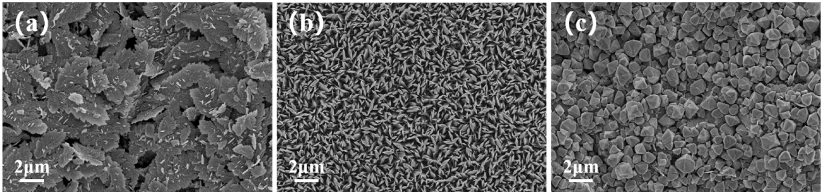
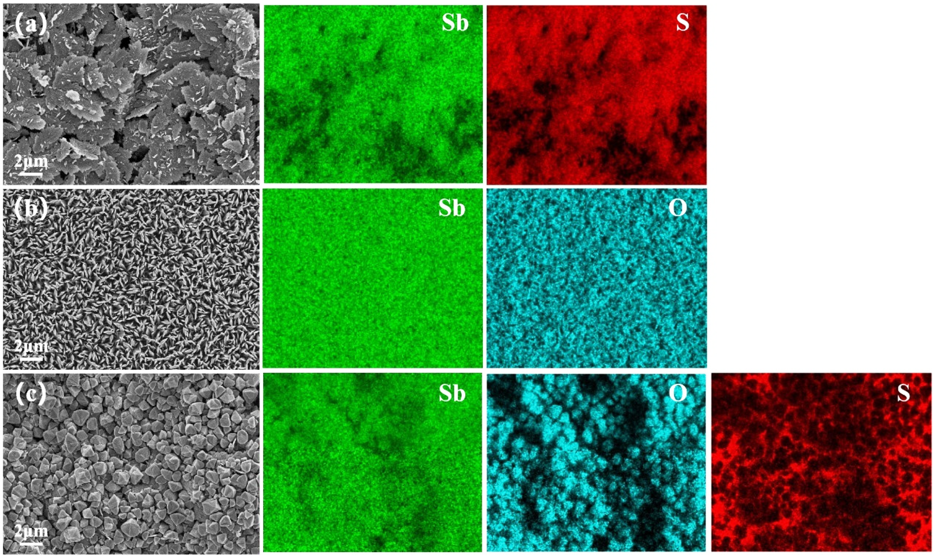
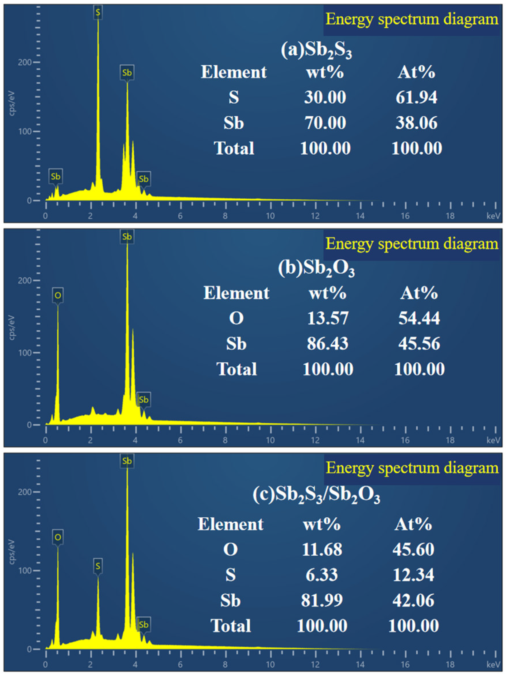
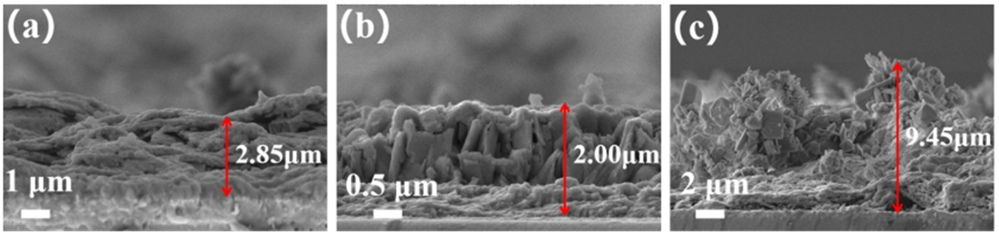
3.1. Characterization of the Phase Structure of Sb2S3 and the Sb2S3/Sb2O3 Heterojunction

The crystalline phase structures of monomeric Sb2S3 films and the Sb2S3/Sb2O3 heterojunction were analyzed and compared using X-ray diffraction (XRD) patterns. Figure 1 illustrates that the characteristic peaks of Sb2S3 thin films are located at 17.66°, 25.02°, 29.36°, and 32.48°, corresponding to the (120), (310), (211), and (212) crystallographic planes, respectively. These observations align with the orthorhombic phase of Sb2S3 (JCPDS 42-1393), wherein the (211) crystallographic plane is identified as the optimal growth orientation.
For the Sb2S3/Sb2O3 heterojunction samples, in addition to the peaks characteristic of Sb2S3, additional peaks at 13.80°, 27.76°, 32.16°, and 46.08° were detected. These peaks correspond to Sb2O3 (JCPDS 71-0365) and are associated with the (111), (222), (400), and (440) crystallographic planes, respectively, with the (222) plane being the preferred growth orientation. Furthermore, the peaks at 26.58°, 33.77°, 37.77°, 51.75°, 61.75°, and 65.74° are attributed to SnO2 from the FTO glass substrate. Notably, no additional impurity diffraction peaks were observed in the XRD spectra, indicating that samples with well-defined crystallinity were successfully obtained. The (120) and (310) crystal faces indeed exhibit higher diffraction intensity compared to the (211) crystal face. However, when processing the data using Jade, it was found that the proportion of the diffraction peaks corresponding to the (120) and (310) crystal faces is not very significant, while the (211) crystal face has a larger proportion in the diffraction peak at 29.36°. Therefore, the (211) crystal face is considered to be the optimal growth plane.
The surface morphologies of monolithic Sb2S3, Sb2O3, and the Sb2S3/Sb2O3 heterojunction were analyzed and compared using field emission scanning electron microscopy (SEM). As illustrated in Figure 2, the Sb2S3 films exhibited a bottom-up stacking of lamellar morphology, which facilitates greater absorption of visible light due to their increased exposed surface area. However, a significant number of pinholes were observed between the lamellae, which could allow direct contact of the electrolyte with the FTO glass substrate. This situation may compromise the photoelectrochemical performance and stability of Sb2S3.
In contrast, the Sb2O3 films comprised prismatic morphology with uniformly distributed smaller particles on the FTO glass substrate, indicating that the Sb2O3 films synthesized via chemical bath deposition possess good crystallization. The surface morphology of the Sb2S3/Sb2O3 heterojunction featured larger granular morphology attributed to Sb2O3. Notably, when Sb2O3 was grown on the Sb2S3 substrate, the morphology changed, and the growth of Sb2O3 effectively covered the existing pinholes in Sb2S3. This alteration addresses the issue of electrochemical performance degradation linked to those pinholes.
Additionally, the elemental distributions of monomeric Sb2S3, Sb2O3, and the Sb2S3/Sb2O3 heterojunction were investigated through energy dispersive X-ray spectroscopy (EDS) and mapping diagrams. As illustrated in Figure 3, the distribution of sulfur (S) and antimony (Sb) atoms within the selected range indicates a non-homogeneous distribution of S atoms in Sb2S3, which confirms the presence of multiple pinholes (Figure 3a). In contrast, the distribution of oxygen (O) and Sb atoms in the Sb2O3 film is notably uniform (Figure 3b). Furthermore, the mapping of O atoms in the Sb2S3/Sb2O3 heterojunction demonstrates that the observed large granular morphology corresponds to Sb2O3 (Figure 3c).
Figure 4 shows the EDS spectrum and compositional data for Sb2S3, Sb2O3, and the Sb2S3/Sb2O3 heterojunction. The EDS spectrum of Sb2S3 (Figure 4a) indicates that the atomic ratios of S atoms and Sb atoms are 61.94% and 38.06%, respectively, which is very close to the atomic ratio of Sb2S3. For Sb2O3, the corresponding atomic ratios of O atoms and S atoms are 54.44% and 45.56% (Figure 4b). In the Sb2S3/Sb2O3 heterojunction, the atomic ratios of O atoms, S atoms, and Sb atoms are 45.60%, 12.34%, and 42.06%, respectively (Figure 4c). It can be observed that the proportion of S atoms is relatively low, which may be attributed to the greater thickness of the Sb2S3/Sb2O3 heterojunction, resulting in an inability to detect all the S atoms.
Figure 5 shows the cross-sectional morphology of Sb2S3, Sb2O3, and the Sb2S3/Sb2O3 heterojunction. Based on the scaling of the scale bar, the thicknesses of the Sb2S3, Sb2O3, and the Sb2S3/Sb2O3 heterojunction were estimated to be approximately 2.85 μm, 2.00 μm, and 9.45 μm, respectively.
To further investigate the surface composition and chemical states of the Sb2S3, Sb2O3, and Sb2S3/Sb2O3 heterojunction samples, X-ray photoelectron spectroscopy (XPS) analyses were performed, as illustrated in Figure 6. The full-scan XPS spectra (Figure 6a) reveal the coexistence of antimony (Sb), sulfur (S), and oxygen (O) elements in both the Sb2S3 and Sb2S3/Sb2O3 heterojunction. As shown in the figure, other significant peak values include Sb 3p1, Sb 3p3, Sb 4d, and S 2s. Additionally, the peak of C 1s originates from CO2 in the atmosphere. Notably, the O present in Sb2S3 primarily originates from atmospheric oxygen, while in Sb2O3, it coexists with both Sb and O elements. As shown in Figure 6b, the signal for the Sb-S bonds in the Sb2S3/Sb2O3 heterojunction is relatively weak. The XPS testing is related to the thickness of the heterojunction, and the thickness of 9.45 µm for the Sb2S3/Sb2O3 heterojunction can lead to inaccuracies in detecting deeper signals.
Figure 6b displays the high-resolution XPS spectra for Sb in Sb2S3, Sb2O3, and the Sb2S3/Sb2O3 heterojunction. The binding energy peaks for Sb 3d5/2 and Sb 3d3/2 in Sb2S3 were observed at 527.45 eV and 536.82 eV, respectively, indicative of the Sb-S bond. Additionally, a smaller binding energy peak for Sb 3d5/2 at 530.21 eV corresponds to Sb-O bonding, a result of the inadvertent oxidation of Sb2S3 due to exposure to air. For Sb2O3, the binding energy peaks for Sb 3d5/2 and Sb 3d3/2 were found at 529.59 eV and 538.87 eV, respectively, consistent with Sb-O bonding. The binding energy peaks for the Sb 3d in the Sb2S3/Sb2O3 heterojunction can be deconvoluted into four peaks located at 528.67 eV, 529.45 eV, 538.07 eV, and 538.80 eV, corresponding to the Sb-S and Sb-O bonds at the Sb 3d5/2 and Sb 3d3/2 positions, respectively. It is noteworthy that the intensities of the binding energy peaks associated with the Sb-S bonds were relatively low, likely due to the fact that Sb2S3 resides in the lower layer and the probing depth of the XPS analysis was not sufficient to reveal significant contributions from that layer [35,36]. XPS further demonstrated the successful synthesis of the Sb2S3/Sb2O3 heterojunction.

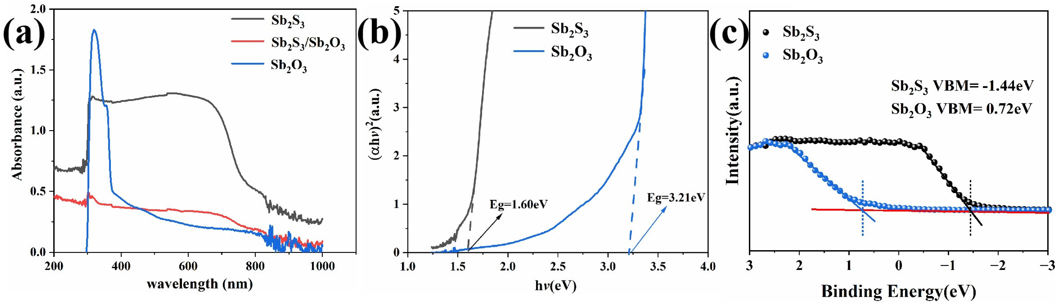
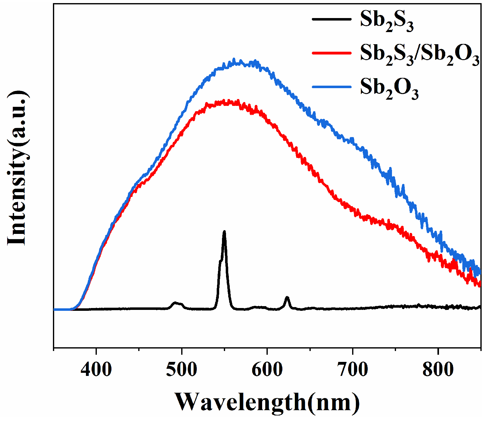
3.2. Analysis of Optical Properties of Sb2S3 and the Sb2S3/Sb2O3 Heterojunction

The UV–visible absorption spectra of the Sb2S3, Sb2O3, and Sb2S3/Sb2O3 samples were measured using an ultraviolet–visible spectrometer (UV-Vis) over the wavelength range of 190–1000 nm. As shown in Figure 7a, the Sb2S3 thin films demonstrate strong visible light absorption in the range of 300 to 700 nm. In contrast, the Sb2O3 thin films exhibit significant ultraviolet absorption but are less effective in utilizing visible light. Notably, the visible light absorption capability of the Sb2S3/Sb2O3 heterojunction is considerably reduced. This observation aligns with findings by Yao et al. [26], which indicated that a TiO2/Sb2O3 heterojunction possesses a weaker light-absorbing capacity compared to monomeric TiO2. This reduction in absorption may be attributed to the higher optical refractive index of Sb2O3, which results in a considerable portion of visible light being reflected, with only a small fraction absorbed by Sb2S3. Furthermore, analysis of the SEM images reveals that the decreased visible light absorption is likely due to the Sb2O3 particle morphology covering the surface of the Sb2S3 film, thereby obstructing light penetration and absorption.
The optical band gaps (Eg) of Sb2S3 and Sb2O3 were accurately calculated using Tauc plots as shown in Equation (2) [37]:
α h v n = A h v E g
where α is the optical absorption coefficient (cm−1), hν is the energy of the incident photon (eV), Eg is the Tauc’s bandgap (eV) of the sample, and the value of n depends on the energy band nature of the sample. In the Tauc plot, a linear region is typically observed, and the intersection of this linear section with the horizontal axis represents the optical band gap. As illustrated in Figure 7b, the optical band gaps (Eg) of Sb2S3 and Sb2O3 are approximately 1.60 eV and 3.21 eV, respectively. Additionally, the valence band maxima (VBM) of Sb2S3 and Sb2O3 were determined using high-resolution X-ray photoelectron spectroscopy (XPS). Figure 7c shows that the VBM of Sb2S3 is −1.44 eV, while that of Sb2O3 is 0.72 eV.
The intensity of the steady-state photoluminescence (PL) spectra is commonly employed to characterize the complexation of photogenerated electrons and holes; a higher intensity indicates a greater degree of carrier complexation. Figure 8 presents the PL spectra of Sb2S3 and the Sb2S3/Sb2O3 heterojunction, excited by a 320 nm laser. As shown in the figure, the PL spectrum of Sb2S3 exhibits characteristic peaks at 494 nm, 550 nm, and 623 nm. In contrast, the PL spectrum of Sb2O3 displays a characteristic peak at 550 nm. Similarly, the Sb2S3/Sb2O3 heterojunction shows a prominent peak only at 550 nm, which may originate from the fluorescence characteristic peaks of both Sb2S3 and Sb2O3 at this wavelength. Notably, the characteristic peaks of Sb2S3 at 494 nm and 623 nm are nearly undetectable in the Sb2S3/Sb2O3 heterojunction, indicating that their intensity is significantly lower than that observed for Sb2S3 alone. Thus, the Sb2S3/Sb2O3 heterojunction effectively suppresses carrier complexation [38].

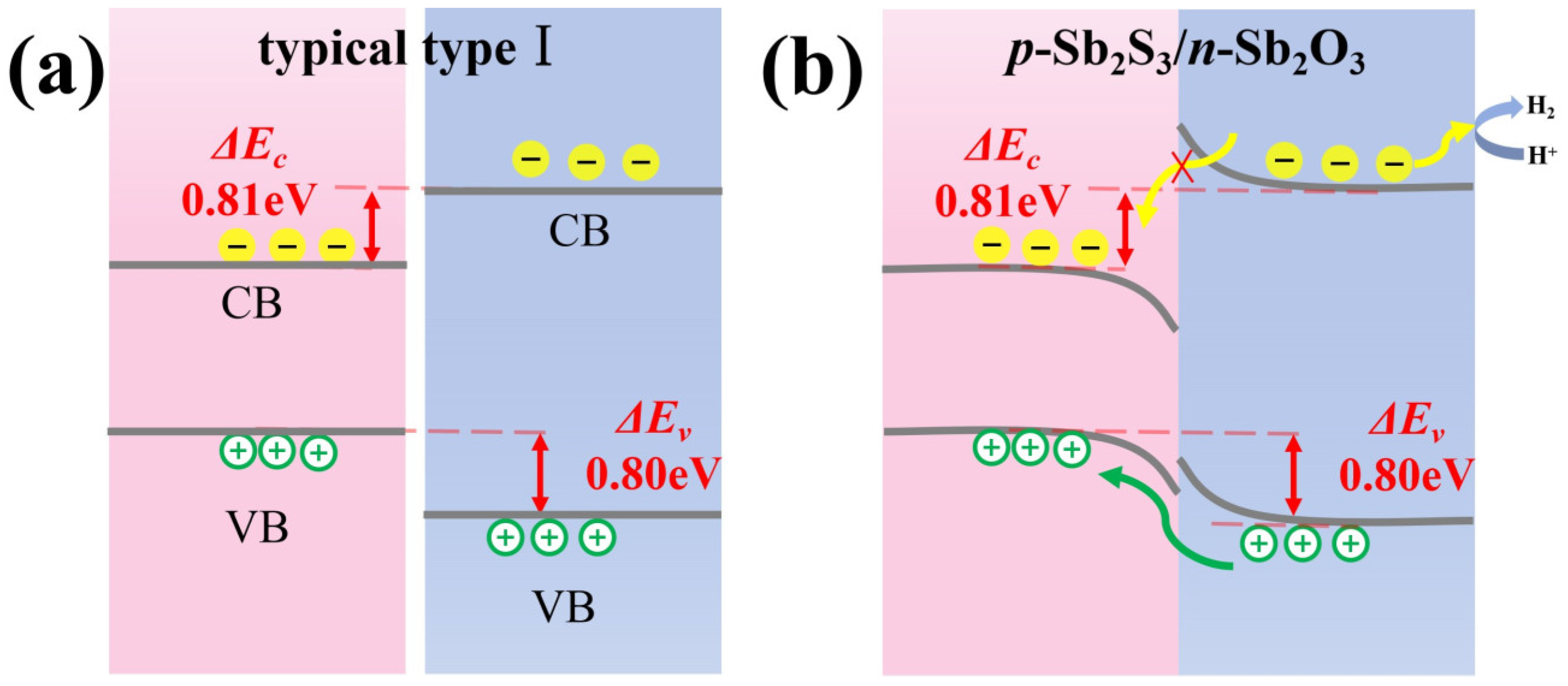
3.3. Schematic Diagram of the Energy Band of the Sb2S3/Sb2O3 Heterojunction

To ascertain the energy band alignment of the Sb2S3/Sb2O3 heterojunction and to construct an energy band diagram, high-resolution X-ray photoelectron spectroscopy (XPS) was utilized to measure the valence band maximum (VBM) positions for both Sb2S3 and Sb2O3. The VBM values for Sb2S3 and Sb2O3 were found to be −1.44 eV and 0.72 eV, respectively. Additionally, UV–visible spectroscopy inferred the optical band gaps (Eg) of Sb2S3 and Sb2O3 to be approximately 1.60 eV and 3.21 eV, respectively. Furthermore, the XPS results revealed the core energy levels of both Sb2S3 and Sb2O3. According to the Kraut method [39], the valence band offset (ΔEv) and the conduction band offset (ΔEc) of the Sb2S3/Sb2O3 heterojunction can be calculated using Equations (3) and (4) [35,40,41]:
E v = E S b   3 d 5 / 2 S b 2 S 3 E V B M S b 2 S 3 + E 1 S b   3 d 5 / 2 S b 2 S 3 / S b 2 O 3 E 2 S b   3 d 5 / 2 S b 2 S 3 / S b 2 O 3 E S b   3 d 5 / 2 S b 2 O 3 E V B M S b 2 O 3
E c = E g S b 2 S 3 + E v E g S b 2 O 3
In this context, E S b   3 d 5 / 2 S b 2 S 3 and E S b   3 d 5 / 2 S b 2 O 3 represent the core energy levels of Sb2S3 and Sb2O3, which are 527.45 eV and 529.59 eV, respectively; E 1 S b   3 d 5 / 2 S b 2 S 3 / S b 2 O 3 is the core energy level of the wide bandgap Sb2O3 in the Sb2S3/Sb2O3 heterojunction, at 529.45 eV; and E 2 S b   3 d 5 / 2 S b 2 S 3 / S b 2 O 3 is the core energy level of the narrow bandgap Sb2S3, at 528.67 eV. The calculated values for the valence band offset (ΔEv) and the conduction band offset (ΔEc) are 0.80 eV and −0.81 eV, respectively. Based on these band offsets, a schematic energy band diagram of the Sb2S3/Sb2O3 heterojunction is illustrated in Figure 9.
Figure 9a is a schematic energy band diagram of the Sb2S3/Sb2O3 heterojunction under dark conditions. Based on the valence band and conduction band offset energies, the Sb2S3/Sb2O3 heterojunction is classified as a Type I heterojunction. In a Type I heterojunction, photo-excited holes and electrons tend to transfer to the semiconductor with a narrower bandgap [40,42]. However, due to the changes in surface potential induced by illumination in semiconductors, the Surface Photovoltage (SPV) is defined as the change in surface potential caused by light exposure, which is used to characterize the separation of photo-generated charge carriers. The presence of a surface space charge region (SCR) resulting from the potential difference at the semiconductor surface typically leads to n-type semiconductors exhibiting a positive SPV, where the band edges of the SCR bend upward. Conversely, p-type semiconductors exhibit a negative SPV, with the band edges of the SCR bending downward [43]. Therefore, the band edges of Sb2S3 bend downward, while those of Sb2O3 bend upward. The bending of the valence band at the interface facilitates the transfer of photo-generated holes from Sb2O3 to the high valence band of Sb2S3. The potential barrier caused by the bending of the conduction band prevents the photo-generated electrons from Sb2O3 from moving to the conduction band side of Sb2S3 (Figure 9b). In this process, the photo-generated electrons from Sb2O3 can be retained in the conduction band with a higher reduction potential, participating in photocatalytic hydrogen evolution reactions, while the photo-generated holes transfer to the Sb2S3 side and move to the counter electrode under the influence of an external voltage to participate in oxygen evolution reactions. This special Type I heterostructure and band bending achieve the separation of photo-generated electron–hole pairs, enhancing the separation efficiency of photo-generated charge carriers.

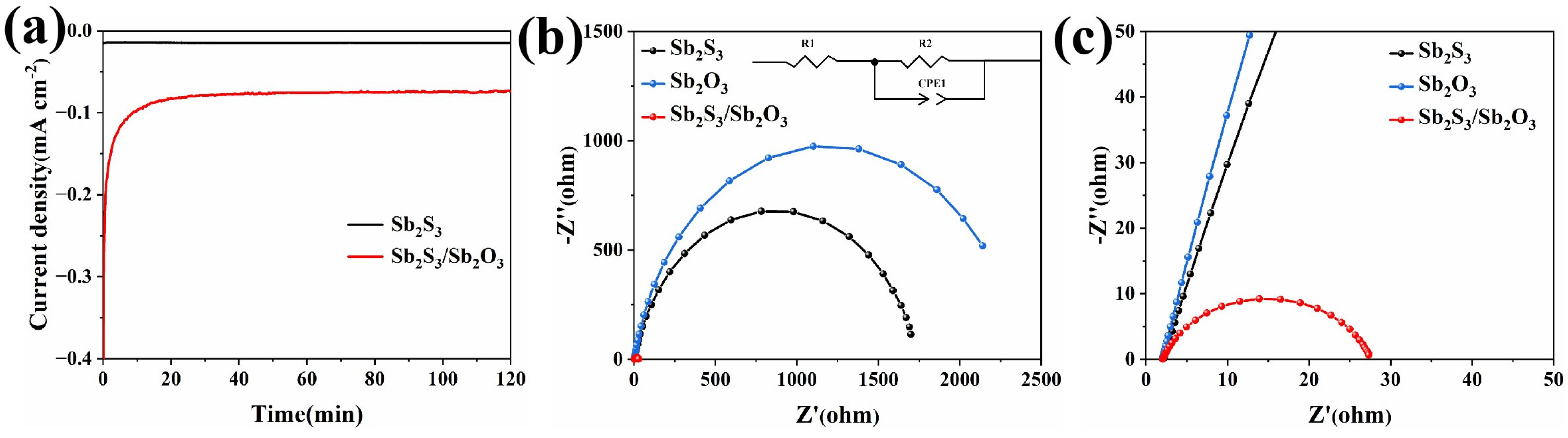
3.4. Photoelectrochemical Characterization of Sb2S3 and the Sb2S3/Sb2O3 Heterojunction

The transient photocurrent response (TPR) and electrochemical impedance (EIS) of a photocatalyst determine the intensity and migration efficiency of the material’s photogenerated carriers. The photogenerated electron–hole separation, migration efficiency, and stability of Sb2S3 and the Sb2S3/Sb2O3 heterojunction were tested using an electrochemical workstation coupled with a 300 W xenon lamp.
Figure 10 presents the linear scanning voltage (J-V) plots for both single Sb2S3 and the Sb2S3/Sb2O3 heterojunction, with applied bias voltages ranging from 0.45 V to −0.15 V (vs. RHE). The measurements were conducted with a 5 s on-time and off-time, at a sweep rate of 2 mV s−1. It was observed that both single Sb2S3 and the Sb2S3/Sb2O3 heterojunction generate photocurrents upon photoelectric excitation. Notably, the photocurrent response of the Sb2S3/Sb2O3 heterojunction is significantly greater than that of Sb2S3, indicating that the heterojunction is more effective in generating photogenerated carriers upon photoexcitation. The photocurrent density of the Sb2S3/Sb2O3 heterojunction consistently exceeds that of Sb2S3 across the range of applied bias voltages. For instance, at −0.15 V (vs. RHE), the photocurrent density reaches −0.056 mA cm−2, which is 1.40 times greater than that of Sb2S3, which has a photocurrent density of −0.040 mA cm−2. Furthermore, the photocurrent densities of the Sb2S3/Sb2O3 heterojunction are 3.28, 2.6, 1.88, 1.51, and 1.37 times higher than those of Sb2S3 at the applied bias voltages of 0.35 V, 0.25 V, 0.15 V, 0.05 V, and −0.05 V (vs. RHE), respectively.
Figure 11a illustrates the time–current (I-t) profiles for the monomer Sb2S3 and the Sb2S3/Sb2O3 heterojunction. These profiles were obtained to assess the stability of the photocathodes during an electrochemical process under continuous illumination at an applied bias voltage of −0.15 V (vs. RHE) for 2 h. The current density at the light state of Sb2S3 remains stable throughout the illumination period, showing little to no change, and stabilizes at −0.015 mA cm−2. Conversely, the current density at the light state of the Sb2S3/Sb2O3 heterojunction initially experiences a decline but stabilizes after approximately 20 min of illumination, maintaining a consistent value of −0.075 mA cm−2; this stabilized current is five times greater than that of Sb2S3.
Figure 11b presents the electrochemical impedance spectroscopy (EIS) patterns for Sb2S3, Sb2O3, and the Sb2S3/Sb2O3 heterojunction, which were evaluated under continuous illumination and an applied bias voltage of −0.15 V (vs. RHE). In this context, the diameter of the semicircle represents the charge transfer impedance (R2) at the electrode–electrolyte interface, while R1 corresponds to the solution resistance, and CPE1 represents the transfer capacitance. A smaller semicircle diameter in the electrochemical impedance spectroscopy (EIS) pattern indicates lower impedance and reduced charge transfer resistance at the electrode–electrolyte interface. The results reveal that the Sb2S3/Sb2O3 heterojunction has the smallest semicircle diameter (as shown in Figure 11c), suggesting the lowest charge transfer resistance and the highest charge migration efficiency. This finding further reinforces the idea that the formation of the Sb2S3/Sb2O3 heterojunction enhances the migration efficiency of photogenerated carriers.
The photocatalytic hydrogen evolution performance of the electrodes was characterized using a photocatalytic evaluation system. With an applied voltage of −0.15 V, the samples were illuminated for 60 min, and the hydrogen produced was automatically detected using a gas chromatograph. The temperature of the entire experimental system was maintained at 25 °C. First, hydrogen calibration was conducted, in which 1 mL of hydrogen was injected into the photocatalytic system, resulting in a chromatographic peak area of 40.8321 for the 1 mL of hydrogen, with a peak retention time of 2.093 min. Based on this data, the hydrogen evolution rates for both Sb2S3 and the Sb2S3/Sb2O3 heterojunction were calculated. It is clear from Figure 12 and Table 1 that the hydrogen precipitation rate of Sb2S3 is 0.081 mL cm−2 h−1, whereas that of the Sb2S3/Sb2O3 heterojunction is about twice that of Sb2S3. This difference is undoubtedly attributed to the significant improvement in photoelectrocatalytic performance of the Sb2S3/Sb2O3 heterojunction.

4. Conclusions

In summary, the Sb2S3/Sb2O3 heterojunction was successfully synthesized through the electrodeposition of a metallic Sb film, followed by vulcanization and chemical bath deposition. Characterization techniques, including X-ray diffraction (XRD), scanning electron microscopy (SEM), energy-dispersive spectroscopy (EDS), and X-ray photoelectron spectroscopy (XPS), confirmed the formation of the Sb2S3/Sb2O3 heterojunction, characterized by larger particles in the upper layer and a lamellar morphology in the lower layer. The calculation results obtained from the Kraut method indicate that the synthesized Sb2S3/Sb2O3 heterojunction is categorized as a Type I heterostructure. The unique characteristics of this Type I heterostructure and band bending facilitate the separation of photogenerated charge carriers. Under simulated sunlight, the Sb2S3/Sb2O3 heterojunction exhibited a photocurrent density of −0.056 mA cm−2 at −0.15 V, which is 1.40 times greater than that of monomeric Sb2S3. In the hydrogen precipitation experiment with a light time of 60 min, the hydrogen precipitation rate of the Sb2S3/Sb2O3 heterojunction is 0.163 mL cm−2 h−1, which is about twice that of Sb2S3. The mechanisms underlying the enhanced photocurrent were investigated using electrochemical impedance spectroscopy, steady-state fluorescence spectroscopy, and photoelectrochemical (PEC) measurements. The improved photoelectrochemical performance of the Sb2S3/Sb2O3 heterojunction can be attributed to a reduction in interfacial transport impedance and a significant increase in the efficiency of photogenerated carrier separation. The formation of a heterojunction between Sb2S3 and Sb2O3 effectively enhances the photoelectrochemical performance of the photoanode, addressing issues related to the separation efficiency of photogenerated carriers and the recombination rate in Sb2S3 films to some extent. Meanwhile, loading co-catalysts is an effective approach to improving the photoelectrochemical performance of photoanodes. In future studies, loading co-catalysts on the Sb2S3/Sb2O3 heterojunction is expected to further enhance its photoelectrochemical performance.

Author Contributions

Conceptualization, H.T. and J.Y.; methodology, H.T. and J.Y.; software, J.Y., B.X., S.L. and B.Y.; validation, H.T., J.Y., Z.C., R.T. and T.L.; formal analysis, H.T., Z.C., R.T. and T.L.; investigation, H.T., Z.C., R.T. and T.L.; resources, J.Y., B.X., S.L. and B.Y.; data curation, H.T., Z.C., R.T. and T.L.; writing—original draft, H.T., Z.C., R.T. and T.L.; writing—review and editing, J.Y., B.X., S.L. and B.Y.; visualization, H.T., Z.C., R.T. and T.L.; supervision, J.Y., B.X., S.L. and B.Y.; project administration, J.Y., B.X., S.L. and B.Y.; funding acquisition, J.Y., B.X., S.L. and B.Y. All authors have read and agreed to the published version of the manuscript.

Funding

This research was funded by [National Natural Science Foundation of China] grant number [52264038, 52474329, and 52104350], [the Natural Science Foundation of Yunnan Province] grant number [No. 202401AT070397], [the National Key Research and Development Program of China] grant number [2022YFC2904204] And The APC was funded by [National Natural Science Foundation of China].

Data Availability Statement

No new data were created. Requests for data related to the research results may be directed to the corresponding author and will be available upon reasonable request.

Acknowledgments

In the course of my research and writing of this thesis, I received support and assistance from many individuals, as well as financial backing. Here, I would like to express my sincere gratitude to them.

Conflicts of Interest

The authors declare that they have no known competing financial interests or personal relationships that could have appeared to influence the work reported in this paper.

References

  1. Yang, L.; Li, F.; Xiang, Q. Advances and challenges in the modification of photoelectrode materials for photoelectrocatalytic water splitting. Mater. Horiz. 2024, 11, 1638–1657. [Google Scholar] [CrossRef] [PubMed]
  2. Suri, D.; Das, S.; Choudhary, S.; Venkanna, G.; Sharma, B.; Afroz, M.A.; Tailor, N.K.; Joshi, R.; Satapathi, S.; Tripathi, K. Enigma of Sustainable CO2 Conversion to Renewable Fuels and Chemicals Through Photocatalysis, Electrocatalysis, and Photoelectrocatalysis: Design Strategies and Atomic Level Insights. Small 2025, 21, 2408981. [Google Scholar] [CrossRef] [PubMed]
  3. Li, S.-Y.; Huang, K.F.; Tang, Z.Y.; Wang, J.H. Photoelectrocatalytic organic synthesis: A versatile method for the green production of building-block chemicals. J. Mater. Chem. A 2023, 11, 3281–3296. [Google Scholar] [CrossRef]
  4. Le, P.-A.; Trung, V.D.; Nguyen, P.L.; Bac Phung, T.V.; Natsuki, J.; Natsuki, T. The current status of hydrogen energy: An overview. RSC Adv. 2023, 13, 28262–28287. [Google Scholar] [CrossRef]
  5. Fu, W.; Zhang, Y.; Zhang, X.; Yang, H.; Xie, R.; Zhang, S.; Lv, Y.; Xiong, L. Progress in Promising Semiconductor Materials for Efficient Photoelectrocatalytic Hydrogen Production. Molecules 2024, 29, 289. [Google Scholar] [CrossRef]
  6. Fujishima, A.; Honda, K. Electrochemical Photolysis of Water at a Semiconductor Electrode. Nature 1972, 238, 37–38. [Google Scholar] [CrossRef]
  7. Lu, Y.; Wang, Z.; Su, J. Sb2S3 surface modification for improved photoelectrochemical water splitting performance of BiVO4 photoanode. J. Photonics Energy 2021, 11, 016502. [Google Scholar] [CrossRef]
  8. Xu, Y.; Schoonen MA, A. The absolute energy positions of conduction and valence bands of selected semiconducting minerals. Am. Mineral. 2000, 85, 543–556. [Google Scholar] [CrossRef]
  9. Kondrotas, R.; Chen, C.; Tang, J. Sb2S3 Solar Cells. Joule 2018, 2, 857–878. [Google Scholar] [CrossRef]
  10. Shah, U.A.; Chen, S.; Khalaf, G.M.G.; Jin, Z.; Song, H. Wide Bandgap Sb2S3 Solar Cells. Adv. Funct. Mater. 2021, 31, 2100265. [Google Scholar] [CrossRef]
  11. Myagmarsereejid, P.; Ingram, M.; Batmunkh, M.; Zhong, Y.L. Doping Strategies in Sb2S3 Thin Films for Solar Cells. Small 2021, 17, 2100241. [Google Scholar] [CrossRef] [PubMed]
  12. Kang, Y.; Deng, H.; Wu, K.; Wang, G.; Hong, J.; Wang, W.; Wu, J.; Zhou, H.; Xia, Y.; Cheng, S. Self-powered Sb2S3 photodetectors with efficient carrier transport enabled by compact vertical TiO2 nanorods. Opt. Lett. 2024, 49, 6533–6536. [Google Scholar] [CrossRef] [PubMed]
  13. Fu, S.; Liu, X.; Man, J.; Ou, Q.; Zheng, X.; Liu, Z.; Zhu, T.; Wang, H.E. 2D/1D PbI2/Sb2S3 van der Waals heterojunction for highly sensitive and broadband photodetectors. J. Mater. Chem. C 2024, 12, 3353–3364. [Google Scholar] [CrossRef]
  14. Lian, X.; Li, S.; Jiang, J.; Huang, W.; He, N.; Liu, X.; Wu, J.; Wang, Z.; Zhu, G.; Wang, L. Plasmonically-enhanced reconfigurable photodetector based on graphene/Sb2S3 heterojunction. Appl. Phys. Express 2025, 18, 015003. [Google Scholar] [CrossRef]
  15. Ijaz, M.; Shahzad Ahmad, K.; Nawaz, F.; Makawana, B.; Gupta, R.K.; Abdel-Maksoud, M.A.; Al-Qahtani, W.H.; Malik, A. Nanocomposite Material Sb2S3:SnS:MnS2 its Fabrication and Utilization as Efficient Electrode for Energy Storage in Supercapacitor. ChemistrySelect 2024, 9, e202403513. [Google Scholar] [CrossRef]
  16. Jaffri, S.B.; Ahmad, K.S.; Al-Hawadi, J.S.; Panchal, H.; Gupta, R.K.; Ashraf, G.A.; Okla, M.K. Harnessing sustainable energy: Synthesizing a trinary chalcogenide semiconductor BaS:Sb2S3:CuS for enhanced performance in supercapacitor devices and electro-catalysis. J. Energy Storage 2024, 103, 114527. [Google Scholar] [CrossRef]
  17. Wang, Y.; Jin, M.; Wan, Z.; Chen, C.; Cao, W.; Naveed, F.; Kuang, J.; Cheng, L.; Lei, L.; Chen, J.; et al. PbSe-Induced Sb2S3 Crystallization and Interface Band Optimization for High-Efficiency Bulk Heterojunction Sb2S3 Solar Cells. Adv. Funct. Mater. 2025, 23, 2420361. [Google Scholar] [CrossRef]
  18. Kumar, P.; Thomas, J.P.; Kharytonau, D.S.; Gradone, A.; Gilli, N.; You, S.; Leung, K.T.; Morandi, V.; Vomiero, A. Cadmium-free electron transport layers for hydrothermally processed semitransparent Sb2S3 solar cells. Nano Energy 2025, 134, 110539. [Google Scholar] [CrossRef]
  19. Hou, S.; Zhang, X.; Dai, G.; Wang, X.; Wang, H.; Chen, T.; Wang, K.; Xiao, X.; Li, J. Surface treatment processed electron transport layers for efficient Sb2S3 solar cells. Chem. Eng. J. 2024, 500, 156907. [Google Scholar] [CrossRef]
  20. Chihi, A. Synthesis of Sb2S3:Eu thin films as a catalyst for the efficient photocatalytic degradation of rhodamine B (RhB) dye under visible light. RSC Adv. 2025, 15, 5681–5697. [Google Scholar] [CrossRef]
  21. Tian, L.; Li, J.; Wang, J.; Yang, Z.; Li, Y.; Zhang, L.; Zhang, G. Built-in electric field intensified by SPR effect to drive charge separation over Ag-AgI/Sb2S3 heterojunction for high-efficiency photocatalytic metronidazole mineralization. Sep. Purif. Technol. 2024, 346, 127443. [Google Scholar] [CrossRef]
  22. Farhana, M.A.; Manjceevan, A.; Bandara, J. Recent advances and new research trends in Sb2S3 thin film based solar cells. J. Sci.Adv. Mater. Devices 2023, 8, 100533. [Google Scholar] [CrossRef]
  23. Zhang, J.; Liu, Z.; Liu, Z. Novel WO3/Sb2S3 Heterojunction Photocatalyst Based on WO3 of Different Morphologies for Enhanced Efficiency in Photoelectrochemical Water Splitting. ACS Appl. Mater. Interfaces 2016, 8, 9684–9691. [Google Scholar] [CrossRef] [PubMed]
  24. Kılıç, Ç.; Zunger, A. n-type doping of oxides by hydrogen. Appl. Phys. Lett. 2002, 81, 73–75. [Google Scholar] [CrossRef]
  25. Tigau, N. Structure and electrical conduction of Sb2O3 thin films. Cryst. Res. Technol. 2006, 41, 1106–1111. [Google Scholar] [CrossRef]
  26. Yao, X.; Zuo, J.; Wang, Y.-J.; Song, N.-N.; Li, H.-H.; Qiu, K. Enhanced Photocatalytic Degradation of Perfluorooctanoic Acid by Mesoporous Sb2O3/TiO2 Heterojunctions. Front. Chem. 2021, 9, 690520. [Google Scholar] [CrossRef]
  27. Nalina, M.; Messaddeqa, Y.; Ribeiroa, S.; Poulainb, M.; Briois, V.; Sud, P. Photosensitivity in Antimony Based Glasses. J. Optoelectron. Adv. Mater. 2001, 3, 553–558. [Google Scholar]
  28. Cao, G.; Su, J.; Lu, J.; Zhang, J.; Liu, Q. Preparation of Sb2O3-loaded Activated Carbon Particle Electrode and Its Electrocatalytic Degradation of Methyl Orange in a Three-dimensional Electrode Cell. J. Chin. Chem. Soc. 2012, 59, 583–588. [Google Scholar] [CrossRef]
  29. Li, X.; Wang, X.; Ning, X.; Lei, J.; Shao, J.; Wang, W.; Huang, Y.; Hou, B. Sb2S3/Sb2O3 modified TiO2 photoanode for photocathodic protection of 304 stainless steel under visible light. Appl. Surf. Sci. 2018, 462, 155–163. [Google Scholar] [CrossRef]
  30. Jiang, L.; Chen, J.; Wang, Y.; Pan, Y.; Xiao, B.; Ouyang, N.; Liu, F. Sb2O3/Sb2S3 Heterojunction Composite Thin Film Photoanode Prepared via Chemical Bath Deposition and Post-Sulfidation. J. Electrochem. Soc. 2018, 165, H1052–H1058. [Google Scholar] [CrossRef]
  31. Prabhakar, R.R.; Moehl, T.; Siol, S.; Suh, J.; Tilley, S.D. Sb2S3/TiO2 Heterojunction Photocathodes: Band Alignment and Water Splitting Properties. Chem. Mater. 2020, 32, 7247–7253. [Google Scholar] [CrossRef]
  32. Prabhakar, R.R.; Septina, W.; Siol, S.; Moehl, T.; Wick-Joliat, R.; Tilley, S.D. Photocorrosion-resistant Sb2Se3 photocathodes with earth abundant MoSx hydrogen evolution catalyst. J. Mater. Chem. A 2017, 5, 23139–23145. [Google Scholar] [CrossRef]
  33. Wang, Y.; Jiang, L.; Liu, Y.; Tang, D.; Liu, F.; Lai, Y. Facile synthesis and photoelectrochemical characterization of Sb2O3 nanoprism arrays. J. Alloy. Compd. 2017, 727, 469–474. [Google Scholar] [CrossRef]
  34. Song, D.; Liu, Y.; Sun, C.; Zhao, Y.; Zhu, T.; Yang, R.; Song, Y.; Zhao, J. Designed composite catalysts of Cu-doped BiOCl nanosheets on CuFe-PBA cubes for enhanced photoelectrochemical H2 evolution activity in neutral medium. Colloids Surf. A Physicochem. Eng. Asp. 2023, 679, 132592. [Google Scholar] [CrossRef]
  35. Han, T.; Luo, M.; Liu, Y.; Lu, C.; Ge, Y.; Xue, X.; Dong, W.; Huang, Y.; Zhou, Y.; Xu, X. Sb2S3/Sb2Se3 heterojunction for high-performance photodetection and hydrogen production. J. Colloid Interface Sci. 2022, 628, 886–895. [Google Scholar] [CrossRef]
  36. Zhang, L.; Xin, C.; Jin, W.; Sun, Q.; Wang, Y.; Wang, J.; Hu, X.; Miao, H. Novel Sb2S3-xSex photocathode decorated NiFe-LDH hole blocking layer with enhanced photoelectrochemical performance. Appl. Surf. Sci. 2023, 639, 158184. [Google Scholar] [CrossRef]
  37. Klein, J.; Kampermann, L.; Mockenhaupt, B.; Behrens, M.; Strunk, J.; Bacher, G. Limitations of the Tauc Plot Method. Adv. Funct. Mater. 2023, 33, 2304523. [Google Scholar] [CrossRef]
  38. Ma, Z.; Yang, Y.; Wei, X.; Li, Q.; Zhang, D.; Wang, Y.; Liu, E.; Miao, H. CdSe Quantum Dots Supported on Sb2S3 Nanorods as S-Scheme Heterojunction Photoanode in Photoelectrochemical Cells. ACS Appl. Nano Mater. 2024, 7, 24213–24223. [Google Scholar] [CrossRef]
  39. Kraut, E.A.; Grant, R.W.; Waldrop, J.R.; Kowalczyk, S.P. Precise Determination of the Valence-Band Edge in X-Ray Photoemission Spectra: Application to Measurement of Semiconductor Interface Potentials. Phys. Rev. Lett. 1980, 44, 1620–1623. [Google Scholar] [CrossRef]
  40. Luo, M.; Lu, C.; Liu, Y.; Han, T.; Ge, Y.; Zhou, Y.; Xu, X. Band alignment of type-I SnS2/Bi2Se3 and type-II SnS2/Bi2Te3 van der Waals heterostructures for highly enhanced photoelectric responses. Sci. China Mater. 2022, 65, 1000–1011. [Google Scholar] [CrossRef]
  41. Tangi, M.; Mishra, P.; Tseng, C.-C.; Ng, T.K.; Hedhili, M.N.; Anjum, D.H.; Alias, M.S.; Wei, N.; Li, L.-J.; Ooi, B.S. Band Alignment at GaN/Single-Layer WSe2 Interface. ACS Appl. Mater. Interfaces 2017, 9, 9110–9117. [Google Scholar] [CrossRef] [PubMed]
  42. Ho, T.A.; Bae, C.; Joe, J.; Yang, H.; Kim, S.; Park, J.H.; Shin, H. Heterojunction Photoanode of Atomic-Layer-Deposited MoS2 on Single-Crystalline CdS Nanorod Arrays. ACS Appl. Mater. Interfaces 2019, 11, 37586–37594. [Google Scholar] [CrossRef] [PubMed]
  43. Jia, X.; Lu, Y.; Du, K.; Zheng, H.; Mao, L.; Li, H.; Ma, Z.; Wang, R.; Zhang, J. Interfacial Mediation by Sn And S Vacancies of p—SnS/n—ZnIn2S4 for Enhancing Photocatalytic Hydrogen Evolution with New Scheme of Type—I Heterojunction. Adv. Funct. Mater. 2023, 33, 2304072. [Google Scholar] [CrossRef]
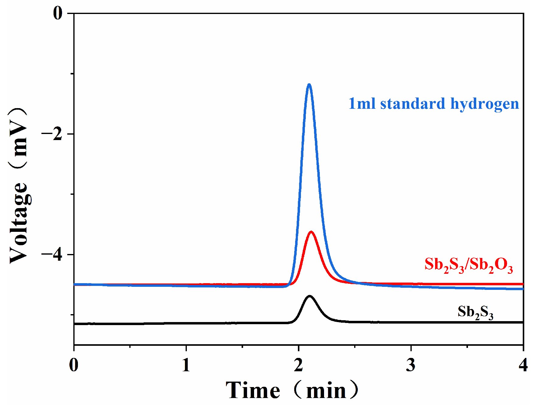
Figure 1. XRD patterns of Sb2S3 and the Sb2S3/Sb2O3 heterojunction.
Metals 15 00478 g001
Figure 2. Surface SEM patterns of Sb2S3 (a), Sb2O3 (b), and the Sb2S3/Sb2O3 (c) heterojunction.
Metals 15 00478 g002
Figure 3. Surface EDS patterns and elemental mapping of Sb2S3 (a), Sb2O3 (b), and the Sb2S3/Sb2O3 heterojunction (c).
Metals 15 00478 g003
Figure 4. EDS spectra and compositional data for Sb2S3, Sb2O3, and the Sb2S3/Sb2O3 heterojunction.
Metals 15 00478 g004
Figure 5. Cross-sectional morphology of Sb2S3 (a), Sb2O3 (b), and the Sb2S3/Sb2O3 heterojunction (c).
Metals 15 00478 g005
Figure 6. (a) Full scan XPS spectra of Sb2S3, Sb2O3, and the Sb2S3/Sb2O3 heterojunction. (b) XPS signals of Sb from Sb2S3, Sb2O3, and the Sb2S3/Sb2O3 heterojunction.
Metals 15 00478 g006
Figure 7. (a) UV-Vis absorption spectra of Sb2S3, Sb2O3, and the Sb2S3/Sb2O3 heterojunction. (b) Tauc plots for Sb2S3 and Sb2O3. (c) Valence band spectra of Sb2S3 and Sb2O3.
Metals 15 00478 g007
Figure 8. PL spectra of Sb2S3, Sb2O3, and the Sb2S3/Sb2O3 heterojunction (λex = 320 nm).
Metals 15 00478 g008
Figure 9. Schematic band diagrams of Sb2S3 and Sb2O3 before (a) and after (b) heterojunction.
Metals 15 00478 g009
Figure 10. Linear scanning voltammetry curves (a), and the photocurrent density values (b) of Sb2S3 and the Sb2S3/Sb2O3 heterojunction.
Metals 15 00478 g010
Figure 11. Time–current curves of Sb2S3 and Sb2S3/Sb2O3 heterojunctions (a), EIS impedance plots, (b) and localized EIS impedance magnification (c).
Metals 15 00478 g011
Figure 12. Hydrogen precipitation curves of the 1 mL standard hydrogen peak, Sb2S3, and the Sb2S3/Sb2O3 heterojunction after 60 min of light exposure.
Metals 15 00478 g012
Table 1. Hydrogen precipitation volume and rate of hydrogen precipitation from Sb2S3 and the Sb2S3/Sb2O3 heterojunction after 60 min of illumination.
SampleTime of Appearance of Hydrogen PeakChromatographic Peak AreaHydrogen Volume/mLHydrogen Precipitation rate/mL cm−2 h−1
1 mL standard hydrogen2.03940.83211.000\
Sb2S32.0984.98910.1220.081
Sb2S3/Sb2O32.1119.94380.2440.163
Disclaimer/Publisher’s Note: The statements, opinions and data contained in all publications are solely those of the individual author(s) and contributor(s) and not of MDPI and/or the editor(s). MDPI and/or the editor(s) disclaim responsibility for any injury to people or property resulting from any ideas, methods, instructions or products referred to in the content.

