Article

Irradiation Hardening and Microstructure Study of MAX-Phase-Dispersion-Strengthened Vanadium Alloy under Self-Ion Irradiation

1
Southwestern Institute of Physics, Chengdu 610041, China
2
Key Laboratory of Artificial Micro- and Nano-Structures of Ministry of Education, Hubei Nuclear Solid Physics Key Laboratory, School of Physics and Technology, Wuhan University, Wuhan 430072, China
3
College of Science, Dalian Maritime University, Dalian 116026, China
*
Authors to whom correspondence should be addressed.
Metals 2024, 14(2), 141; https://doi.org/10.3390/met14020141
Submission received: 11 December 2023 / Revised: 16 January 2024 / Accepted: 19 January 2024 / Published: 24 January 2024
(This article belongs to the Special Issue Radiation Damage in Metallic Systems for Fusion Energy Applications)

Abstract

:
V-4Cr-4Ti alloy is one of the candidate structural materials for future fusion reactors due to its desirable characteristics. In our previous research, MAX-phase-dispersion-strengthened vanadium alloy (V-4Cr-4Ti-1.5Y-0.3Ti3SiC2), prepared through mechanical alloying, showed excellent thermal stability and creep resistance and was expected to have good radiation resistance. This study investigates the effects of 2.5 MeV V2+ ion irradiation on V-4Cr-4Ti-1.5Y-0.3Ti3SiC2 and V-4Cr-4Ti alloys at 500 °C, with peak damage of 0.8, 3.5, and 6.1 dpa. Transmission electron microscopy and nanoindentation were used to examine the changes in microstructure and hardness before and after irradiation. The microscopic analysis reveals that dispersed nanoparticles maintained good stability under irradiation. Defect clusters grow with increasing irradiation doses in both materials. The nanoindentation results show that V-4Cr-4Ti-1.5Y-0.3Ti3SiC2 has higher initial hardness and lower irradiation hardening, indicating better resistance to radiation hardening than V-4Cr-4Ti. This research serves as a valuable reference for the assessment of the irradiation resistance of Ti3SiC2-dispersion-strengthened V-4Cr-4Ti alloy.

1. Introduction

Vanadium alloy is one of the candidate structural materials for future fusion reactors due to its low neutron irradiation activation, non-ferromagnetism, excellent high-temperature strength, and good compatibility with liquid coolant lithium [1]. Nowadays, further strengthening of alloys has become a major focus of research. In this context, oxide dispersion strengthening technology has received increasing attention as a method for further enhancing the high-temperature performance of alloys [2,3]. Studies have shown that it can significantly enhance the operating temperature, mechanical properties, and radiation resistance of vanadium alloy, leading to an extension of service life [4,5,6]. Due to the special environment of liquid Li in which vanadium alloys will operate, and the greater affinity of vanadium alloys for C compared to O in liquid Li environments, carbides are more suitable for dispersion strengthening of vanadium alloys [7,8,9]. Recent studies have confirmed that introducing binary carbide TiC through mechanical alloying can effectively strengthen the vanadium alloy, improving its creep performance at high temperatures [10,11]. The MAX phase is a ternary layered ceramic with carbon or nitrogen as the key elements, and based on its excellent chemical stability [12,13,14,15,16], our group introduced MAX phase, “Ti3SiC2” nanoparticles, for the dispersion strengthening of the V-4Cr-4Ti alloy by mechanical alloying. Y is also added to reduce impurity elements such as O in the matrix [17,18]. Furthermore, the addition of Y can also enhance mechanical performance and reduce irradiation hardening [19,20,21]. Prior research reveals that a V-4Cr-4Ti alloy with “Y + Ti3SiC2” has a higher hardness after annealing at various high temperatures when compared to an alloy with “Y + TiC” and “Y + SiC”, demonstrating the exceptional thermal stability of this dispersion strengthening phase [22].
Vanadium alloy undergoes long-term high-energy neutron irradiation during service, resulting in the generation of a large number of point defects, such as interstitial atoms and vacancies. The aggregation of these point defects leads to the formation of dislocation loops, voids, and other defects, resulting in material swelling and hardening. These irradiation effects shorten the material’s service life and even jeopardize the safe operation of fusion reactors. Therefore, a comprehensive understanding of irradiation damage to MAX-phase-strengthened vanadium alloys is essential. Ion irradiation is commonly used to simulate neutron irradiation due to the disadvantages of neutron irradiation, such as the long experimental period, high price, and radioactivity of irradiated samples. Previous studies indicate that the dispersion of Ti3SiC2 can effectively strengthen vanadium alloy, improving thermal stability and creep resistance. However, comprehensive studies on the irradiation damage of Ti3SiC2-strengthened vanadium alloys are still lacking. A study by Y.F. Zhang et al. [23] has demonstrated that the irradiation hardening of the V-4Cr-4Ti-1.8Y-0.4Ti3SiC2 alloy is significantly lower than that of V-4Cr-4Ti under deuterium ion irradiation. This study provides a valuable reference for the strong radiation resistance of Ti3SiC2-strengthened vanadium alloys. However, deuterium ion implantation may introduce impurities, potentially influencing the comprehensive performance test results.
In order to study the effect of greater irradiation damage on the materials without introducing impurity elements, V-4Cr-4Ti-1.5Y-0.3Ti3SiC2 and V-4Cr-4Ti were irradiated with 2.5 MeV V2+ self-ions at 500 °C. To ensure the study of hardness and microstructure was as continuous as possible, the irradiation fluences were set to 1 × 10¹⁵, 4 × 10¹⁵, and 7 × 10¹⁵ ions cm−2 (corresponding to peak damage obtained at 900 nm depths of 0.8, 3.5, and 6.1 dpa, respectively). The microstructure and hardness variations of the two materials under different levels of irradiation damage were studied using transmission electron microscopy and nanoindentation techniques, and the possible mechanism of the experimental phenomenon was explained.

2. Materials and Methods

2.1. Sample Preparation

The purity and size of the initial powder were as follows: V, Cr, and Ti were 99.95% and 300 mesh, respectively; Y was 99.99% and 325 mesh; Ti3SiC2 was 99.5% and 200 mesh. These powders were then mixed to yield the compositions of V-4Cr-4Ti-1.5Y-0.3Ti3SiC2 in an argon atmosphere (99.9999%). A Retsch PM 400 mill (Retsch, Haan, Germany) was used as the MA equipment, with the MA vessels and balls made of WC/Co. The ball-to-material weight ratio was 5:1, and the total milling time was 140 h at a rotation speed of 170 rpm. Subsequently, the powders were canned in steel capsules, and hot isostatic pressing (HIPing) was applied at 150 MPa pressure in an argon atmosphere at 1050 °C for 3 h. The samples were then annealed at 750 °C for 5 h to eliminate residual stress. The V-4Cr-4Ti sample was a high-purity vanadium alloy smelted using an electron beam and annealed at 750 °C for 5 h to achieve the same experimental conditions. The V-4Cr-4Ti-1.5Y-0.3Ti3SiC2 and V-4Cr-4Ti samples were cut into sheets of 3 mm × 3 mm × 1 mm. The samples were first roughly polished with 400 #, 800 #, 1000 #, 2000 #, and 3000 # silicon carbide (SiC) paper successively and then finished with 1 # and 0.5 # grinding paste successively. Finally, they were electrochemically polished with 25% sulfuric acid and 75% ethanol polishing solution (in volume percent) at room temperature at a voltage of 10V for 60 s.

2.2. Self-Ion Irradiation

Ion-irradiation experiments were performed with 2.5 MeV V2+ ions at 500 °C using the 2 × 1.7 MV tandem accelerator in the Accelerator Laboratory of Wuhan University. Specific irradiation procedures and instruments can be found in the reference [24]. The irradiation fluences were 1 × 10¹⁵ ions cm−2, 4 × 10¹⁵ ions cm−2, and 8 × 10¹⁵ ions cm−2, and the irradiation time was 1.5 h, 6 h, and 10.5 h respectively. The vacuum degree was kept at 2.2 × 10⁻⁴ Pa, and the temperature error was kept at ±5 °C during the irradiation. According to the SRIM2013 “Rapid Calculation of Ion Distribution and Damage” model, the peak damage was about 0.8, 3.5, and 6.1 dpa (corresponding to 900 nm from the surface), respectively, and the displacement threshold energies of V, Cr, and Ti were 40 eV, 40 eV, and 30 eV, respectively [23]. At the peak of the damage (900 nm), the damage dose rate was about 1.6 × 10⁻⁴ dpa/s. The corresponding SRIM calculation results are shown in Figure 1, and the experimental conditions are shown in Table 1 below.
It is important to note that, in order to achieve the same irradiation dose, the temperature for ion irradiation will need to be higher than that for neutron irradiation due to the significantly larger dose rate associated with ion irradiation. For a given change in dose rate, we can obtain the shift in temperature required at a constant dose to keep the number of defects absorbed at sinks invariant according to Equation (1) [25].
T i T n = k T n 2 E v m ln ( G i G n ) 1 K T n E v m ln ( G i G n )
where k is Boltzmann’s constant and  E v m  is the vacancy migration energy. For vanadium alloy,  E v m   = 0.75 eV [26]. Ti is the ion irradiation temperature chosen for our experiment (773 K), and Tn is the neutron irradiation temperature corresponding to Ti when the dose is kept constant. Gi and Gn correspond to point defect generation rates for ion and neutron irradiation, respectively, and Gi/Gn represents the ratio of ion and neutron irradiation dose rates. According to Equation (1), one can obtain the temperature shift from the 773 K required at a constant dose in order to maintain the same point defect absorption at the sinks as a function of the ratio of dose rates as shown in Figure 1b. The dose rate of our experiment is about 3–4 orders of magnitude larger than the neutron irradiation dose rate of the fusion reactor [27]. Figure 1b shows that when the ion irradiation dose rate is 1000 to 10,000 times greater than that of neutron irradiation, the corresponding neutron irradiation temperature is about 480–425 K (207–152 °C). The optimal irradiation temperature for studying irradiation hardening and the evolution of defects such as dislocation loops in vanadium alloys is considered to be less than 0.4 Tm [27], where Tm represents the melting point of the vanadium alloy, estimated at about 1890 °C. Additionally, vanadium alloys are widely recognized to exhibit significant irradiation hardening at neutron irradiation temperatures below 400 °C. Hence, selecting 500 °C as the ion irradiation temperature is reasonable for studying irradiation hardening and the evolution of irradiation defects.

2.3. TEM Observation

The irradiated samples were prepared using the focused ion beam (FIB) method, which was performed with Scios 2 Dual Beam (Thermo Fisher Scientific, Waltham, MA, USA). The process began with the deposition of a Pt film in the selected area, followed by the use of a 30 keV Ga+ beam to groove the deposited area. Subsequently, the 2 µm thin sheet was then cut from the samples and attached to the TEM grid. Through a series of lower-energy ion beams, the thin layer was reduced to a thickness of 100 nm. A final step involved cleaning the sample with a 2 keV Ga+ beam to minimize the FIB defects. The size of FIB samples in this experiment was 4 µm × 4 µm. All FIB samples were observed using a JEM-2100 transmission electron microscope (JEOL, Tokyo, Japan) at the Wuhan University Analysis and Testing Center.

2.4. Nanoindentation Test

A nanoindentation test was performed using the Nano Indenter*G200 (Agilent Technologies, Santa Clara, CA, USA). The continuous stiffness measurement (CSM) mode was used to obtain the continuous curve of nanoindentation hardness (HIT) relative to indentation depth (nm). The indentation depth was set as 1200 nm, the strain rate was set as 0.05 s−1, the test temperature was room temperature (25 °C), and a minimum of 10 indentation points per sample were tested. The surface roughness of the sample greatly impacts the results of the nanoindentation test. Therefore, a flat and smooth area was manually selected for the indentation test. In order to avoid the interaction between different indentations, the distance between indentations was greater than 50 µm.

3. Results

3.1. TEM Observation of Microstructure

3.1.1. Nanoparticles in V-4Cr-4Ti-1.5Y-0.3Ti3SiC2

TEM observations were performed on the unirradiated region and “Y + MAX-0.8 dpa”, “Y + MAX-3.5 dpa”, and “Y + MAX-6.1 dpa” samples of V-4Cr-4Ti-1.5Y-0.3Ti3SiC2, as depicted in Figure 2a1–d1. The observations revealed the presence of irregularly shaped nanoparticles with a dispersed distribution within the sample, and the typical small-sized nanoparticles are highlighted in red circles. In a previous study by our group, the small nanoparticles were identified as Y2O3 and Ti3SiC2 using high-resolution transmission electron microscopy, with the possibility of the presence of a small amount of large-size TiC [22]. The number density and size of nanoparticles in both the unirradiated area and the region with peak damage depth (600–800 nm) at three irradiation doses were counted. For each sample, at least three regions measuring 300 nm × 300 nm × 100 nm were selected for statistical analysis. The statistical results revealed that the number density of nanoparticles in the unirradiated area was approximately 8.2 × 10²¹ m−3, with an average size of about 15.4 nm. Similarly, the “Y + MAX-0.8 dpa”, “Y + MAX-3.5 dpa”, and “Y + MAX-6.1 dpa” samples exhibited number densities of 7.9 × 10²¹ m−3, 8.1 × 10²¹ m−3, and 7.7 × 10²¹ m−3, with average sizes of 13.6 nm, 14.8 nm, and 14.3 nm, respectively. To ensure accuracy, only nanoparticles larger than 5 nm were counted, excluding the effects of black spot defects caused by FIB and small-size dislocation loops due to irradiation. Figure 2a2–d2 show the size distribution of nanoparticles. As can be seen from Figure 2a2–d2, all samples predominantly featured small-sized nanoparticles below 15 nm, and no significant differences were observed in size distribution at different irradiation doses.

3.1.2. Irradiation-Induced Defects

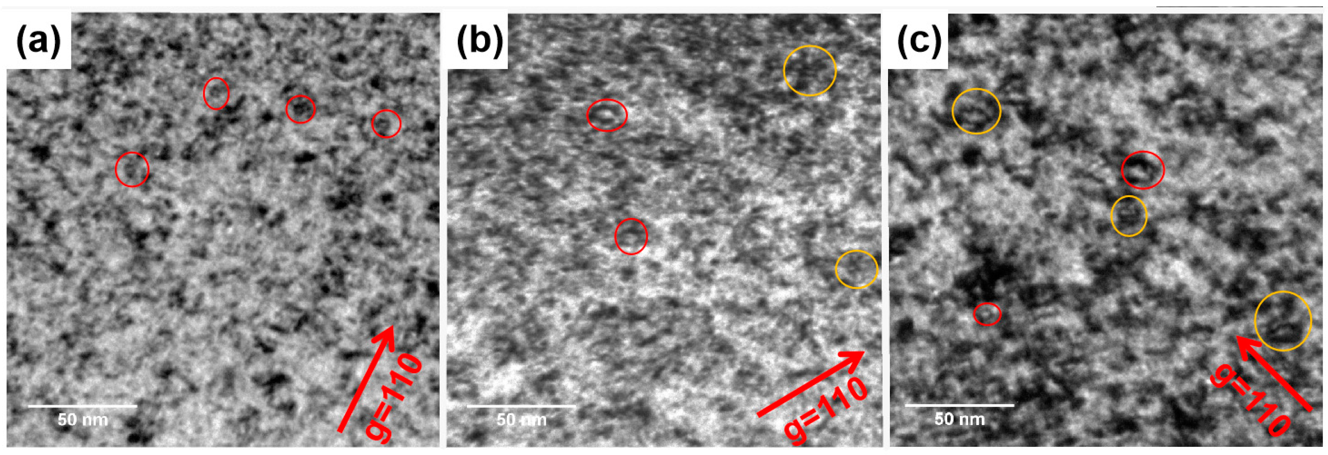
In order to avoid surface effects and a high concentration of self-ion implantation near the damage peak, the analysis was performed in a specific depth range of 400–600 nm (corresponding to damage ranges of 0.5–0.7 dpa, 2.0–2.8 dpa, and 4.0–5.5 dpa). The number of observed dislocation loops varied under different g conditions based on the invisibility criterion of g · b = 0. To exclude the influence of diffraction direction, uniform observation was performed at g = 110. The bright-field image in Figure 3 depicts the “Y + MAX” alloy under various irradiation doses, with a large number of defect clusters visible at all three irradiation doses, including some typical dislocation-loop-like defect structures (shown in red circles in Figure 3). It should be noted that it cannot be ruled out that some of the defect clusters are caused by FIB, which makes it difficult to precisely quantify dislocation loops. However, the TEM image still clearly indicates that the microstructure primarily consisted of visible black dots or small dislocation loops after irradiation at 0.8 dpa (Figure 3a). The size of the dislocation loops and defect clusters increases significantly with the irradiation dose. At 3.5 dpa and 6.1 dpa, large numbers of aggregates formed by the merging of two or more dislocation loops are observed (indicated by yellow circles in Figure 3). Especially at 6.1 dpa, the microstructure is dominated by large-size dislocation loop aggregates and defect clusters. It is worth noting that the visibility of irradiation defects in the TEM image is closely related to the material’s microstructure uniformity. Generally, the contrast of irradiation defects is more apparent in grains with a single lattice orientation, facilitating easy observation. Due to the presence of diffuse nanoparticles and their varied orientations and small sizes in the V-4Cr-4Ti-1.5Y-0.3Ti3SiC2 sample, observing irradiation defects in this material is more challenging. Therefore, irradiation defects are observed inside the larger-size grains.
The bright-field image of V-4Cr-4Ti under the same observation conditions is shown in Figure 4, revealing a growth trend of defect clusters similar to Y + MAX alloys. Different from the Y + MAX alloy, the defect clusters of V-4Cr-4Ti exhibit a higher number density and smaller size, especially at 0.8 dpa and 3.5 dpa. At 6.1 dpa, this difference becomes insignificant.

3.2. Irradiation Hardening

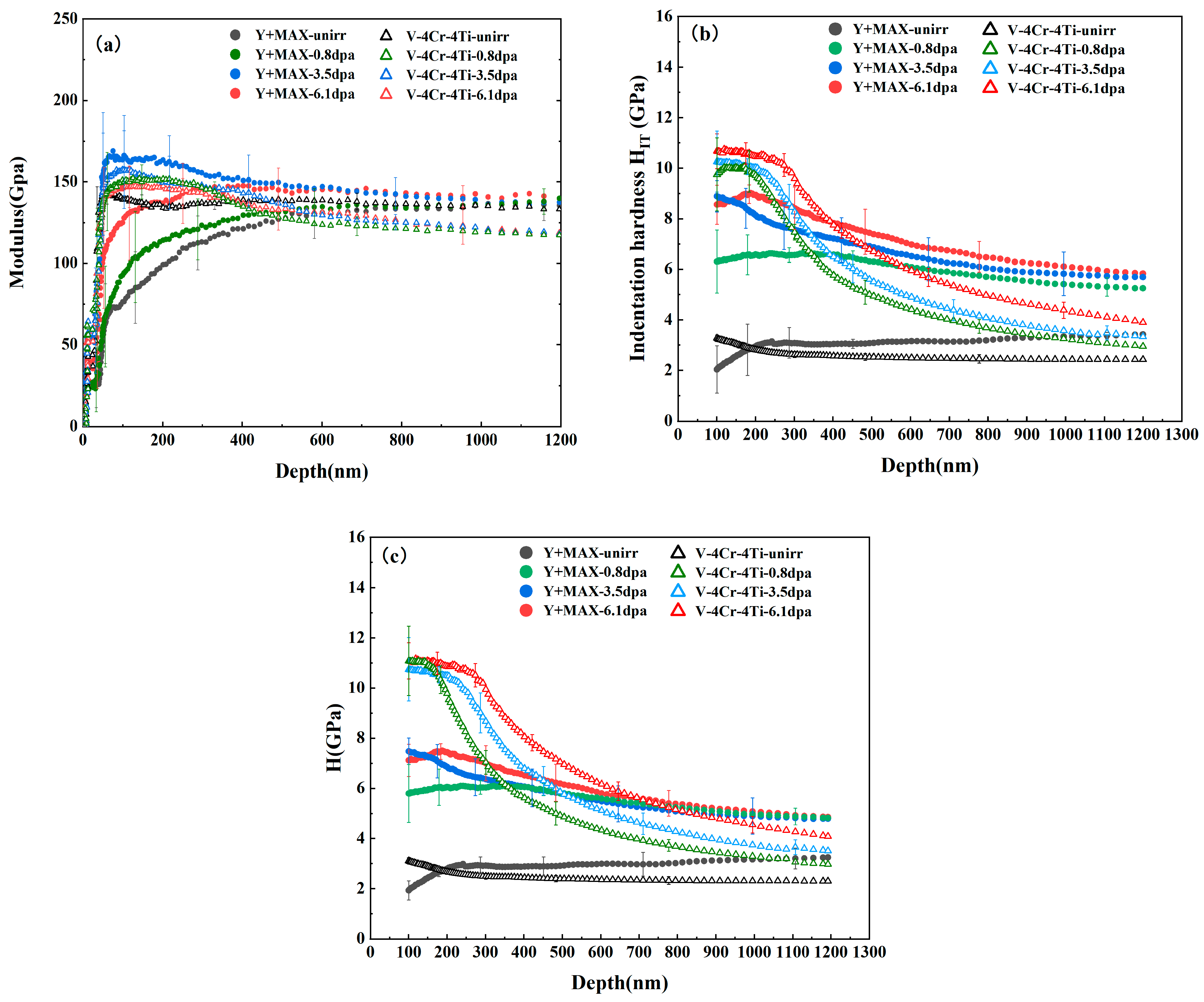
Figure 5a shows the indentation modulus results for V-4Cr-4Ti, and V-4Cr-4Ti-1.5Y-0.3Ti3SiC2 before and after the 2.5 MeV V2+ ion irradiation. As can be seen in the figure, the indentation modulus of irradiated materials exhibits a clear depth dependence. It is widely accepted that the elastic properties are less affected by irradiation damage compared to plastic properties like hardness and yield stress [28]. Therefore, the deep dependence of the indentation modulus is considered to be the effect of irradiation on the pile-up or sink-in behavior during indentation. To minimize the effects of pile-up or sink-in, indentation hardness is corrected using elastic-modulus-based correction (EMC) [28,29], described by
H E M C = H I T × ( E E M C / E ) 2
1 E = ( 1 ν s 2 ) E I T + ( 1 ν I 2 ) E I
1 E E M C = ( 1 ν s 2 ) E s + ( 1 ν I 2 ) E I
where HIT and HEMC are hardness values from nanoindentation testing and EMC modeling, E* and EEMC* are the reduced modulus values, EI and Es are the elastic modulus of the indenter tip and test material, and  ν s  and  ν I  are the Poisson’s ratios of the indenter tip and test material, respectively. EIT is the measured and apparent modulus of the material tested using the Nano Indenter*G200 testing machine. In the nanoindentation tests, EI = 1141 GPa and  ν I  = 0.07 [30] were used for the diamond tip, and Es = 147 GPa and  ν s  = 0.33 were used for Vanadium alloys [31]. Figure 5b portrays the average value of nanoindentation hardness as a function of depth, and Figure 5c shows the hardness values before and after irradiation calculated using the EMC. In comparison, after EMC correction, the hardness of V-4Cr-4Ti increases slightly, while the hardness of V-4Cr-4Ti-1.5Y-0.3Ti3SiC2 decreases slightly.
In the nanoindentation test, the hardness value H is larger when the indenter depth is shallow, and the hardness value gradually decreases with the increase in the indentation depth, which is called the indentation size effect (ISE). Consequently, hardness data within a depth of 100 nm are disregarded due to the indentation size effect [31,32]. The Nix–Gao model is established, as shown in Equation (5), to eliminate the indentation size effect based on the Geometrically Necessary Dislocation (GND) theory [33].
H 2 = H 0 2 ( 1 + h h )
where H0 is the hardness of the material at infinite depth (equivalent to the real hardness of the material), H is the hardness value corresponding to the indentation depth of h, and h* is the characteristic length related to the material and the shape of the indenter. According to Equation (1), the curve shown in Figure 6 is obtained by plotting the square of the nanoindentation hardness (HEMC2) and the reciprocal of the indentation depth (h−1).
As depicted in Figure 6, the irradiated samples exhibit two clear linear relationships. The curve remains relatively flat within the range of 100–173 nm (h−1: 0.0058–0.0100). Above 167 nm (h−1: 0.0010–0.0058), H2 decreases rapidly with the decrease in 1/h, indicating a notable decline in hardness with increasing depth. This behavior can be attributed to the soft substrate effect (SSE), which occurs when the unirradiated area undergoes plastic deformation before the indentation arrives. Thus, the impact of the unirradiated area on hardness measurement must not be disregarded [31]. To mitigate the impact of the soft substrate effect, data within the range of 0.0058–0.0100 nm−1 (100–173nm) are selected for linear fitting of irradiated materials. The fitting result is extrapolated to infinity depth (intersection with the y-axis) to obtain the hardness data. Since there is no soft matrix effect, there is only one linear relationship for the unirradiated samples, and the hardness of the unirradiated samples is extrapolated from this linear relationship in the range of 0–0.0100 nm−1.

4. Discussion

4.1. Effect of Irradiation Dose on Nanoparticles

The average size and number density of nanoparticles in the irradiated samples exhibit a slight decrease compared to those in the non-irradiated area, and the proportion of small-sized nanoparticles increased slightly. However, these changes with the increase in the irradiation dose are not deemed significant. Overall, the nanoparticles in the sample are found to remain stable in the range of irradiation conditions in this work.

4.2. Effect of Irradiation Dose on Defect Clusters

Both materials exhibit the growth of defect clusters with increasing irradiation dose. Such growth is characteristic of the microstructural evolution of metallic materials under ion irradiation [34]. The rapid growth of a dislocation loop occurs via the absorption of mobile clusters and point defects or merging with other dislocation loops [35,36]. This growth in turn leads to a decrease in the number density of dislocation loops. The number density of the dislocation loop in the V-4Cr-4Ti-1.5Y-0.3Ti3SiC2 is shown to be smaller at the same irradiation damage. This difference can be attributed to the boundary between the nanoparticle and the material matrix serving as a trap for adsorbing irradiation defects, such as interstitial atoms, vacancy clusters, and dislocation loops. This was reconfirmed by H. Oka et al. [37], who observed the nucleation process of dislocation loops at the boundary between the nanoparticles and the matrix in ODS steel using in situ transmission electron microscopy. It must be admitted that the accurate and quantitative evaluation of dislocation loops generated by irradiation is hindered by the defects introduced by FIB in this study. In the future, achieving more accurate TEM observation is a critical concern, and the “Flash-polishing” method should be tried to eliminate FIB defects.

4.3. Effect of Irradiation Dose on Hardness

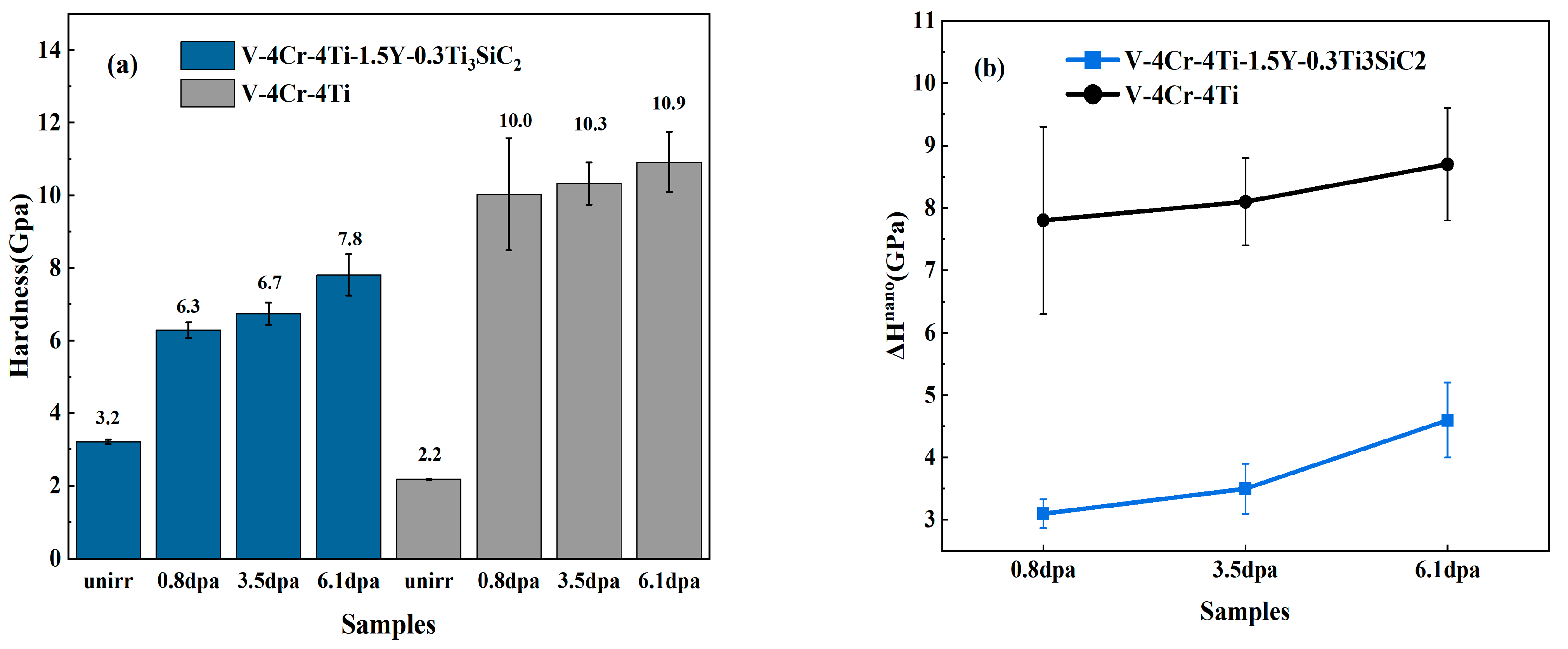
Figure 7a presents a histogram of the hardness obtained using the Nix–Gao model to visually compare the hardnesses of the two materials as a function of irradiation dose. Both materials exhibit significant irradiation hardening, with hardness values increasing as the irradiation damage rises. The V-4Cr-4Ti-1.5Y-0.3Ti3SiC2 alloy demonstrates a larger initial hardness value but a smaller hardness value after irradiation compared to the V-4Cr-4Ti alloy. This higher initial hardening of V-4Cr-4Ti-1.5Y-0.3Ti3SiC2 alloys can be attributed to the dispersion-strengthening effect of nanoparticles, as observed in previous studies [22,23]. Figure 7b shows the trend of hardness increment (∆H = HEMCirr − HEMCunirr) for both samples as a function of dose. The results clearly show that the hardness increment of V-4Cr-4Ti-1.5Y-0.3Ti3SiC2 is significantly lower than that of V-4Cr-4Ti, and the hardness increment of V-4Cr-4Ti does not vary significantly with the dose. Conversely, the hardness increment of V-4Cr-4Ti-1.5Y-0.3Ti3SiC2 exhibits a dose-dependent trend, with a notable increase in hardness from 3.5 dpa to 6.1 dpa. Notably, the hardness value of “V-4Cr-4Ti-0.8 dpa” surpasses that of “Y + MAX-6.1 dpa”. These results suggest that the V-4Cr-4Ti alloy may have already reached a saturation point for irradiation hardening before reaching 0.8 dpa, while V-4Cr-4Ti-1.5Y-0.3Ti3SiC2 may not have reached saturation even at 6.1 dpa. It is evident that V-4Cr-4Ti-1.5Y-0.3Ti3SiC2 exhibits superior resistance to radiation hardening compared to V-4Cr-4Ti. In the study of Luo et al. [19], the initial hardness of V-4Cr-4Ti prepared using the arc melting method was approximately 2.3 GPa, and the hardening value of V-4Cr-4Ti was approximately 9.8 GPa after being irradiated to 35 dpa with Fe2+ ions at 550 °C. The results of their study are comparable to our experimental results, indicating that V-4Cr-4Ti reaches a hardening saturation value of approximately 10 GPa under ion irradiation at around 500 °C.
The source of irradiation hardening lies in the fact that the interstitial atoms and vacancies, dislocation loops, voids, and other defects caused by irradiation are different from the matrix lattice arrangement; this results in the distortion of the crystal lattice and thereby hinders the dislocation motion. The significant increase in sink strength due to the dispersed nanoparticles suppresses the concentration of interstitial atoms and vacancies, thereby suppressing the formation and growth rate of irradiation defects [27,38]. At the same time, the boundary between the nanoparticles and the matrix during irradiation also captures irradiation defects [37,39], further suppressing irradiation hardening.

5. Conclusions

The irradiation hardening and microstructure of V-4Cr-4Ti-1.5Y-0.3Ti3SiC2 and V-4Cr-4Ti alloys were investigated after irradiation with 2.5 MeV V2+ ions at 500 °C with varying doses. The key findings are as follows:
(1)
After irradiation, defect clusters are present in both materials. The growth and merging of defect clusters with irradiation dose are observed in both materials.
(2)
Both materials exhibit significant irradiation hardening, and hardness increases as the irradiation dose rises. V-4Cr-4Ti reaches hardening saturation before 0.8 dpa, whereas V-4Cr-4Ti-1.5Y-0.3Ti3SiC2 may not saturate even at 6.1 dpa.
(3)
Compared with V-4Cr-4Ti, V-4Cr-4Ti-1.5Y-0.3Ti3SiC2 had a larger initial hardening value and smaller irradiation hardening value. This can be attributed to the fact that the boundary between the nanoparticles and the matrix significantly increases the sink strength, suppressing defect evolution and irradiation hardening.

Author Contributions

Conceptualization, Y.W. and P.Z. (Pengfei Zheng); methodology, Y.Z., H.L. and W.Q.; validation, Y.W. and P.Z. (Pengfei Zheng); investigation, Y.Z., H.L., W.Q., G.Z., F.L. and M.Z.; resource, G.Z., F.L. and M.Z.; analysis, Y.Z., W.Q., G.Z., F.L. and M.Z.; supervision, P.Z. (Pengfei Zheng); resources, Y.W. and P.Z. (Pengbo Zhang); data curation, Y.Z. and H.L.; writing—original draft preparation, Y.Z.; writing—review and editing, Y.W. and P.Z. (Pengfei Zheng); project administration, Y.W. and P.Z. (Pengfei Zheng); funding acquisition, Y.W., P.Z. (Pengfei Zheng) and P.Z. (Pengbo Zhang). All authors have read and agreed to the published version of the manuscript.

Funding

This work was supported by the National Natural Science Foundation of China (No. 12275073 and No. 12175028) and the Innovation Program of Southwestern Institute of Physics (No. 202301XWCX004-02).

Data Availability Statement

Data presented in this article are available on request from the corresponding author.

Acknowledgments

We acknowledge the assistance in TEM sample preparation and irradiation experiments from the School of Physics and Technology of Wuhan University and thank the Analysis and Testing Center of Wuhan University for supporting TEM.

Conflicts of Interest

The authors declare no conflicts of interest.

References

  1. Muroga, T.; Chen, J.M.; Chernov, V.M.; Kurtz, R.J.; Le Flem, M. Present status of vanadium alloys for fusion applications. J. Nucl. Mater. 2014, 455, 263–268. [Google Scholar] [CrossRef]
  2. Luo, L.-M.; Zhao, Z.-H.; Yao, G.; Wu, Y.-C. Recent progress on preparation routes and performance evaluation of ODS/CDS-W alloys for plasma facing materials in fusion devices. J. Nucl. Mater. 2021, 548, 152857. [Google Scholar] [CrossRef]
  3. Doñate Buendia, C.; Kürnsteiner, P.; Stern, F.; Wilms, M.B.; Streubel, R.; Kusoglu, I.M.; Tenkamp, J.; Bruder, E.; Pirch, N.; Barcikowski, S.; et al. Microstructure formation and mechanical properties of ODS steels built by Laser Additive Manufacturing of nanoparticle coated iron-chromium powders. Acta Mater. 2020, 206, 116566. [Google Scholar] [CrossRef]
  4. Shibayama, T.; Yamagata, I.; Kurishita, H.; Kayano, H. Development of oxide dispersion strengthened vanadium alloy and its properties. J. Nucl. Mater 1996, 239, 162–169. [Google Scholar] [CrossRef]
  5. Yasuda, H.; Mori, H. Effect of fast neutron irradiation on the microstructure in particle dispersed ultra-fine grained VY alloys. J. Nucl. Mater. 2004, 45, 29–33. [Google Scholar]
  6. Kobayashi, S.; Tsuruoka, Y.; Nakai, K.; Kurishita, H. Effect of neutron irradiation on the microstructure and hardness in particle dispersed ultra-fine grained V–Y alloys. J. Nucl. Mater. 2004, 329, 447–451. [Google Scholar] [CrossRef]
  7. Nagasaka, T.; Murogaa, T.; Li, M.M. Tensile property of low activation vanadium alloy after liquid lithium exposure. Fusion Eng. Des. 2006, 81, 307–313. [Google Scholar] [CrossRef]
  8. Li, M.M.; Nagasaka, T. Biaxial thermal creep of two heats of V-4Cr-4Ti at 700 and 800 °C in a liquid lithium environment. J. Nucl. Mater. 2007, 367, 788–793. [Google Scholar] [CrossRef]
  9. Li, M.M.; Hoelzer, D.T.; Grossbeck, M.L. The Influence of lithium environment on tensile behavior and microstructure of V–4Cr–4Ti. J. Nucl. Mater. 2009, 392, 364–370. [Google Scholar] [CrossRef]
  10. Furuno, T.; Kurishita, H.; Nagasaka, T.; Nishimura, A.; Muroga, T.; Sakamoto, T.; Kobayashi, S.; Nakai, K.; Matsuo, S.; Arakawa, H. Effects of grain size on high temperature creep of fine grained, solution and dispersion hardened V–1.6Y–8W–0.8TiC. J. Nucl. Mater. 2011, 417, 299–302. [Google Scholar] [CrossRef]
  11. Sakamoto, T.; Kurishita, H.; Furuno, T.; Nagasaka, T.; Kobayashi, S.; Nakai, K.; Matsuo, S.; Arakawa, H.; Nishimura, A.; Muroga, T. Uniaxial creep behavior of nanostructured.; solution and dispersion hardened V–1.4Y–7W–9Mo–0.7TiC with different grain sizes. Mater. Sci. Eng. A 2011, 528, 7843–7850. [Google Scholar] [CrossRef]
  12. Tallman, D.J.; Anasori, B.; Barsoum, M.W. A critical review of the oxidation of Ti2AlC,Ti3AlC2 and Cr2AlC in air. Mater. Res. Lett. 2013, 1, 115–125. [Google Scholar] [CrossRef]
  13. Sun, Z. Progress in research and development on MAX phases: A family of layered ternary compounds. Int. Mater. Rev. 2011, 56, 143–166. [Google Scholar] [CrossRef]
  14. Huang, Q.; Liu, R.; Lei, G.; Huang, H.; Li, J.; He, S.; Li, D.; Yan, L.; Zhou, J. Irradiation resistance of MAX phases Ti3SiC2 and Ti3AlC2: Characterization and comparison. J. Nucl. Mater. 2015, 465, 640–647. [Google Scholar] [CrossRef]
  15. Le Flem, M.; Liu, X.; Doriot, S.; Cozzika, T.; Monnet, I. Irradiation damage in Ti3(Si,Al)C2: A TEM investigation. Int. J. Appl. Ceram. Technol. 2010, 7, 766–775. [Google Scholar] [CrossRef]
  16. Wang, C.; Yang, T.; Kong, S.; Xiao, J.; Xue, J.; Wang, Q.; Hu, C.; Huang, Q.; Wang, Y. Effects of He irradiation on Ti3AlC2: Damage evolution and behavior of He bubbles. J. Nucl. Mater. 2013, 440, 606–611. [Google Scholar] [CrossRef]
  17. Watanabe, H.; Yamasaki, K.; Higashijima, A.; Taguma, H.; Nagasaka, T.; Muroga, T. Microstructural changes of Y-doped V-4Cr-4Ti alloys after ion and neutron irradiation. Nucl. Mater. Energy 2016, 9, 447–450. [Google Scholar] [CrossRef]
  18. Zhang, Y.F.; Li, R.R.; Diao, S.Z.; Wan, F.R.; Zhan, Q. Plasticity Improvement and Radiation Hardening Reduction of Y Doped V-4Cr-4Ti Alloy. J. Nucl. Mater. 2022, 560, 153508. [Google Scholar] [CrossRef]
  19. Luo, H.; Luo, F.; Chen, Y.; Wang, J.; Liu, Q.; Li, F.; Xie, Z.; Lin, W.; Guo, L. Effect of yttrium content on microstructure and irradiation behavior of V-4Cr-4Ti-xY alloys. J. Nucl. Mater. 2022, 559, 153480. [Google Scholar] [CrossRef]
  20. Zhang, Y.F.; Sun, X.Y.; Ma, B.; Wang, J.; Luo, L.; Wu, Y.C. Investigation of the Y effect on the microstructure response and radiation hardening of PM V-4Cr-4Ti alloys after irradiation with D ions. Metals 2023, 13, 541. [Google Scholar] [CrossRef]
  21. Watanabe, H.; Muroga, T.; Nagasak, T. Effects of Irradiation Environment on V–4Cr–4Ti Alloys. Plasma Fusion Res. 2017, 12, 2405011. [Google Scholar] [CrossRef]
  22. Zheng, P.F.; Chen, J.M.; Nagasaka, T.; Muroga, T.; Zhao, J.J.; Xu, Z.Y.; Li, C.H.; Fu, H.Y.; Chen, H.; Duan, X.R. Effects of dispersion particle agents on the hardening of V–4Cr–4Ti alloys. J. Nucl. Mater. 2014, 455, 669–675. [Google Scholar] [CrossRef]
  23. Zhang, Y.F.; Du, J.K.; Liu, P.P.; Zheng, P.F.; Yang, S.W.; Wan, F.R.; Zhan, Q. Response of microstructure and hardening to deuterium ion irradiation in V-4Cr-4Ti-1.8Y-0.4Ti3SiC2 and V-4Cr-4Ti alloy. Fusion Eng. Des. 2020, 159, 111789. [Google Scholar] [CrossRef]
  24. Chen, Y.; Guo, L.; Long, Y.; Xie, Z.; Luo, H.; Lin, W.; Huang, Q. Establishment of multi-beam irradiation facility at Wuhan University. Nucl. Inst. Methods Phys. Res. A 2022, 1040, 167202. [Google Scholar] [CrossRef]
  25. Mansur, L.K. Theory of transitions in dose dependence of radiation effects in structural alloys. J. Nucl. Mater. 1993, 206, 306–323. [Google Scholar] [CrossRef]
  26. Kartamyshev, A.I.; Lipnitskii, A.G.; Boev, A.O.; Nelasov, I.V.; Maksimenko, V.N.; Aksyonov, D.A.; Nguyen, T.K. Angular dependent interatomic potential for Ti-V system for molecular dynamics simulations. Model. Simul. Mater. Sci. Eng. 2020, 28, 055010. [Google Scholar] [CrossRef]
  27. Zinkle, S.J.; Snead, L.L. Designing Radiation Resistance in Materials for Fusion Energy. Annu. Rev. Mater. Res. 2014, 44, 241–267. [Google Scholar] [CrossRef]
  28. Liu, Y.; Kondo, S.; Yu, H.; Yabuuchi, K.; Kasada, R. Evaluation of irradiation hardening in ODS-Cu and non ODS-Cu by nanoindentation hardness test and micro-pillar compression test after self-ion irradiation. Nucl. Mater. Energy 2021, 26, 100903. [Google Scholar] [CrossRef]
  29. Hasenhuetl, E.; Kasada, R.; Zhang, Z.; Yabuuchi, K.; Huang, Y.-J.; Kimura, A. Evaluation of Ion-Irradiation Hardening of Tungsten Single Crystals by Nanoindentation Technique Considering Material Pile-Up Effect. Mater. Trans. 2017, 58, 749–756. [Google Scholar] [CrossRef]
  30. Fischer-Cripps, A.C. Critical review of analysis and interpretation of nanoindentation test data. Surf. Coat. Technol. 2006, 200, 4153–4165. [Google Scholar] [CrossRef]
  31. Miyazawa, T.; Nagasaka, T.; Kasada, R.; Hishinuma, Y.; Muroga, T.; Watanabe, H.; Yamamoto, T.; Nogami, S.; Hatakeyama, M. Evaluation of Irradiation Hardening of Ion-Irradiated V-4Cr-4Ti and V-4Cr-4Ti-0.15Y Alloys by Nanoindentation Techniques. J. Nucl. Mater. 2014, 455, 440–444. [Google Scholar] [CrossRef]
  32. Yan, H.; Zhan, Z.; Wang, J.; Okonkwo, B.O.; Han, E.-H. Effects of MeV Fe Ions Irradiation on the Microstructure and Property of Nuclear Grade 304 Stainless Steel: Characterized by Positron Annihilation Spectroscopy, Transmission Electron Microscope and Nanoindentation. Acta Metall. Sin. Engl. Lett. 2021, 34, 1695–1703. [Google Scholar] [CrossRef]
  33. Nix, W.D.; Gao, H. Indentation size effects in crystalline materials: A law for strain gradient plasticity. J. Mech. Phys. Solids 1998, 46, 411–425. [Google Scholar] [CrossRef]
  34. Muroga, T.; Miyazawa, T.; Nagasaka, T.; Atanabe, H.W. Correlation of Microstructural Evolution in V-4Cr-4Ti by Heavy Ion and Neutron Irradiations. Plasma Fusion Res. 2016, 11, 2405007. [Google Scholar] [CrossRef]
  35. Li, Y.; Wang, L.; Ran, G.; Yuan, Y.; Wu, L.; Liu, X.; Qiu, X.; Sun, Z.; Ding, Y.; Han, Q.; et al. In-situ TEM investigation of 30 keV he+ irradiated tungsten: Effects of temperature, fluence, and sample thickness on dislocation loop evolution. Acta Mater. 2021, 206, 116618. [Google Scholar] [CrossRef]
  36. Yipeng, L.; Miaosen, Y.; Guang, R.; Ning, G.; Yang, C.; Qing, H.; Hui, W.; Zhehui, Z.; Jinchi, H. In-situ TEM study and molecular dynamics simulation of dislocation loop evolution in FeCrAl alloysunder Fe+ irradiation. Mater. Today Energy 2021, 21, 100788. [Google Scholar]
  37. Oka, H.; Watanabe, M.; Kinoshita, H.; Shibayama, T.; Hashimoto, N.; Ohnuki, S.; Yamashita, S.; Ohtsuka, S. In situ observation of damage structure in ODS austenitic steel during electron irradiation. J. Nucl. Mater. 2011, 417, 279–282. [Google Scholar] [CrossRef]
  38. Srinivasan, S.; Kale, C.; Hornbuckle, B.C.; Darling, K.A.; Chancey, M.R.; Hernandez-Rivera, E.; Chen, Y.; Koenig, T.R.; Wang, Y.Q.; Thompson, G.B.; et al. Radiation tolerance and microstructural changes of nanocrystalline Cu-Ta alloy to high dose self-ion irradiation. Acta Mater. 2020, 195, 621–630. [Google Scholar] [CrossRef]
  39. Xuxiao, H.; Chonghong, Z.; Mengke, N.; Zhaonan, D.; Jinsung, J.; Tieshan, W.; Akihiko, K. A comparison study of change in hardness and microstructures of a Zr-added FeCrAl ODS steel irradiated with heavy ions. Mater. Sci. Eng. A 2022, 841, 143050. [Google Scholar]
Figure 1. (a) SRIM calculation of damage under 2.5 MeV V2+ irradiation. (b) The neutron irradiation temperature corresponding to the ion irradiation temperature of 773 K as a function of the ratio of dose rates.
Metals 14 00141 g001
Figure 2. (a1,b1,c1,d1) TEM micrographs of the unirradiated region, Y + MAX-0.8 dpa, Y + MAX-3.5 dpa, and Y + MAX-6.1 dpa, respectively; (a2,b2,c2,d2) corresponding nanoparticle size distributions.
Metals 14 00141 g002
Figure 3. TEM bright-field image of V-4Cr-4Ti-1.5Y-0.3Ti3SiC2 alloys (red circles are typical dislocation loops, yellow circles are merged dislocation loops): (a) Y + MAX-0.8 dpa, (b) Y + MAX-3.5 dpa, (c) Y + MAX-6.1 dpa.
Metals 14 00141 g003
Figure 4. TEM bright-field image of V-4Cr-4Ti alloys (red circles are typical dislocation loops, yellow circles are merged dislocation loops): (a) V-4Cr-4Ti-0.8 dpa, (b) V-4Cr-4Ti-3.5 dpa, (c) V-4Cr-4Ti-6.1 dpa.
Metals 14 00141 g004
Figure 5. (a) Indentation modulus EIT before and after ion irradiation. (b) Indentation hardness HIT as a function of indentation depth. (c) Modulus-corrected indentation hardness HEMC as a function of indentation depth.
Metals 14 00141 g005
Figure 6. The square of the hardness value (H2) obtained using the Nix–Gao model as a function of the indentation depth (1/h).
Metals 14 00141 g006
Figure 7. (a) Hardness of V-4Cr-4Ti-1.5Y-0.3Ti3SiC2 and V-4Cr-4Ti before and after irradiation. (b) Trend of hardness increment with dose.
Metals 14 00141 g007
Table 1. Experimental conditions.
SampleMaterialIrradiation Fluence
(ions cm−2)
Peak Damage
(dpa)
Y + MAX-unirrV-4Cr-4Ti-1.5Y-0.3Ti3SiC2unirradiated-
Y + MAX-0.8 dpaV-4Cr-4Ti-1.5Y-0.3Ti3SiC21 × 10150.8
Y + MAX-3.5 dpaV-4Cr-4Ti-1.5Y-0.3Ti3SiC24 × 10153.5
Y + MAX-6.1 dpaV-4Cr-4Ti-1.5Y-0.3Ti3SiC27 × 10156.1
V-4Cr-4Ti-unirrV-4Cr-4Tiunirradiated-
V-4Cr-4Ti-0.8 dpaV-4Cr-4Ti1 × 10150.8
V-4Cr-4Ti-3.5 dpaV-4Cr-4Ti4 × 10153.5
V-4Cr-4Ti-6.1 dpaV-4Cr-4Ti7 × 10156.1
Disclaimer/Publisher’s Note: The statements, opinions and data contained in all publications are solely those of the individual author(s) and contributor(s) and not of MDPI and/or the editor(s). MDPI and/or the editor(s) disclaim responsibility for any injury to people or property resulting from any ideas, methods, instructions or products referred to in the content.