1. Introduction
Fossil fuels, including oil, coal, and natural gas, are major contributors to the increasing concentration of greenhouse gases, particularly carbon dioxide, in the atmosphere. The resulting emissions lead to global warming, causing various adverse effects such as the melting of icebergs, increases in sea levels, and other related phenomena that significantly impact Earth’s ecosystems. Limiting greenhouse gas concentrations is widely recognized as a crucial step in mitigating the most devastating effects of climate change. While it is challenging to halt global temperature rise completely, efforts to reduce greenhouse gas emissions are essential to minimizing the severity of climate-related impacts. Solar power generation, particularly via photovoltaic (PV) technology, is considered one of the most promising alternatives to fossil fuels. The solar industry aims to provide competitive power generation products that can effectively replace fossil fuels and other renewable energy sources. By harnessing the energy from the sun, solar power offers a clean and renewable source of electricity that can help reduce greenhouse gas emissions and combat climate change. As the PV industry continues to evolve and advance, increased adoption of solar power generation is expected. This transition to renewable energy sources like solar power is crucial for a sustainable and environmentally friendly future.
According to the latest International Technology Roadmap for Photovoltaic, it is predicted that the global production capacity of crystalline silicon (c-Si) cells and photovoltaic modules will increase to 600 GWp by the end of 2022 (14th edition, 2023) [
1]. One of the factors contributing to the growth in the production capacity of c-Si cells and photovoltaic modules is the advancement in passivated rear emitter cell (PERC) technology. PERC technology has played a significant role in improving the average module efficiencies of crystalline silicon solar cells. Using larger wafers has also enabled the development of new module power classes, including those with a power rating of 600 W and above. In terms of technological development, the construction of new cell and module capacities in 2022 shifted from PERC to n-type-based tunneling oxide passivated contacts (TOPCon) and silicon heterojunction (SHJ) technologies [
1]. SHJ solar cells are known for their high open-circuit voltage, conversion efficiency, excellent bifacial factors, and facilitation of low-temperature processes. These attributes make SHJ solar cells a potentially cost-competitive option for large-scale industrialization [
1,
2,
3]. Many organizations have investigated heterojunction technology in relation to crystalline solar cells, which constitute a promising candidate for further increasing solar cell efficiency.
The typical structure of a crystalline Si heterojunction solar cell includes silicon wafers, hydrogenated amorphous silicon (a-Si H) films, transparent conductive oxide (TCO) films, and metal grids. Indium–tin–oxide is a commonly used TCO in solar cell and display applications that serves as an electrical contact. On the other hand, the metal grid, usually made of silver (Ag) paste, is applied to the front side of the silicon heterojunction to facilitate electrical conduction. Metallization pastes containing silver are critical yet costly non-silicon materials used in current c-Si solar cell technologies. It is essential to continue all efforts to lower silver consumption to achieve further cost reductions as silver is currently cost-critical due to global market dependency. On top of a continuous decrease in silver consumption at the cell-manufacturing level, silver’s replacement is still considered, with copper (Cu) being the envisioned substitute [
1]. Copper is mainly used in applications related to interconnects in semiconductor devices due to its high electrical conductivity, resistance to electromigration, and thermal conductivity. Recently, Cu electroplating metallization has attracted much attention with respect to SHJ solar cell processing because it provides excellent gap-filling behavior and facilitates the miniaturization of deposited components. It also offers the advantages of a high deposition rate, the use of simple equipment, and low deposition temperatures [
4,
5,
6,
7].
In the copper metallization process applied to silicon heterojunction (SHJ) solar cells, one of the primary challenges is achieving selective plating on the transparent conductive oxide film and ensuring proper adhesion between the plated finger and the metal oxide layer. Traditionally, the plating process for SHJ solar cells involves a sequence where full-area seed layers are deposited after the preparation of the SHJ substrate, photolithography, and copper electroplating [
5]. These seed layers are typically applied using physical vapor deposition (PVD) or sputtering techniques. The purpose of the metal seed layer is to enhance lateral conductivity and improve the adhesion between the plated electrode and the TCO film. By depositing a seed layer made of a metal such as copper, the lateral conductivity of the electrode can be improved, ensuring efficient current flow across the cell. Additionally, the seed layer promotes better adhesion between the plated copper electrode and the TCO film, thereby minimizing the risk of detachment or delamination.
Electroplated copper films exhibit a distinctive characteristic known as self-annealing, which involves grain growth at room temperature [
8,
9,
10,
11,
12,
13]. After the electroplating process, the grain size of the copper film can increase to several micrometers during self-annealing. This phenomenon is accompanied by changes in resistivity, internal stress, microstructure, texture, and impurity distribution [
14,
15,
16,
17]. The mechanism behind self-annealing in electroplated copper films is not fully understood, but several proposed explanations exist. C.R. Lee et al. suggested that a reduction in grain boundary energy and the release of elastic energy from dislocations could be the driving forces behind self-annealing [
14]. According to this hypothesis, the rearrangement of grains and dislocations lead to the growth of larger grains, thereby reducing defects and strain energy. Another idea proposed by C.H. Lee et al. suggests that the presence of additives in the plating bath, or electrolyte, plays a crucial role in self-annealing. These additives adsorb onto the electroplated film, creating a high density of impurities, dislocations, and residual stresses, which leads to the formation of fine particles [
15]. The exact interactions between the additives and the copper film and their influence on self-annealing are still not fully understood.
The issue of poor adhesion between copper and the transparent conductive oxide layer has been identified in relation to direct copper electroplating on TCO surfaces. This problem can lead to the detachment of the copper layer from the TCO, posing challenges for the use and development of reliable copper metallization techniques. Research by P.H. Chen et al. highlighted the weak adhesion between copper and aluminum-doped zinc oxide (AZO). The peel force measurements for electroplated copper on a copper seed layer on AZO were reported to be 0.39 N/mm for the maximum value and 0.20 N/mm for the average peel force, indicating poor adhesion between copper and AZO [
18].
To address this issue, several studies have investigated methods for improving the adhesion of metal layers to different TCO materials. For instance, S.H. Lee researched copper-plated silicon heterojunction solar cells, focusing on using a Cu-X alloy seed layer on indium tin oxide [
19]. They deposited 500 nm of Cu-X alloy seed layers by co-depositing copper with additives such as manganese (Mn), nickel (Ni), and aluminum (Al) using an evaporator. The results showed that the contacts with the pure copper, Cu-Al alloy, and Cu-Mn alloy seed layers were prone to detachment from the ITO surface during tape tests. However, the connection with the Cu-Ni alloy seed layer exhibited stronger adhesion, as the connection remained intact after the tape test. Furthermore, tape tests conducted on SHJ solar cells with Cu-X/Cu/Ag busbars using different Cu-X seed layers confirmed that the Cu-Ni seed layer demonstrated better adhesion than Cu, Cu-Mn, and Cu-Al [
19]. These studies emphasize the importance of improving the adhesion between copper and TCO layers to enhance the reliability and performance of copper metallization techniques for solar cell applications. Further research is needed to explore and develop effective methods for achieving robust and durable adhesion between copper and various TCO materials.
In recent research conducted by Politze et al., the authors investigated using Fe electroplating as an initial layer for subsequent Ni and Cu plating on polished or pyramidally textured indium–tin–oxide-coated silicon substrates [
20]. The Fe layer acted as an intermediate between the ITO-coated substrate and the Cu layer. Cu layers of up to 15 μm were deposited on the Ni/Fe intermediate layer. The pull-off stresses, which indicate adhesion strength, of the Cu/Ni/Fe/ITO/Si stack were measured to be 1.44 MPa for the polished substrates and 1.28 MPa for the pyramidally textured substrates [
20]. Interestingly, Politze et al. also examined the direct electroplating of Cu onto the Fe layer without the Ni layer. In this case, the metal stack (Cu/Fe/ITO/Si) exhibited poor adhesion and lifted from the substrate. However, when a thin, conformal Ni layer was deposited between the Fe and Cu layers, the Fe/Ni/Cu layer stack maintained good adhesion, even with a Cu layer thickness of 15 μm [
20]. This suggests that the Ni layer promotes adhesion between the Cu and Fe layers. Based on the results of their experiments, it is evident that the direct electroplating of Cu on the Fe layer does not result in adherent metal stacks. However, including a thin Ni layer between Fe and Cu improves adhesion properties, allowing for a more stable metal stack to form. In the current study, the authors deposited electroplated Cu films on a sputtered pure copper seed layer, demonstrating good adhesion. The microstructure and mechanical properties of the electroplated Cu films were systematically studied to evaluate their likely suitability for use in heterojunction technology for crystalline solar cells.
3. Results and Discussion
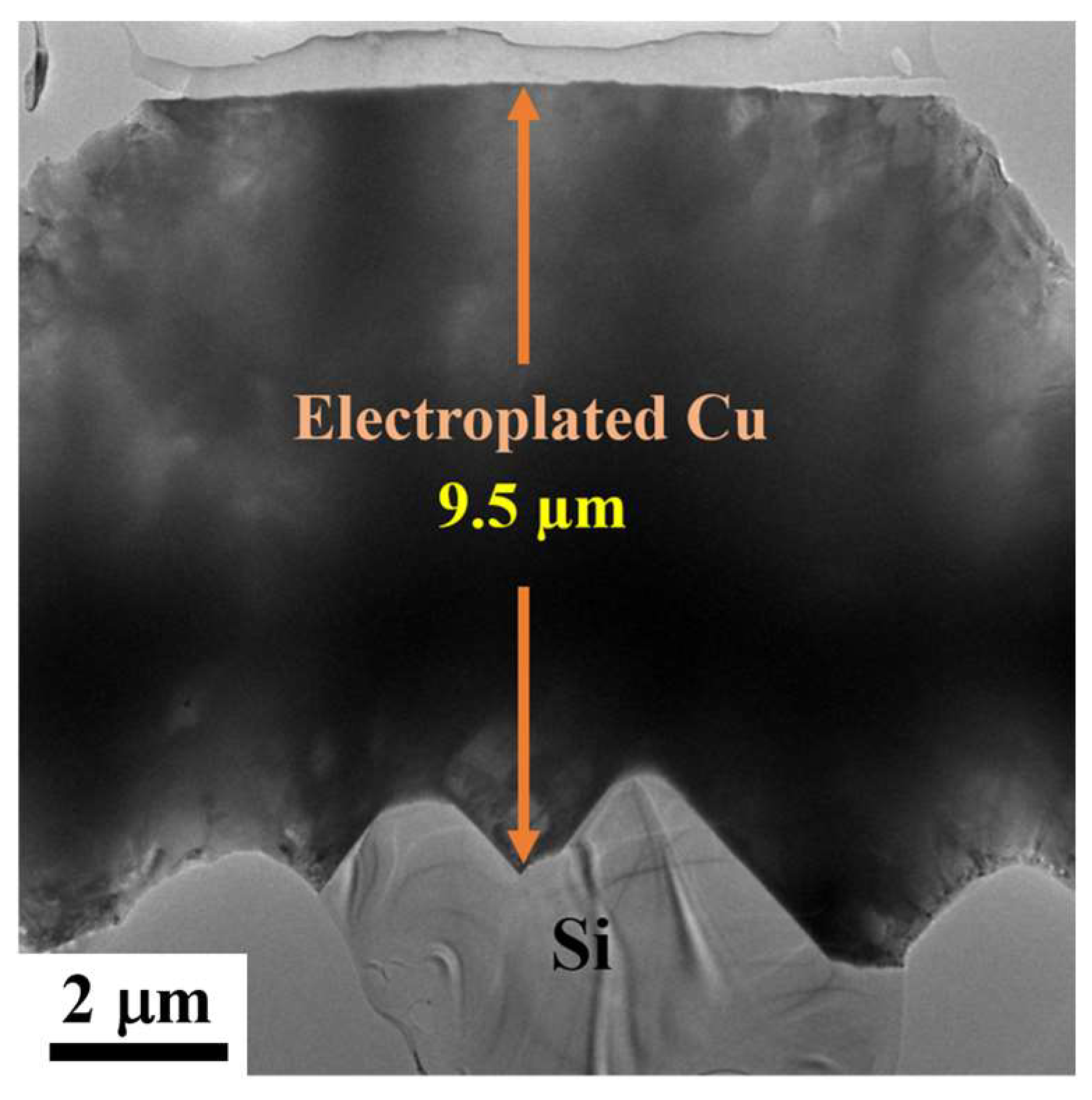
The typical TEM cross-sectional views of the copper electroplated on Cu(S)/ITO/Si are shown in
Figure 1. The thickness of the electroplated copper film is about 9.5 µm, as demonstrated in
Figure 1. The electroplated copper is very dense, and it was deposited conformally on a textured structure. The TEM morphologies of the as-deposited and annealed samples are shown in
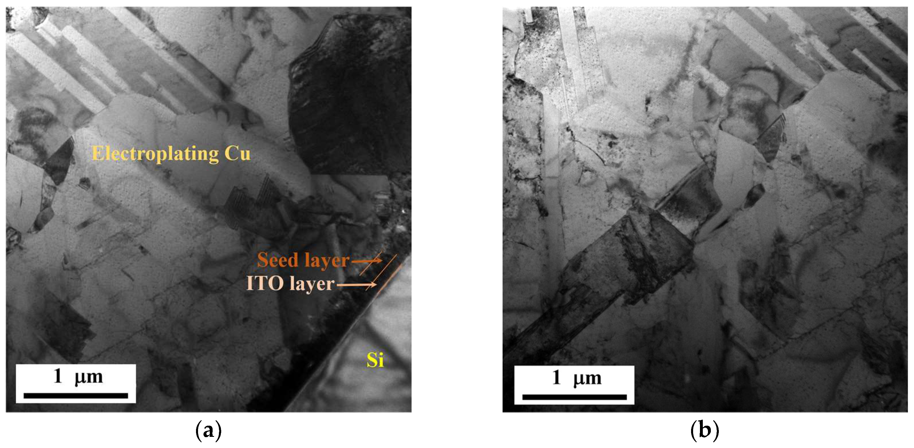
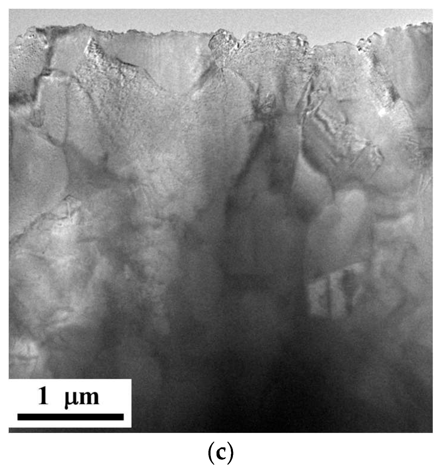
Figure 2 and
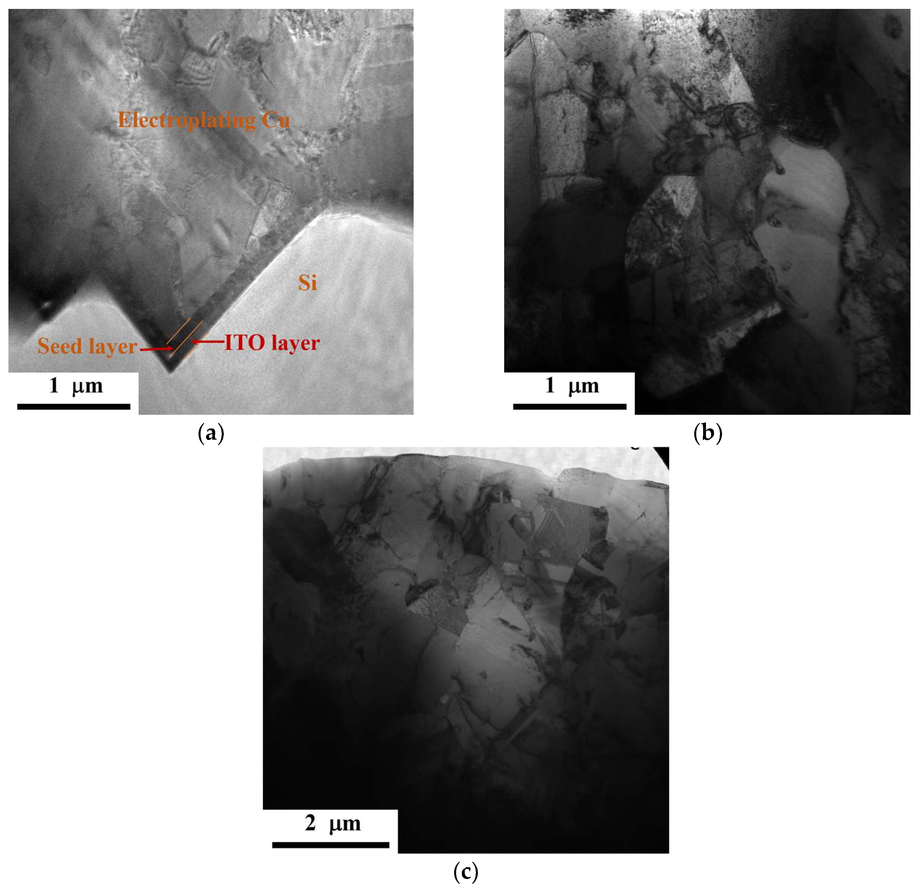
Figure 3.
Figure 2a–c present TEM images of the as-deposited sample, focusing on the bottom, middle, and top parts, respectively. The sputtered ITO film has a thickness of about 100 nm, while the copper film is approximately 140 nm thick. The continuous copper seed layer remained intact during the copper-electroplating process, showing no severe corrosion in the copper sulfate solution. However, it is possible that the copper electrolyte reached the ITO surface due to partial erosion of the copper seed layer, leading to the emergence of voids or gaps at the copper–ITO interface. The electroplated copper film exhibits a twin structure, and its grain size is around 1 µm. The interface between the electroplated copper and the seed layer appears compact, presenting no micro-voids. This indicates good adhesion between the seed layer and the ITO film.
The TEM images of the bottom, middle, and top parts of the annealed sample are shown in
Figure 3a–c, respectively. The thicknesses of the sputtered ITO and copper films on the Cu(s)/ITO/Si samples are approximately the same, i.e., around 100 nm. The copper seed layer also remains continuous. Like the as-deposited sample, the annealed sample exhibits twin structures in the electroplated copper layer, with a grain size of approximately 1 µm. The TEM morphologies of the as-deposited and annealed samples appear almost identical, suggesting that the annealing treatment did not significantly alter the average grain size. In the as-deposited sample, grain growth occurred through the coalescence of small grains during self-annealing. The growth continued until complete recrystallization into large, twinned grains occurred [
9]. Lee et al. prepared a nanocrystalline ultrahigh-strength Cu film produced using the direct current electrodeposition method and investigated the relationship between the microstructure and the electrical/mechanical properties during self-annealing [
14]. The microstructure of the as-deposited film consisted of ultrafine grains with different orientations with respect to the neighboring grains. As the time after deposition increased, the fraction of recrystallized grains increased due to the self-annealing effect. The recrystallized grains often contained twins and stacking faults with a low dislocation density. The combined effect of the reduction in grain boundary energy and the elastic energy of dislocations could have led to the observed self-annealing in the investigated Cu film. The average grain size was about 900 nm for the electroplated Cu films 672 h after deposition [
20].
Residual stress, interfacial reactions, film thickness, and film microstructure influence materials system’s adhesion behavior [
21,
22,
23,
24]. Usually, these factors are often interconnected and challenging to decouple. Electron microscopy can be used to investigate interfacial reactions, film thickness, and film microstructure. Residual stress, which can develop during the growth of thin films, is a critical concern in many technological applications. Excessive residual stress levels can significantly impact material components and devices’ performance, reliability, and durability. High tensile stress can lead to film cracking or delamination in extreme cases. Residual stress distributions can significantly impact thin films’ adhesion and fracture toughness. Residual stress is an essential issue in thin film applications since it can limit the range of performance. Measuring residual stress (or strain) is critical for understanding thin films’ behavior. Wafer curvature techniques are commonly used during deposition to measure residual stress. Other methods, such as X-ray diffraction (XRD), holographic transmission electron microscopy (TEM), micro-Raman spectroscopy, and backscattered electron diffraction, have also been used for residual stress measurement [
25]. Among the various methods used for strain determination, X-ray diffraction (XRD) techniques are commonly used for strain determination applied to thin films and materials. XRD-based techniques provide valuable information about phases, crystallographic orientation, the presence of other crystallographic features, and material composition. These details are crucial for interpreting stress and strain data accurately. By analyzing the diffraction patterns obtained from XRD measurements, researchers can determine the strain present in the analyzed material. The diffraction peaks observed in the pattern correspond to specific crystallographic planes of a material’s crystal structure. The positions and intensities of these peaks can be analyzed to extract information about the lattice spacing and crystal strain. X-ray techniques allow researchers to quantify the strain in thin films and understand such strain’s distribution across the material. This information is essential for evaluating the mechanical properties, performance, and reliability of thin film coatings or devices.
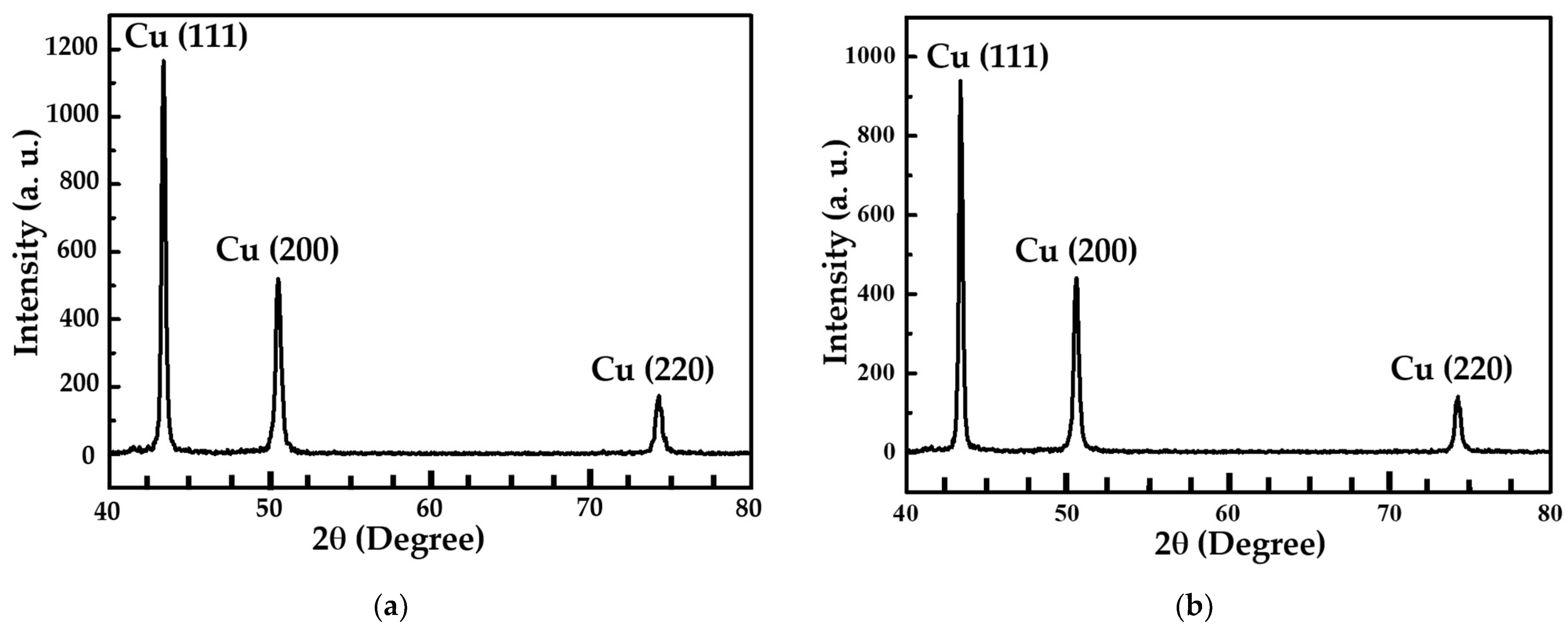
In the XRD analyses conducted for the as-deposited sample and samples annealed at 200 °C for 30 min (
Figure 4a,b), the diffraction pattern reveals the presence of the face-centered cubic (FCC) copper phase. The diffraction peak angles observed in the pattern correspond to specific crystallographic planes of the FCC structure of copper. The diffraction peak angles of 43.4°, 50.6°, and 74.2° match the (111), (200), and (220) diffraction planes of polycrystalline copper powder with a face-centered cubic structure (identified as JCPDS 01–1242). Based on the TEM images, it was observed that the copper layer has a thickness of 9.5 μm, while the underlying ITO layer has a thickness of 0.1 μm. The thickness of a sample can impact the results of X-ray diffraction. The presence of a thick copper layer can indeed result in a high intensity of X-ray diffraction signals originating from the copper layer itself. Due to the increased thickness of the copper layer, the X-rays passing through it are more likely to interact with the copper atoms, leading to a significant diffraction signal. The diffraction pattern obtained from the copper layer may be dominant in the detected signal due to its higher intensity and contribution to the overall diffracted X-rays. As a result, the X-ray diffraction signal from the underlying ITO layer, which is much thinner, can be weaker or more challenging to detect. The attenuation or scattering of X-rays by the thicker copper layer can limit the visibility of the specific characteristics of the underlying layer in the diffraction pattern.
Many methods for estimating lattice strain have been reported in the literature. The Williamson–Hall method is commonly used to estimate lattice strain from X-ray diffraction data [
26]. The broadening of X-ray diffraction peaks can arise from various factors, including instrumental effects, crystallite size, and lattice strain. The cited method involves analyzing the width of the diffraction peaks at half the maximum intensity (FWHM) to determine the contributions of crystallite size and lattice strain. By measuring the FWHM of the diffraction peaks and considering the instrumental broadening, one can separate the effects of crystallite size and lattice strain on the peak broadening. The Williamson–Hall method allows for the estimation of lattice strain based on the broadening of the diffraction peaks. The broadening is evaluated by measuring the width (B) at an intensity equal to half the maximum power. The FWHM of (111), (200), and (220) of the XRD peaks are presented in
Table 1. The lattice strain in the material precipitated the broadening of the diffraction peaks, which can be represented as B
strain = ηtanθ, where η is the strain in the material. The well-known Scherrer equation for the determination of crystallite size from the broadening of X-ray diffraction peaks is expressed as B
crystallite = kλ/(Lcosθ), where λ is the wavelength of the X-rays used, θ is the Bragg angle, L is the average crystallite size measured in a direction perpendicular to the surface of the specimen, and k is a constant. The k factor can be 0.62–2.08, but it is usually assumed to be about 0.89. The shape factor of k is assumed to be 1 in this study. This value is commonly used for polycrystalline materials, for which the crystallites are assumed to be isotropic and spherical. The width, Br, of the diffraction peak after subtracting the instrumental effect is simply the sum of the breadth due to crystallite size and lattice strain [
27]. B
r = B
crystallite + B
strain = kλ/(Lcosθ) + ηtanθ. By multiplying both sides by cosθ, we obtain B
rcosθ = kλ/(L) + ηsinθ.
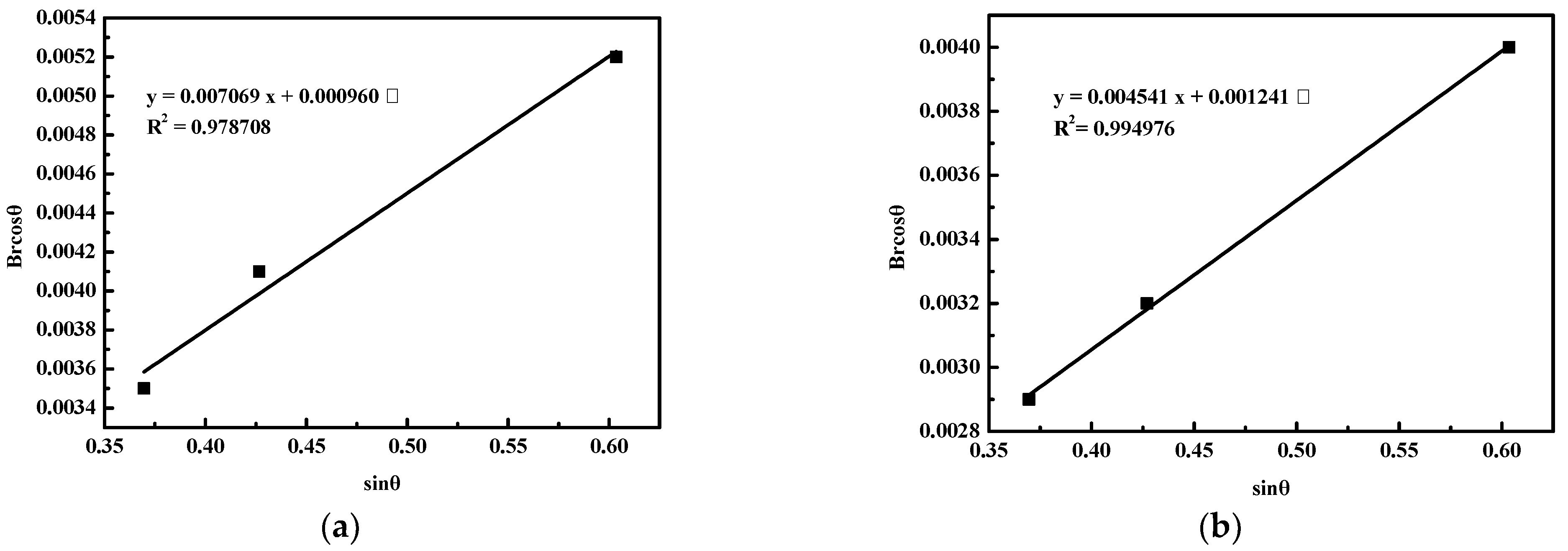
Figure 5a,b present Williamson and Hall plots for the as-deposited and annealed samples, respectively. A linear fit was applied to the scattered data points. From this linear fit, the crystallite size can be estimated from the y-intercept, and the strain can be determined from the slope of the fit. The lattice strain is calculated by comparing the linear fit equations with the equation B
rcosθ = kλ/(L) + ηsinθ for both the as-deposited and annealed samples. The lattice strains obtained for the as-deposited and annealed samples were measured as 0.007069 and 0.004541, respectively. To estimate the degree of stress, the Young’s modulus of copper was considered. The reported values for the Young’s modulus of copper in different studies vary slightly. For polycrystalline copper, the bulk modulus is approximately 130 GPa, while Yu and Spaepen reported that the Young’s modulus of a Cu thin film on Kapton was 108.8 GPa [
28]. In other studies, Read et al. reported micro-tensile-test results for electrodeposited copper that was 2.59 μm thick and tested at 25 °C. The average value of the Young’s modulus was 73 ± 24 GPa. [
29]. Yang et al. demonstrated that the Young’s modulus (E) values of electroplated Cu were measured to be 106.4 (±13.0) GPa; in their study, these values was examined using a nano-indenter with a three-sided pyramidal Berkovich diamond indenter [
30]. The Young’s modulus of Cu thin film is 108.8 GPa, which was selected to estimate the stress. In this analysis, Young’s modulus of Cu thin film was assumed to be 108.8 GPa. Based on this value, the stresses were calculated as 76.4 MPa for the as-deposited sample and 49.1 MPa for the annealed sample. It is worth noting that the residual stresses of both samples fall within the MPa range and are below 100 MPa.
In the study conducted by Lee et al., stress measurements were performed using XRD. They found that at a film thickness of 2.5 μm, the residual stresses were approximately 630 MPa for the as-plated sample and 110 MPa for the self-annealed sample. During self-annealing, an average stress release of 500 MPa was observed in the electroplated samples [
15]. In another study by Lassnig et al., magnetron sputtering was used to deposit 110 nm thin Cu films on glass substrates. The residual stresses were determined using synchrotron radiation. For the as-deposited films at 0.5 Pa, residual stresses of (120 ± 17) MPa were measured, and after annealing, an increase in stress up to (310 ± 24) MPa was observed [
21]. Through the comparison of the reported values and the results obtained in this study, it was determined that the observed residual stress levels for the copper film in this study are lower than those reported by Lee et al. [
15] and Lassnig et al. [
21]. In this study, the as-deposited sample exhibited higher residual stress than the annealed sample. The lattice strain, which is indicative of the distribution of lattice constants and lattice dislocations arising from crystal imperfections, showed a decrease in the material after thermal annealing. The higher tension observed in the as-deposited sample compared to the annealed sample can be attributed to the lattice structure variations induced by thermal annealing. These variations may decrease lattice strain within a material, leading to a reduction in residual stress.
The peeling of materials is a common technique used to characterize material properties, particularly with respect to adhesives and interfaces. Peel tests have been widely developed, standardized, and employed in order to assess various properties of materials, adhesives, and interfaces. [
31]. A critical aspect of peel tests is their ability to evaluate interfacial adhesion failure, which refers to fracturing occurring at the interface between two materials. Analyzing the peeling process and employing relevant equations facilitate the measurement of the fracture energy of both bulk materials and adhesive interfaces. The peel test is favored for its relative simplicity, as it separates a layer from a substrate. It is often one of the initial methods employed to characterize the adhesion properties of thin films. Due to its straightforward and fast nature, the peel test is commonly used to determine the adhesion strength of interconnector ribbons to solar cell metallizations. In the context of crystalline silicon solar cells, the peel test is often the initial test conducted to qualify the interconnection of these cells after soldering. This test involves peeling off the interconnector ribbons from the solar cell, and the force required for peeling is measured. The peel test is an easy and fast method for assessing the strength of the adhesion of interconnector ribbons to a solar cell. The test can determine whether the adhesion meets the required specifications by measuring the force required for peeling. This allows for the acceptance or rejection of new cells in a module production line, ensuring that only cells with satisfactory interconnection adhesion are used. In this context, the peel test plays a crucial role in quality control and ensuring the reliability of solar cell modules. It provides a quick and effective means of evaluating the interconnection adhesion, helping maintain the solar cell modules’ desired performance and durability [
32]. In this study, tape and peel-off tests were employed to evaluate the adhesion of electroplated copper on the Cu(s)/ITO/Si substrate. Both tests were conducted on the as-deposited and annealed samples. During the tape test, adhesive tape was applied to the surface of the samples and then rapidly removed. For both the as-deposited and annealed samples, the electroplated copper layer remained intact on the Cu(s)/ITO/Si substrate after the tape test. This indicates a high level of adhesion strength for both samples. However, it is essential to note that the tape test does not provide a quantitative measurement of adhesion strength. To obtain a quantitative measure of the adhesion strength of the electroplated copper on Cu(s)/ITO/Si, the peel-off test was performed using a universal testing machine. This test involves applying a controlled force to peel off the electroplated copper layer from the substrate. The adhesion strength can be quantitatively determined by measuring the energy required to initiate and propagate the peeling. The peel-off test provides a more accurate and quantitative assessment of adhesion strength compared to the tape test. It allows for a more precise understanding of the bonding between the electroplated copper layer and the Cu(s)/ITO/Si substrate, providing valuable information for evaluating the quality and reliability of the electroplated copper film in this materials system.
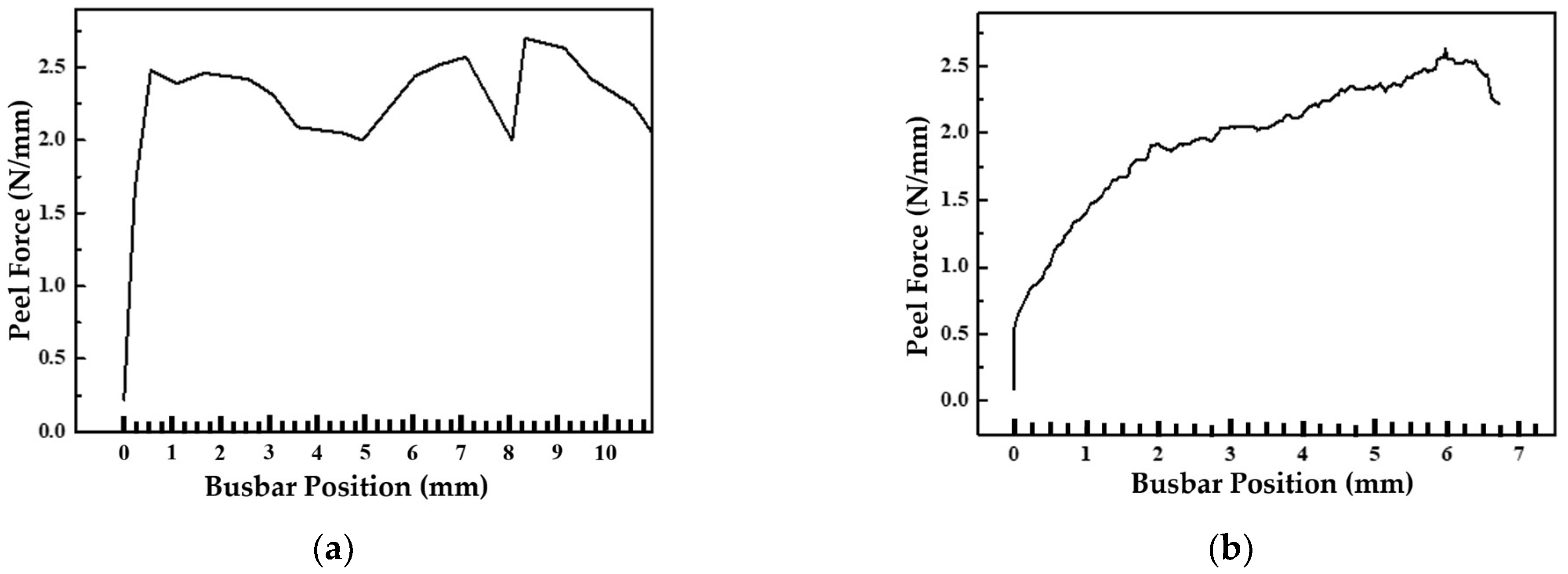
Figure 6a,b present the peel force diagrams for the as-deposited and annealed samples. The maximum peel force value for the as-deposited sample was 2.63 N/mm, while the average peel force was 2.25 N/mm. As for the annealed sample, the highest peel force value was 2.57 N/mm, and the middle peel force value was 2.25 N/mm. These results indicate strong adhesion between the electroplated copper and the Cu(s)/ITO/Si substrate, and the adhesion strength appears to be independent of heat treatment. Notably, neither sample had copper remaining on the ITO/Si substrate after the 90° peel-off test. In a study conducted by Yu et al., the authors investigated the interface between copper and SHJ (Silicon Heterojunction) solar cells, using SEM (Scanning Electron Microscopy) to examine the cross-sectional morphology. They observed micro-voids at the interface between the electroplating copper layer and the copper seed layer and the interface between the copper seed layer and the TCO layer. They found that solar cells with poor peel force exhibited deteriorated adhesion due to the presence of these voids. The authors attributed the formation of voids to the partial corrosion of the copper seed layer in a copper sulfate solution with a very low pH (hydrogen ion concentration) [
33]. In contrast, in the current study, no voids were observed at the interface between the copper seed and ITO layers, and it was difficult to detect any voids at the interface between the electroplating copper and the copper seed layer. The high adhesion strength observed in this study can be attributed to the absence of gaps or voids at the interface between the electroplated copper and the copper seed layer.
