Article

Atomic Layer Deposited SiOX-Based Resistive Switching Memory for Multi-Level Cell Storage

1
Division of Electronics and Electrical Engineering, Dongguk University, Seoul 04620, Korea
2
Department of Electrical and Computer Engineering, Seoul National University, Seoul 151742, Korea
*
Authors to whom correspondence should be addressed.
These authors contributed equally to this work.
Metals 2022, 12(8), 1370; https://doi.org/10.3390/met12081370
Submission received: 13 July 2022 / Revised: 31 July 2022 / Accepted: 15 August 2022 / Published: 18 August 2022
(This article belongs to the Special Issue Metal Oxides Characterization for Emerging Memory Device Applications)

Abstract

:
Herein, stable resistive switching characteristics are demonstrated in an atomic-layer-deposited SiOX-based resistive memory device. The thickness and chemical properties of the Pt/SiOX/TaN stack are verified by transmission electron microscopy (TEM) and X-ray photoemission spectroscopy (XPS). It is demonstrated that much better resistive switching is obtained using a negative set and positive reset compared to the opposite polarity. In addition, multi-level switching is demonstrated by changing the compliance current (CC) and the reset stop voltage, and potentiation and depression are emulated by applying pulses to achieve a synaptic device. Finally, a pulse endurance of 10,000 cycles and a retention time of 5000 s are confirmed by modulating the pulse input and reading voltage, respectively.

1. Introduction

For non-volatile memory (NVM) applications, resistive random-random access memory (RRAM) has several advantages, such as a simple metal–insulator–metal (MIM) structure, superior storage capacity with small component size, fast switching speed, low power consumption, non-volatility, multi-level data storage ability, and long retention time [1,2,3,4,5,6,7]. In particular, RRAM has the potential to implement multiple conductive levels in one cell, thereby facilitating a high storage density by the implementation of multiple bits in the NVM [8,9,10], and has made possible the quasi-analog modulation of synaptic weight in the artificial neural network (ANN) [11,12,13,14,15,16,17]. Furthermore, RRAM can solve the various disadvantages of dynamic random-access memory (DRAM) and flash memory. For instance, DRAM has volatile characteristics when processing data quickly [18], whereas flash memory is non-volatile but exhibits slow data processing and requires high voltage operation [19].
Due to the above-mentioned advantages, RRAM has been used to implement a neuromorphic computing architecture [11,12,13,14,15,16,17]. The importance of neuromorphic computing architecture begins with solving the bottleneck problem caused by the use of a data bus for data exchange in the von Neumann architecture. This problem has emerged in recent years due to the increased amount of data to be processed in artificial intelligence (AI) development. The neuromorphic computing architecture can solve this problem by imitating the human brain structure in order to process data in parallel with low power consumption. While various novel resistance-based memory devices are attracting attention for the implementation of the neuromorphic computing architecture, including phase-change random-access memory (PRAM) [20] and magnetic random-access memory (MRAM) [21], the RRAM devices are particularly attractive due to their above-mentioned advantages.
To obtain reliable resistive switching characteristics with small variation, the thickness of the RRAM device should be uniform. In this respect, the self-limiting process of atomic layer deposition (ALD) enables the fabrication of thin films with very exact thicknesses and is especially suitable for the vertical RRAM structure [22]. In the present work, the multi-level cell (MLC) characteristics of an ALD-fabricated Pt/SiOX/TaN device are examined via I-V curves and pulse modulation. In addition, the thickness of the stack device is estimated via transmission electron microscopy (TEM). Further, the MLC characteristics are observed by varying the compliance current (CC) and reset stop voltage in direct-current (DC) sweep mode, and high endurance is demonstrated by the pulse response.

2. Experiments

The RRAM samples were fabricated using the following procedures. A 100-nm thick TaN bottom electrode was deposited by reactive sputtering onto the SiO2/Si substrate. The SiOx was deposited via the following sequential ALD protocol: di-isopropylaminosilane (SiH3N (C3H7)2, DIPAS), 0.8 s; N2 purge, 15 s; ozone (O3) 0.5 s; N2 purge, 15 s, with a total of 40 cycles at a stage temperature of 450 °C. Finally, a 100-nm thick Pt top electrode was deposited via e-beam evaporation with a shadow mask containing a pattern of circles with a diameter of 100 μm. The chemical and material characteristics of the ALD-deposited SiOX film were examined via X-ray photoelectron spectroscopy (XPS). The electrical characteristics of the RRAM cells were measured and recorded using a semiconductor parameter analyzer (Keithley 4200-SCS and 4225-PMU ultrafast module) in the voltage sweep and pulse modes with the bottom electrode grounded and a bias applied to the top electrode.

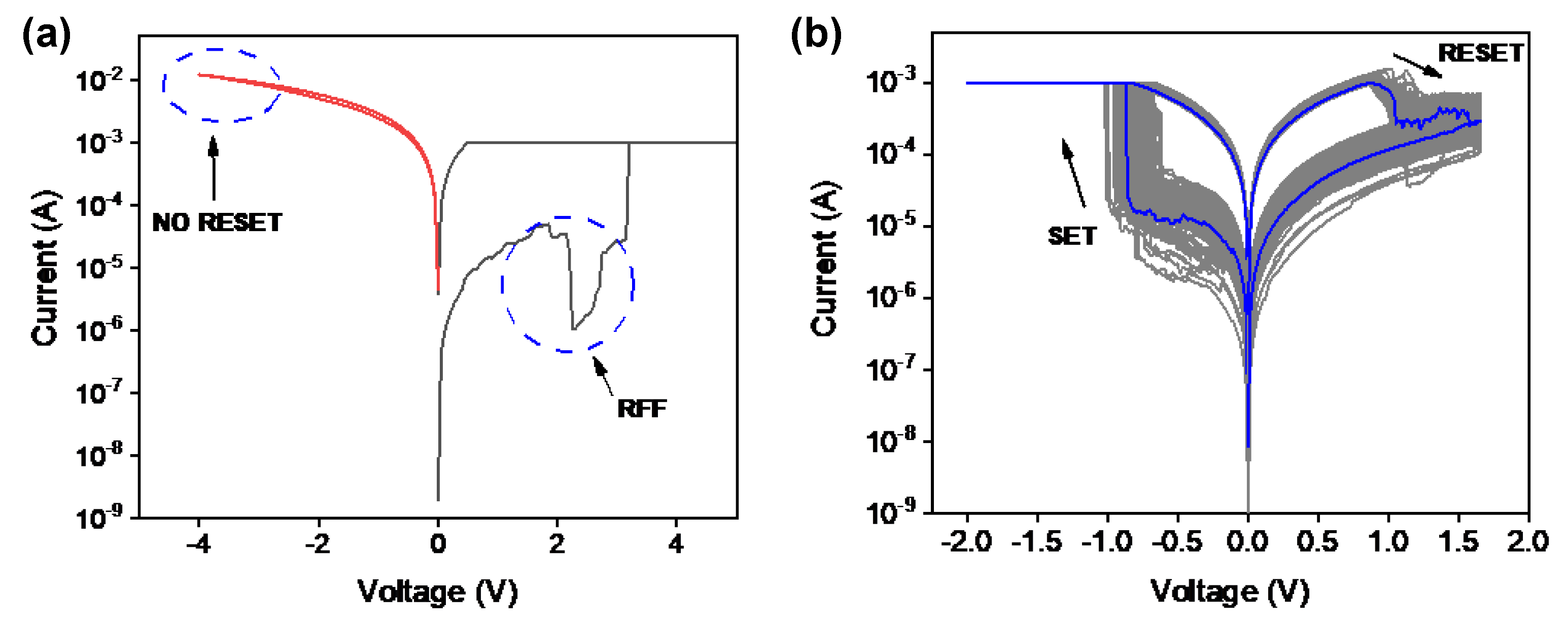
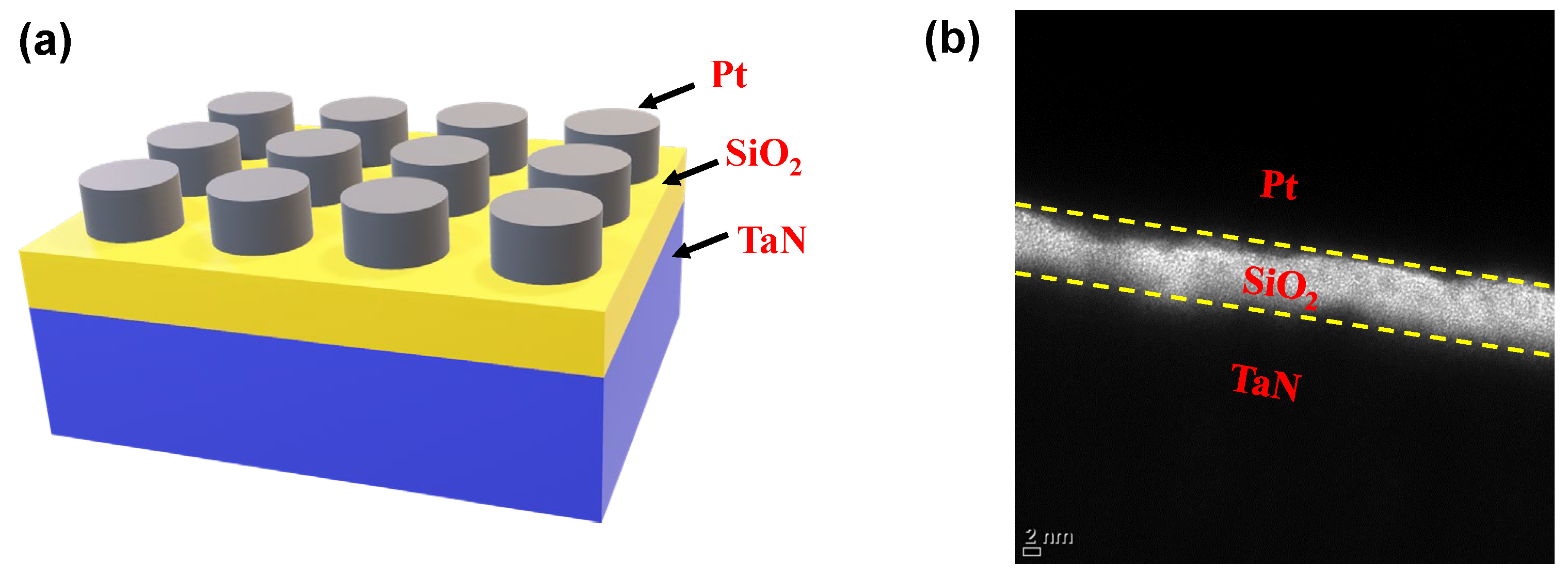
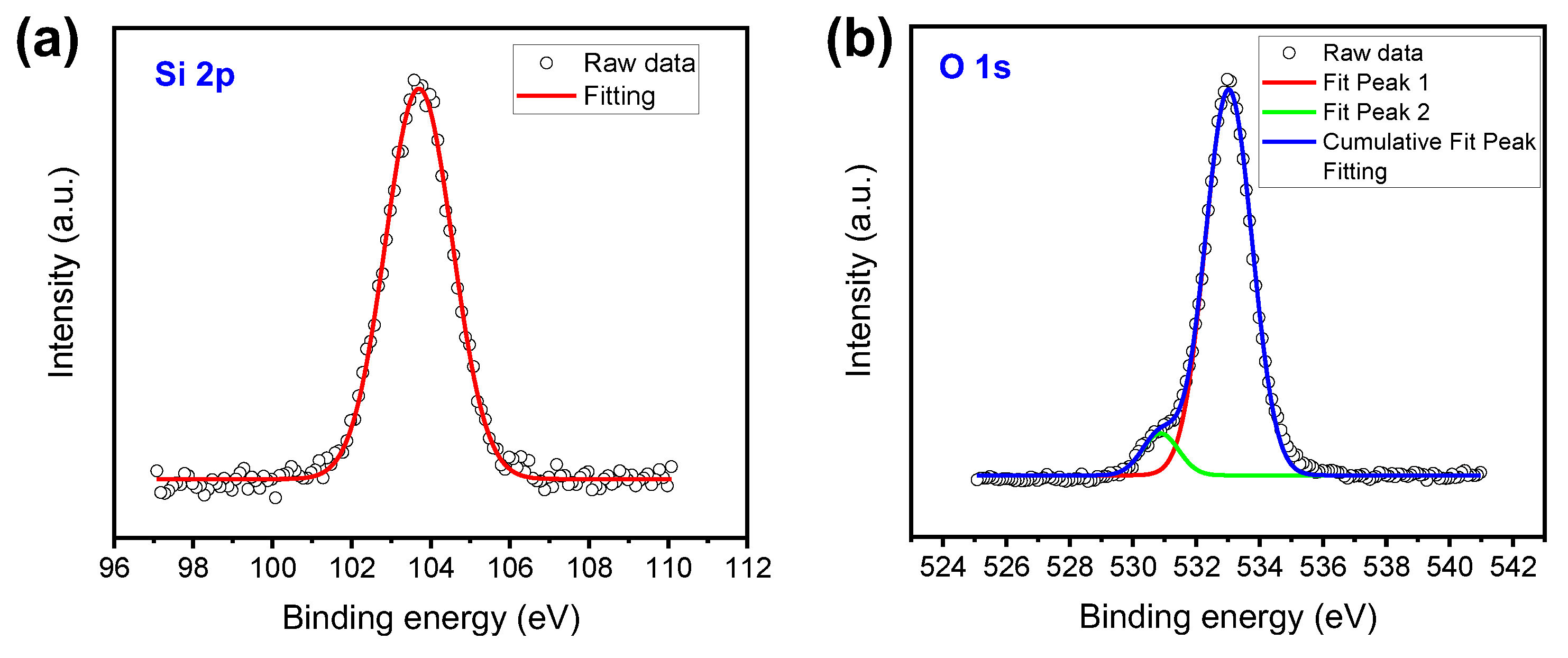
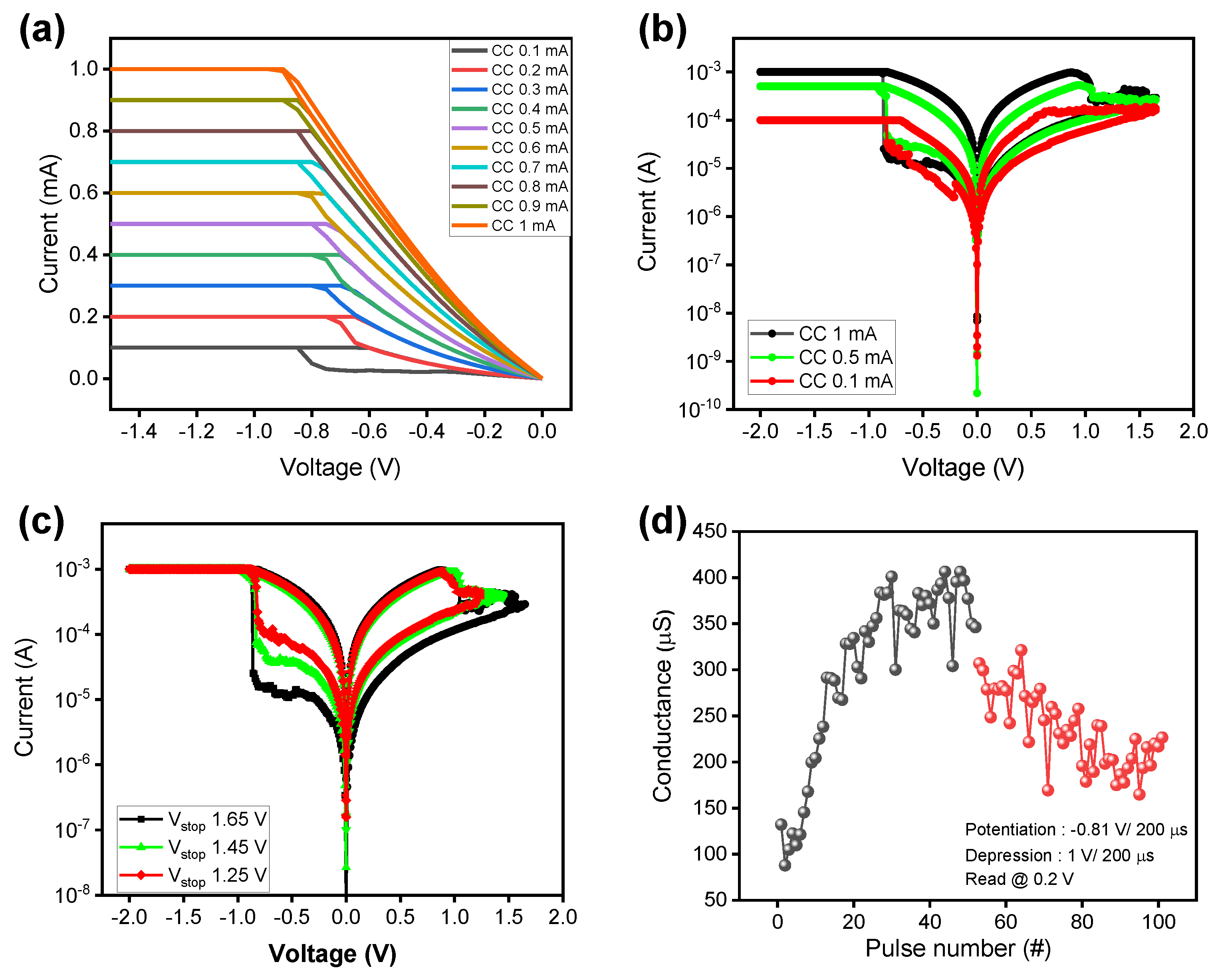
3. Results and Discussion

A schematic diagram of the Pt/SiOX/TaN RRAM structure is presented in Figure 1a, where multiple Pt electrodes are separated from each other to provide independent memory cells while the insulating SiOX film covers the entire TaN surface. The TEM image in Figure 1b reveals a thickness of ~6 nm for the amorphous SiOX layer. The interface of SiOx on the TaN layer is rather rough even though SiOx was deposited by ALD. The XPS core level Si 2p spectrum of the SiOX film is presented in Figure 2a. Here, the peak centered at a binding energy of 103.7 eV corresponds to the non-stoichiometric Si–O bond [23]. Meanwhile, the O 1s spectrum in Figure 2b exhibits two peaks centered at 530.87 eV and 533.02 eV [23]. A further peak corresponding to the non-stoichiometric Si–O bond was also observed at higher binding energy.
The resistive switching characteristics of the device in the DC sweep mode according to operation polarity are presented in Figure 3. In the positive forming process (Figure 3a), the I-V curve reveals reverse filament formation (RFF) during the first switching. This indicates that conducting filaments with sufficient defects are initially formed in the SiOX, and these can be ruptured upon application of a bias. The ruptured filament can reform with a sudden rise in current during the set process, but the subsequent reset process does not occur fluently because the Pt electrode does not contain enough oxygen. By contrast, stable bipolar resistive switching is achieved by using a negative set and positive reset voltage, as shown in Figure 3b. Here, the set process is accompanied by a sharp rise in current within a set voltage range of −0.61 V to −1.02 V, thus indicating the formation of conducting filaments in the SiOX layer. Subsequently, the reset process begins at ~0.92 V, and the current gradually decreases over a wide voltage range. This indicates that the filament is only gradually ruptured, which is suitable for voltage-controlled MLC applications. The detailed switching and conduction mechanisms of SiOx-based RRAM were explained by previous literature [24,25].
The MLC characteristics of the Pt/SiOX/TaN RRAM device are implemented by varying the compliance current and the reset stop voltage, as shown in Figure 4. Thus, in Figure 4a, the compliance current is increased from 0.1 to 1.0 mA in increments of 0.1 mA, and the currents in both the low and high resistance states are seen to increase with increasing compliance current. This demonstrates that the size of the conducting filament can be successfully controlled by modulating the compliance current.
The bipolar resistive switching (set/reset) characteristics obtained by controlling the compliance current only are presented in Figure 4b. Here, the low-resistance state is effectively changed by changing the compliance current, but no obvious change is observed in the high-resistance state. Meanwhile, the I-V curves obtained by varying only the reset stop voltage for the same compliance current are presented in Figure 4c. Here a significant variation in the high resistance state is observed according to the reset stop voltage. The MLC characteristics are then further demonstrated for practical memory operation by the application of multiple sets and reset pulses of −0.81 V and +1 V (Figure 4d). To minimize the read disturbance, a read voltage of 0.2 V was used to obtain the conductance values. Thus, while there is some variability, the conductance exhibits an overall increase with 50 negative pulses and an overall decrease with 50 positive pulses. Thus, it is possible to increase and decrease the conductance of the RRAM device by imitating the potentiation and depression processes that strengthen and weaken the connections between biological synapses. This MLC process is, therefore, suitable for hardware-based neuromorphic systems.
Finally, the stable endurance and retention characteristics of the Pt/SiOX/TaN RRAM device for reliable non-volatile memory applications are demonstrated in Figure 5. The conductance values of the high and low resistance states during cyclic application of the set (−3 V) and reset (4 V) pulses, with a read voltage of −1 V, are presented in Figure 5a. Here, good pulse endurance is demonstrated for up to 10,000 cycles with an on/off ratio of about 4. The time-dependent data-retention properties are indicated in Figure 5b, where the high and low resistance states were obtained by a DC sweep. Here, both resistance states are maintained without significant degradation for 5000 s, thereby demonstrating that the Pt/SiOX/TaN device has non-volatile memory properties.

4. Conclusions

Herein, the resistive switching of an atomic-layer-deposited (ALD) SiOX-based resistive random-random access memory (RRAM) device was demonstrated for mutli-level cell (MLC) storage. The thickness and chemical properties of the device were investigated by transition electron microscopy (TEM) and X-ray photoelectron spectroscopy (XPS), respectively. Bipolar resistive switching was shown to occur more easily under a negative set and positive reset operation than in the opposite polarity due to oxygen exchange in the TiN layer. For MLC, the compliance current and reset stop voltage were used to control the low and high resistance values. In addition, for neuromorphic applications, potentiation and depression were demonstrated by pulse application. Finally, the retentions of the high and low resistance states were verified for 5000 s and 10,000 cycles of alternating current (AC) endurance.

Author Contributions

J.S., G.N. and S.K. (Sungjoon Kim) conducted the electrical measurements and process, and Y.L. and D.C. wrote the manuscript; J.J. and S.K. (Sungjun Kim) supervised the study. All authors have read and agreed to the published version of the manuscript.

Funding

Dongguk University Research Fund of 2020 and Korea Institute of Energy Technology Evaluation and Planning (KETEP) grant funded by the Korea government (MOTIE) under Grant 20224000000020.

Data Availability Statement

Not applicable.

Conflicts of Interest

The authors declare no conflict of interest.

References

  1. Sawa, A. Resistive switching in transition metal oxides. Mater. Today 2008, 11, 28–36. [Google Scholar] [CrossRef]
  2. Lee, M.-J.; Lee, C.B.; Lee, D.; Lee, S.R.; Chang, M.; Hur, J.H.; Kim, Y.-B.; Kim, C.-J.; Seo, D.H.; Seo, S.; et al. A fast, high-endurance and scalable non-volatile memory device made from asymmetric Ta2O(5-x)/TaO(2-x) bilayer structures. Nat. Mater. 2011, 10, 625–630. [Google Scholar] [CrossRef] [PubMed]
  3. Bai, Y.; Wu, H.; Wu, R.; Zhang, Y.; Deng, N.; Yu, Z.; Qian, H. Study of Multi-level Characteristics for 3D Vertical Resistive Switching Memory. Sci. Rep. 2014, 4, 7359. [Google Scholar] [CrossRef]
  4. Hsu, C.W.; Wang, Y.F.; Wan, C.C.; Wang, I.T.; Chou, C.T.; Lai, W.L.; Lee, Y.J.; Hou, T.H. Homogeneous barrier modulation of TaOX/TiO2 bilayers for ultra-high endurance three-dimensional storage-class memory. Nanotechnology 2014, 25, 165202. [Google Scholar] [CrossRef]
  5. Mikhaylov, A.; Belov, A.; Korolev, D.; Antonov, I.; Kotomina, V.; Kotina, A.; Gryaznov, E.; Sharapov, A.; Koryazhkina, M.; Kryukov, R.; et al. Multilayer Metal-Oxide Memristive Device with Stabilized Resistive Switching. Adv. Mater. Technol. 2020, 5, 1900607. [Google Scholar] [CrossRef]
  6. Sun, C.; Lu, S.; Jin, F.; Mo, W.; Song, J.; Dong, K. The Resistive Switching Characteristics of TiN/HfO2/Ag RRAM Devices with Bidirectional Current Compliance. J. Electron. Mater. 2019, 48, 2992–2999. [Google Scholar] [CrossRef]
  7. Matveyev, Y.; Egorov, K.; Markeev, A.; Zenkevich, A. Resistive switching and synaptic properties of fully atomic layer deposition grown TiN/HfO2/TiN devices. J. Appl. Phys. 2015, 117, 044901. [Google Scholar] [CrossRef]
  8. Kim, S.; Abbas, Y.; Jeon, Y.R.; Sokolov, A.S.; Ku, B.; Choi, C. Engineering synaptic characteristics of TaOX/HfO2 bi-layered resistive switching device. Nanotechnology 2018, 29, 415204. [Google Scholar] [CrossRef]
  9. Oh, I.; Pyo, J.; Kim, S. Resistive Switching and Synaptic Characteristics in ZnO/TaON-Based RRAM for Neuromorphic System. Nanomaterials 2022, 12, 2185. [Google Scholar] [CrossRef]
  10. Kim, S.T.; Cho, W.J. Improvement of multi-level resistive switching characteristics in solution-processed AlOX-based non-volatile resistive memory using microwave irradiation. Semicond. Sci. Technol. 2017, 33, 015009. [Google Scholar] [CrossRef]
  11. Yang, J.J.; Strukov, D.B.; Stewart, D.R. Memristive devices for computing. Nat. Nanotechnol. 2013, 8, 13. [Google Scholar] [CrossRef] [PubMed]
  12. Kim, C.-H.; Lim, S.; Woo, S.Y.; Kang, W.M.; Seo, Y.-T.; Lee, S.T.; Lee, S.; Kwon, D.; Oh, S.; Noh, Y. Emerging memory technologies for neuromorphic computing. Nanotechnology 2018, 30, 032001. [Google Scholar] [CrossRef] [PubMed]
  13. Mikhaylov, A.; Pimashkin, A.; Pigareva, Y.; Gerasimova, S.; Gryaznov, E.; Shchanikov, S.; Zuev, A.; Talanov, M.; Lavrov, I.; Demin, V.; et al. Neurohybrid Memristive CMOS-Integrated Systems for Biosensors and Neuroprosthetics. Front. Mol. Neurosci. 2020, 14, 358. [Google Scholar] [CrossRef] [PubMed]
  14. Lobov, S.A.; Mikhaylov, A.N.; Shamshin, M.; Makarov, V.A.; Kazantsev, V.B. Spatial Properties of STDP in a Self-Learning Spiking Neural Network Enable Controlling a Mobile Robot. Front. Neurosci. 2020, 14, 88–97. [Google Scholar] [CrossRef] [PubMed]
  15. Emelyanov, A.V.; Nikiruy, E.K.; Serenko, A.V.; Sitnikov, A.V.; Presnyakov, M.Y.; Rybka, R.B.; Sboev, A.G.; Rylkov, V.V.; Kashkarov, P.K.; Kovalchuk, M.V.; et al. Self-adaptive STDP-based learning of a spiking neuron with nanocomposite memristive weights. Nanotechnology 2019, 31, 045201. [Google Scholar] [CrossRef]
  16. Demin, V.; Nekhaev, D.; Surazhevsky, I.; Nikiruy, K.; Emelyanov, A.; Nikolaev, S.; Rylkov, V.; Kovalchuk, M. Necessary conditions for STDP-based pattern recognition learning in a memristive spiking neural network. Neural Netw. 2020, 134, 64–75. [Google Scholar] [CrossRef] [PubMed]
  17. Emelyanov, A.; Nikiruy, K.; Demin, V.; Rylkov, V.; Belov, A.; Korolev, D.; Gryaznov, E.; Pavlov, D.; Gorshkov, O.; Mikhaylov, A.; et al. Yttria-stabilized zirconia cross-point memristive devices for neuromorphic applications. Microelectron. Eng. 2019, 215, 110988. [Google Scholar] [CrossRef]
  18. Okhonin, S.; Nagoga, M.; Sallese, J.M.; Fazan, P. A capacitor-less 1T-DRAM cell. IEEE Electron. Device Lett. 2002, 23, 85–87. [Google Scholar] [CrossRef]
  19. Lu, C.-Y.; Hsieh, K.-Y.; Liu, R. Future challenges of flash memory technologies. Microelectron. Eng. 2009, 86, 283–286. [Google Scholar] [CrossRef]
  20. Jiao, F.; Chen, B.; Ding, K.; Li, K.; Wang, L.; Zeng, X.; Feng, R. Monatomic 2D phase-change memory for precise neuromorphic Computing. Appl. Mat. Today 2020, 20, 100641. [Google Scholar] [CrossRef]
  21. Bishnoi, R.; Ebrahimi, M.; Oboril, F.; Tahoori, M.B. Improving Write Performance for STT-MRAM. IEEE Trans. Magn. 2016, 52, 1–11. [Google Scholar] [CrossRef]
  22. Fang, Y.; Yu, Z.; Wang, Z.; Zhang, T.; Yang, Y.; Cai, Y.; Huang, R. Improvement of HfOX-Based RRAM Device Variation by Inserting ALD TiN Buffer Layer. IEEE Electron. Device Lett. 2018, 39, 819–822. [Google Scholar] [CrossRef]
  23. Arl, D.; Rogé, V.; Adjeroud, N.; Pistillo, B.R.; Sarr, M.; Bahlawane, N.; Lenoble, D. SiO2 thin film growth through a pure atomic layer deposition technique at room temperature. RSC Adv. 2020, 10, 18073–18081. [Google Scholar] [CrossRef] [PubMed]
  24. Chang, Y.-F.; Fowler, B.; Chen, Y.-C.; Chen, Y.-T.; Wang, Y.; Xue, F.; Zhou, F.; Lee, J.C. Intrinsic SiOx-based unipolar resistive switching memory. II. Thermal effects on charge transport and characterization of multilevel programing. J. Appl. Phys. 2014, 116, 043709. [Google Scholar] [CrossRef]
  25. Mehonic, A.; Cueff, S.; Wojdak, M.; Hudziak, S.; Jambois, O.; Labbe, C.; Garrido, B.; Rizk, R.; Kenyon, A.J. Resistive switching in silicon suboxide films. J. Appl. Phys. 2012, 111, 074507. [Google Scholar] [CrossRef]
Figure 1. A schematic diagram (a) and cross-sectional TEM image (b) of the Pt/SiOX/TaN RRAM device.
Metals 12 01370 g001
Figure 2. The XPS core level spectra of the ALD deposited SiOX film: (a) Si 2p; (b) O 1s.
Metals 12 01370 g002
Figure 3. The I-V characteristics of the Pt/SiOX/TaN RRAM device under (a) positive set and negative reset operation, and (b) negative set and positive reset operation.
Metals 12 01370 g003
Figure 4. The MLC characteristics of the Pt/SiOX/TaN RRAM device: (a) plots of the low-resistance current with various compliance currents; (b and c) controlling the bipolar resistive switching via (b) the compliance current and (c) the reset stop voltage; (d) potentiation (black) and depression (red) by the application of negative and positive pulses, respectively.
Metals 12 01370 g004
Figure 5. (a) Pulse endurance and (b) and retention properties of the Pt/SiOX/TaN RRAM device.
Metals 12 01370 g005
Publisher’s Note: MDPI stays neutral with regard to jurisdictional claims in published maps and institutional affiliations.

