Abstract
The low melting temperature In-48Sn alloy is a promising candidate for flexible devices. However, the joint strength of the In-48Sn alloy on the Cu substrate was low due to the rapid diffusion of Cu into the In-rich alloy. In this study, the effect of the addition of xCu (x = 2.0 and 8.0 wt.%) on wettability, interfacial reaction, and mechanical strength of the In-Sn-xCu/Cu joint is analyzed. The results demonstrate that both the In-48Sn and In-Sn-xCu alloys exhibit good wettability on the Cu substrate and that the contact angle increases with an increase in the Cu content. Furthermore, fine grains are observed in the alloy matrix of the In-Sn-xCu/Cu joint and the interfacial intermetallic compound (IMC) comprising the Cu-rich Cu6(In,Sn)5 near the Cu substrate and the Cu-deficient Cu(In,Sn)2 near the solder side. The In-Sn-2.0Cu/Cu joint with fine microstructure and a small amount of IMC in the alloy matrix shows the highest average shear strength of 16.5 MPa. Although the In-Sn-8.0Cu/Cu joint also exhibits fine grains, the presence of large number of voids and rough interfacial IMC layer causes the formation of additional stress concentration points, thereby reducing the average shear strength of the joint.
1. Introduction
Electronic devices have become lighter, bendable, and stretchable owing to miniaturization and use of flexible substrates [1,2,3,4]. Reliability of solder joints is very important for the effective operation of electrical components as solder joints provide both electrical and mechanical integration between the components [5]. Tin–lead (Sn-Pb) alloy is the most widely used solder in electronic packaging because of its low cost, good wettability, acceptable electrical conductivity, and good mechanical properties [6]. In recent years, the Sn-Pb alloy has been replaced by Pb-free alloys, such as Sn-Au, Sn-Ag-Cu, Sn-Cu, Sn-Ag, Sn-Bi, and Sn-In, owing to the toxicity of Pb [7,8,9,10,11]. Most of the Pb-free alloys have higher melting temperatures (Tm) than the eutectic Sn-37Pb alloy (183 °C), e.g., Sn-3.5Ag (Tm = 221 °C), Sn-3.0Ag-0.5Cu (Tm = 217 °C), and Sn-9Zn (Tm = 198 °C), [7,12]. However, an alloy with a higher melting temperature exhibits a higher peak reflow temperature, which causes thermal damage and excessive warpage owing to the mismatch in coefficient of thermal expansion (CTE) between the electric component and the substrate. This affects the reliability of the solder joint. Therefore, studies on low-melting-temperature alloys and their joint reliabilities are necessary. According to JIS Z 3282:2017, the solidus temperature of low-meting-temperature alloys is less than 150 °C. Among the Pb-free alloys, Sn-58Bi (Tm = 138 °C), and In-48Sn (Tm = 118 °C), are the most promising candidates for low-temperature soldering applications [8,9,10,11]. However, the eutectic Sn-58Bi alloy with a reflow temperature of 180 °C [13,14] is not suitable for substrates (in flexible electronics) that require a low operating temperature (<180 °C), such as heat-stabilized polyethylene terephthalate and heat-stabilized polyethylene naphthalate [1,2,15]. The In-48Sn alloy with a low Tm (118 °C), high ductility, and good wettability [16,17,18,19] is a promising candidate for flexible electronic devices that use substrates with low melting temperatures [20,21]. However, in order to serve the function of joining electronic components to a printed wiring board circuit, solder alloys are used at high homologous temperatures (usually exceeding 0.5Tm of the alloy). At this temperature, diffusion processes are very active, creep strain will be induced in addition to the plastic deformation [22,23]. When expressed in Kelvins, the homologous temperature (Th) of the In-48Sn alloy at room temperature (T~25 °C~298 K) is approximately 0.76 (Th = T/Tm = 298 K/391 K = 0.76). As a result, the microstructure of solder alloys is unstable at normal operating, and storage temperatures for electronic equipment. These changes, in turn, influence the mechanical properties and in-service performance of a solder alloy, which lead to failure of components caused by long-term temperature load and/or multiple temperature cycling loads [24,25]. It has been reported that 52In-48Sn alloy has a lower isothermal fatigue resistance than 58Bi-42Sn alloy but withstands fatigue better than 43Sn-43Pb-14Bi alloy after 6000 cycles of thermal shock test [26]. The low mechanical strength and low creep resistance [17] limit applicability of In-48Sn alloy as a low-temperature solder. Therefore, several studies have focused on improving the mechanical properties of In-Sn bulk alloys by adding trace elements such as Zn, Bi, Ag, and Cu [10,20,27,28]. For instance, it has been indicated that Cu is conducive to improving the performance of Sn-Zn solder alloys [29,30]. Moreover, Jun Shen reported that Cu addition decreased melting point and refined microstructure, which resulted in an increase in both ultimate tensile strength and ductility of Sn-Bi-based alloy [31]. Development of Pb-free alloys using high Cu content (4–20 wt.%) has been carried out by several researchers [32,33,34,35,36]. Among them, Li Yang et al. [36] studied microstructure evolution and shear strength of solder joint using In-Sn-20Cu composite particles by transient liquid phase (TLP) bonding. They found that the maximum shear strength is 26.54 MPa when the bonding time is 15 min, bonding stress of 3 MPa, and the bonding temperature of 260 °C. The result revealed that although Cu addition can improve the strength of In-Sn-based solder joint, a high content of Cu led to the high bonding temperature which is not suitable for low melting temperature substrates in flexible electronics. Relatively few studies have investigated the effect of Cu on In-Sn alloy [37,38]. It has been reported that a low Cu content addition (0.35–1.5 wt.% Cu) remained melting temperature of In-Sn alloy, and a ternary Cu2In3Sn IMC was observed in the as-solidified alloy [37]. However, the effect of Cu on the mechanical properties of eutectic In-Sn alloy has not been mentioned. To date, very little research has been conducted on alloys with high Cu content for low-temperature applications. Therefore, in our previous study [20], we selected Cu as an additional element into the InSn alloy with the expectation that it will help in maintaining or reducing the melting temperature and improving the mechanical properties of this alloy. We found that the elongation of In-48Sn bulk alloy was enhanced by a factor of approximately 2.0 and the tensile strength was enhanced by a factor of approximately 1.5 with the addition of 2.0 and 8.0 wt.% Cu, respectively. It is noted that a higher elastic moduli solder alloys tend to transfer more thermal stresses from the substrate to the devices, which leads to fatigue failure in solder joint during operation. Therefore, joining materials with a lower elastic modulus are beneficial in making a more reliable joint between the device and substrate, especially for application in flexible electronics [39]. To better understand the properties of the new In-Sn-Cu alloys, further discussion about the elastic modulus of the alloys and specific research on the strength and microstructure of alloy joint are essential.
Recently, some researchers have analyzed the interfacial reactions between eutectic In-Sn alloys and different substrates, such as Cu and Ni/Cu [16], Au [40], Nb [41], and electroless Ni/immersion Au [19,42]. For example, the interfacial layer between the In-Sn-based alloy and the Cu substrate consists of two compounds, namely, the Cu-rich Cu2(In,Sn) near the Cu side and the In-rich Cu2In3Sn near the alloy side [17,43]. Chuang et al. [18] reported that during the soldering of the In-49Sn/Cu joint at temperatures of 150–400 °C, a planar ε-Cu3(In,Sn) layer and an elongated scalloped η-Cu6(In,Sn)5 structure are formed at the Cu substrate side and the alloy side of the In-49Sn/Cu interface, respectively. Although the In-Sn eutectic alloy exhibited a good contact angle with an equilibrium value of 25°, the joint strength of the In-Sn alloy on the Cu substrate was low because of the rapid diffusion of Cu into the In-rich alloy during the reflow process [17,18]. Furthermore, Sommadossi et al. found that η-Cu6(Sn,In)5 intermetallic compounds (IMCs) are formed on the Cu side and Cu2(In,Sn) IMCs are formed at the Cu/In-48Sn/Cu interface after diffusion soldering at temperatures 200–400 °C and a low pressure between 0.5 and 5 MPa [44]. The results of previous works imply that the interfacial reactions between the In-Sn alloy and the Cu substrate are complicated, and the diffusion of Cu from the substrate into the alloy matrix could affect the composition and thickness of the interface layer. However, the relationships between the microstructure evolutions of solder seam, interfacial reactions, and the mechanical changes in the In-Sn/Cu joints with the addition of trace elements such as Cu are still not completely understood. Moreover, in soldering process, the wettability is the ability of a molten solder to flow or spread over a solid substrate, which is of prime importance for the formation of a proper metallurgical bond [6]. The wetting phenomena together with the dissolution of the substrate in the molten solder and by complex surface reactions leads to the formation of IMC layers. As a result, it leads to significant changes in the microstructure and composition of the interfaces and the solder itself, thereby ultimately affecting both the wetting behavior and the mechanical properties of the solder joint [45]. Therefore, in this study, we analyzed the effect of Cu addition on the wettability, microstructure evolution, interfacial reactions, shear strength of the In-Sn-xCu/Cu joints (x = 2.0 and 8.0 wt.%), and the elastic modulus of In-Sn-xCu alloys was also discussed.
2. Materials and Methods
2.1. Alloys and Fabrication of Alloy Joints
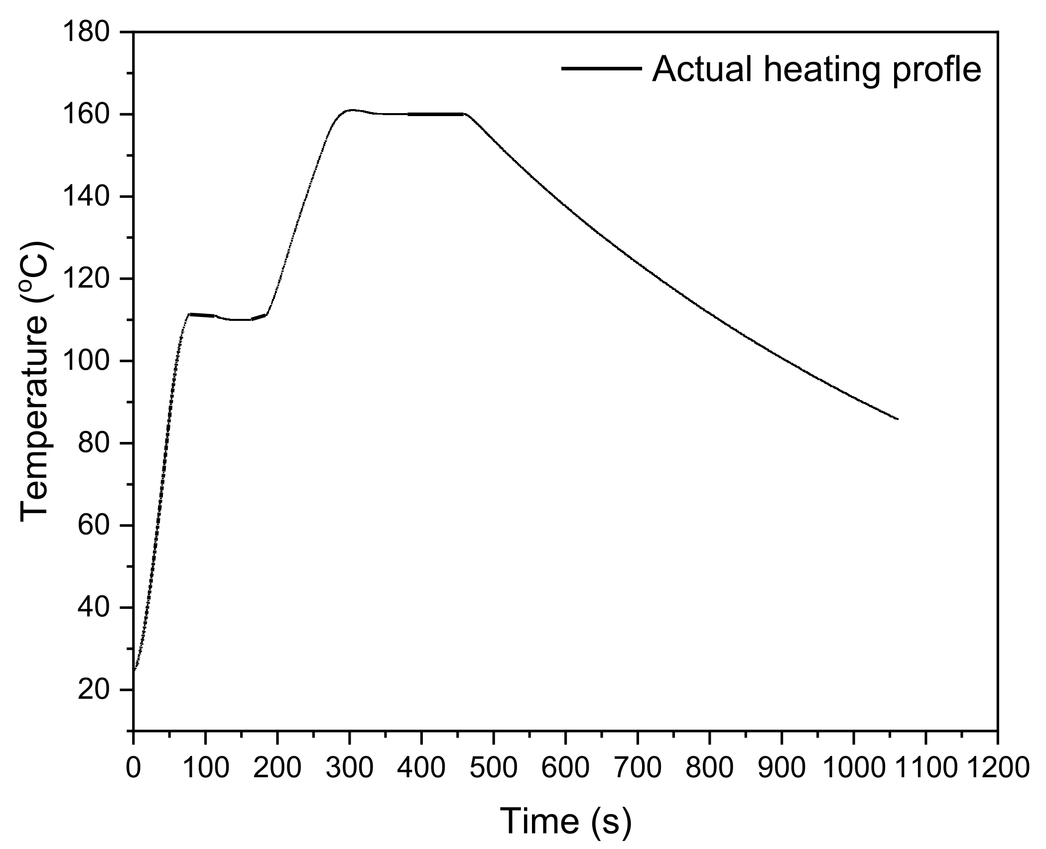
Commercial eutectic In-48Sn alloy and 2.0 or 8.0 wt.% Cu (99.9%, Nilaco Corporation, Tokyo, Japan) were melted in an electric furnace (HPM-ON, AS ONE, Osaka, Japan) under N2 atmosphere at 700 °C for 5 h. The molten metal was then poured into a steel mold and cooled naturally in air (20 °C) to form bars of a new In-Sn-Cu (ISC) alloy. The characteristics of the new ISC alloys are reported in our previous study [20], and the compositions of the alloys are shown in Table 1. The eutectic In-48Sn (IS48), In-Sn-2.0Cu (ISC482), and In-Sn-8.0Cu (ISC488) alloy bars were then rolled into 100 ± 10 μm thick foils using a rolling machine and punched into 6 mm-diameter alloy disks. Oxygen-free copper disks with diameters of 5 and 10 mm were used as upper and bottom substrates, respectively. Before making the joints, the copper disks were polished with #2000 SiC grit paper and a 1.0 µm diamond paste (DP-spray P, Struers, Cleveland, OH, USA). Subsequently, the alloy foils and the copper disks were cleaned with HCl (4 vol.%) and ethanol. Both sides of the alloy foils were coated with a drop of flux (IEC60068-69, SMIC, Tokyo, Japan), and the alloy foils were placed between the two copper disks to make the joint samples. The samples were then placed in a furnace (SK-5000 SMT-Scope, Sanyoseiko, Yamanashi, Japan) with a heating profile as shown in Figure 1. The joints were preheated at 110 °C for 60 s and reflowed at 160 °C for 90 s in N2 atmosphere; the concentration of oxygen in the furnace was maintained below 1000 ppm.

Table 1.
Chemical compositions of the IS48, ISC482, ISC488 alloys, and Cu substrate.

Figure 1.
Heating profile of the reflow process.
2.2. Characterization
A color 3D laser scanning microscope (VK-9700, Keyence, Osaka, Japan) was used to measure the contact angles of the alloys on the Cu substrate. The shear strength of the joint was determined at room temperature (20 °C) using a shear test machine (STR-1000, Rhesca, Tokyo, Japan) operated at a crosshead rate of 1 mm/min; the shear strength was calculated by dividing the maximum shear force at the failure site by the area of the alloy joint, and the average shear strength was calculated on 15 shear test results for each alloy joint. To identify the IMC at the interfacial layer between the alloy and the Cu substrate, firstly the shear-fractured samples were sectioned, mounted, ground with SiC grit papers (#150, 400, 800, 1200, and 2000), and finely polished using a 1.0 µm alumina suspension (Buehler, IL, USA). Then, the chemical composition of the IMC layers obtained using point analysis function of a field-emission electron probe microanalyzer (FE-EPMA; JXA-8530F JEOL, Tokyo, Japan). After that, to identify the crystal structural of IMC layer, the top Cu disc of the shear samples, after the shear test of the Cu/IS48/Cu and the Cu/ISC488/Cu joints, was used as an XRD sample. The fracture surfaces of the XRD samples were polished using a 1.0 µm alumina suspension until the IMC layer was detected near the substrate side. Subsequently, the samples were taken for X-ray diffraction (XRD; Ultima IV, Rigaku, Tokyo, Japan) examination in the 2θ range of 25–80° at a scan rate of 1°/min. A scanning electron microscope (SEM; SU-70, Hitachi, Osaka, Japan) equipped with energy dispersive X-ray spectroscopy (EDS) was used to study the microstructure, interfacial layer of the solder joints, and top view of the shear-fractured samples. After that, SEM and EPMA were used to study the crack propagation and the elemental distributions of the solder matrix and the interfacial layer of the solder joints after the shear test. The thicknesses of the IMC layers (observed in the EPMA map of Cu) were calculated using Image J software (National Institutes of Health, Bethesda, MD, USA). We referred to the tensile test results in the previous study [20] to plot the stress–strain graph. From this graph, we calculate the elastic modulus of IS48, ISC482, and ISC488 alloys.
3. Results and Discussion
3.1. Wettability
The contact angle (θ) is typically used as a measure of wettability of an alloy on a substrate. In the equilibrium state, the relationship between the solid–liquid (γsl), solid–vapor (γsv) and liquid–vapor (γlv) interfacial tensions is defined by Young’s equation [46]:
As shown in Figure 2, the contact angles of the IS48, ISC482, and ISC488 alloys on the Cu substrate are 16, 25, and 37°, respectively; that is, the contact angle increases with increase in the Cu content. Researchers [47,48] have studied the viscosity of the element Cu in liquid Cu-In-Sn alloys and the surface tension of the same liquid alloy. Ali et al. reported that the viscosity values of liquid Cu-In-Sn alloys at 1073 K increase from approximately 0.001 Pa·s to 0.003 Pa·s when the Cu concentration increases from 20 to 80 at.%, respectively. The surface tension values of liquid Cu-In-Sn alloys at 1073 K increase from approximately 0.49 N/m to 0.53 N/m when the Cu content increases from 20 to 30 at.%, respectively. This result is due to the higher viscosity of liquid Cu (4.5560 mPa·s) than In (0.6995 mPa·s) and Sn (1.0878 mPa·s) [47]. Therefore, the addition of Cu leads to an increase in the surface tension of the ISC molten alloy (γlv), thereby reducing the value of cosθ (in Equation (1)); this explains the increase in the θ values of the ISC482 and ISC488 alloys relative to the IS48 alloy. However, the wettability of the ISC482 and ISC488 alloys with the Cu substrate is acceptable because the contact angles are lower than those of other low-melting-temperature alloys, such as In-31.6Bi-19.6Sn (θmax = 39°) [49] and 69.5Sn–30Bi-0.5Cu (θmax = 45°) [50].
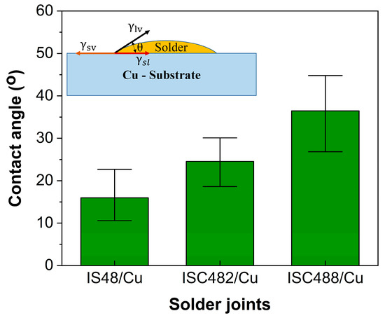
Figure 2.
Contact angles of IS48, ISC482, and ISC488 alloys on Cu substrate, and the relationship between the solid–liquid (γsl), solid–vapor (γsv) and liquid–vapor (γlv) interfacial tensions and contact angle (θ).
3.2. Microstructure Evolution
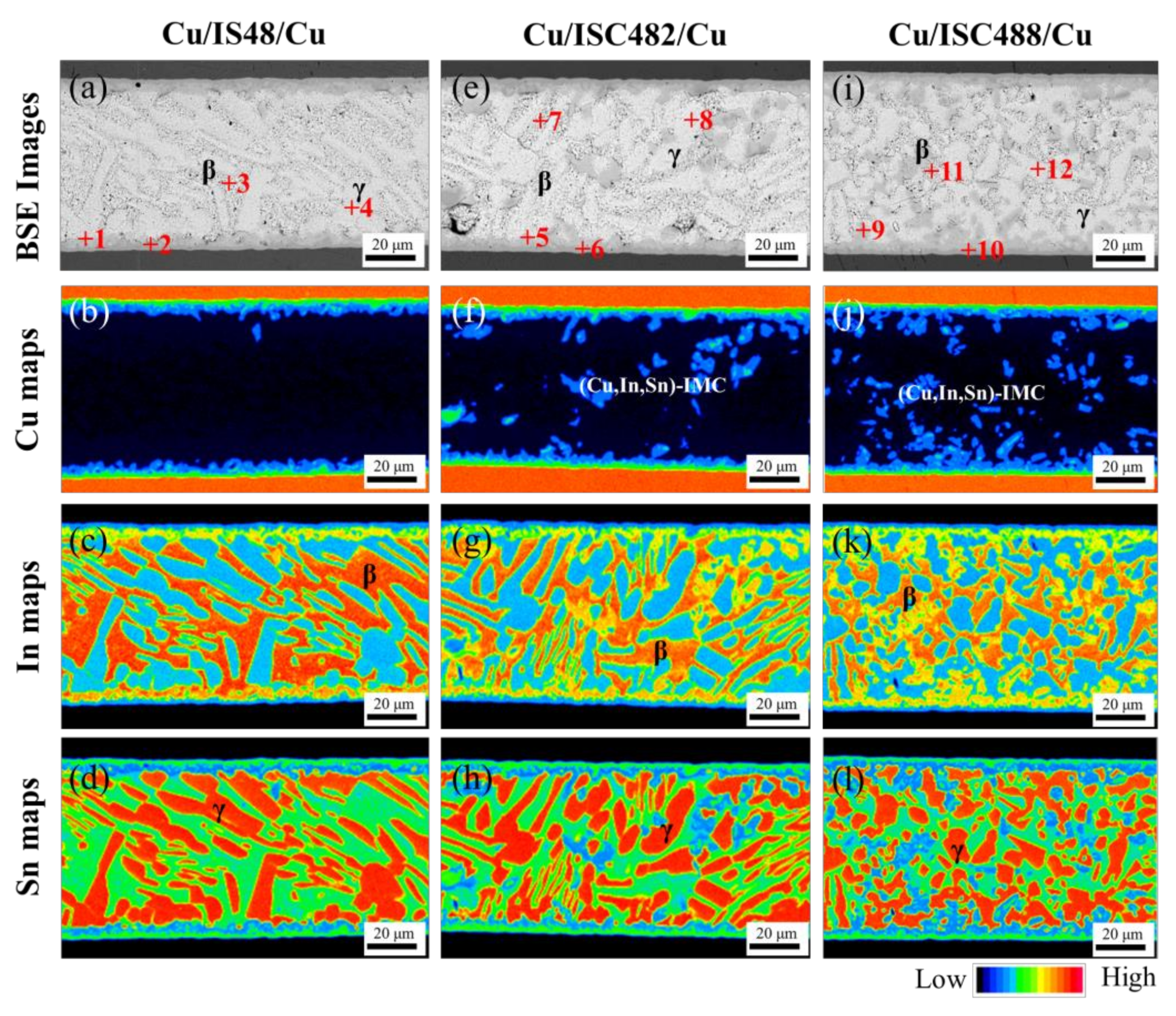
During the reflow process, the IMC layer is formed at the interface because some reactions occur between the alloys and the Cu substrate. This IMC layer plays a crucial role in the manufacture and reliability of the solder joints [51]. Figure 3 shows the high-magnification view of the cross-sectional backscattered electrons (BSE) and EPMA images of the Cu/IS48/Cu, Cu/ISC482/Cu, and Cu/ISC488/Cu alloy joints. The continuous layers of the IMCs indicate good bonding between the ISC alloys and the Cu disks (Figure 3b,f,j); this can be attributed to the good wettability of all the alloys. Two main phases, namely, β-In3Sn and γ-InSn4, are formed in the solder matrices of In-Sn-xCu/Cu joints. The β-(In,Sn) and the γ-(In,Sn) phases are formed through eutectic reactions during cooling from 115 to 113 °C, as discussed in our previous study [20]; these results are consistent with the phase constitutions in the In–Sn phase diagram [52] and other reported results [53]. The (Cu,In,Sn)-IMC formed in the ISC482 and ISC488 alloy matrices (Figure 3f–j) lead to finer microstructures compared to that of the IS48 alloy. The microstructural evolutions of the IS48, ISC482, and ISC488 alloy matrices after the reflow are consistent with the behaviors of bulk alloys after casting, as mentioned in our previous study [20]. The chemical compositions of the β-(In,Sn), γ-(In,Sn) phases and the IMC layers obtained using EPMA point analyses are summarized in Table 2. The results indicate the formation of two layers of IMCs at the interface between the ISC alloys and the Cu substrate: a Cu-rich Cu6(In,Sn)5 layer near the Cu substrate and a Cu-deficient Cu(In,Sn)2 layer near the alloy matrix.

Figure 3.
The high-magnification view of the cross-sectional BSE and EPMA images of the: (a–d) Cu/IS48/Cu joint, (e–h) Cu/ISC482/Cu joint, and (i–l) Cu/ISC488/Cu joint; and the locations (1–12) of the EPMA points listed in Table 2. Where β and γ correspond to In3Sn and InSn4 phases, respectively. The plus symbols represent the locations of the analysis points.
Table 2.
Chemical composition of the marked points in Figure 3.
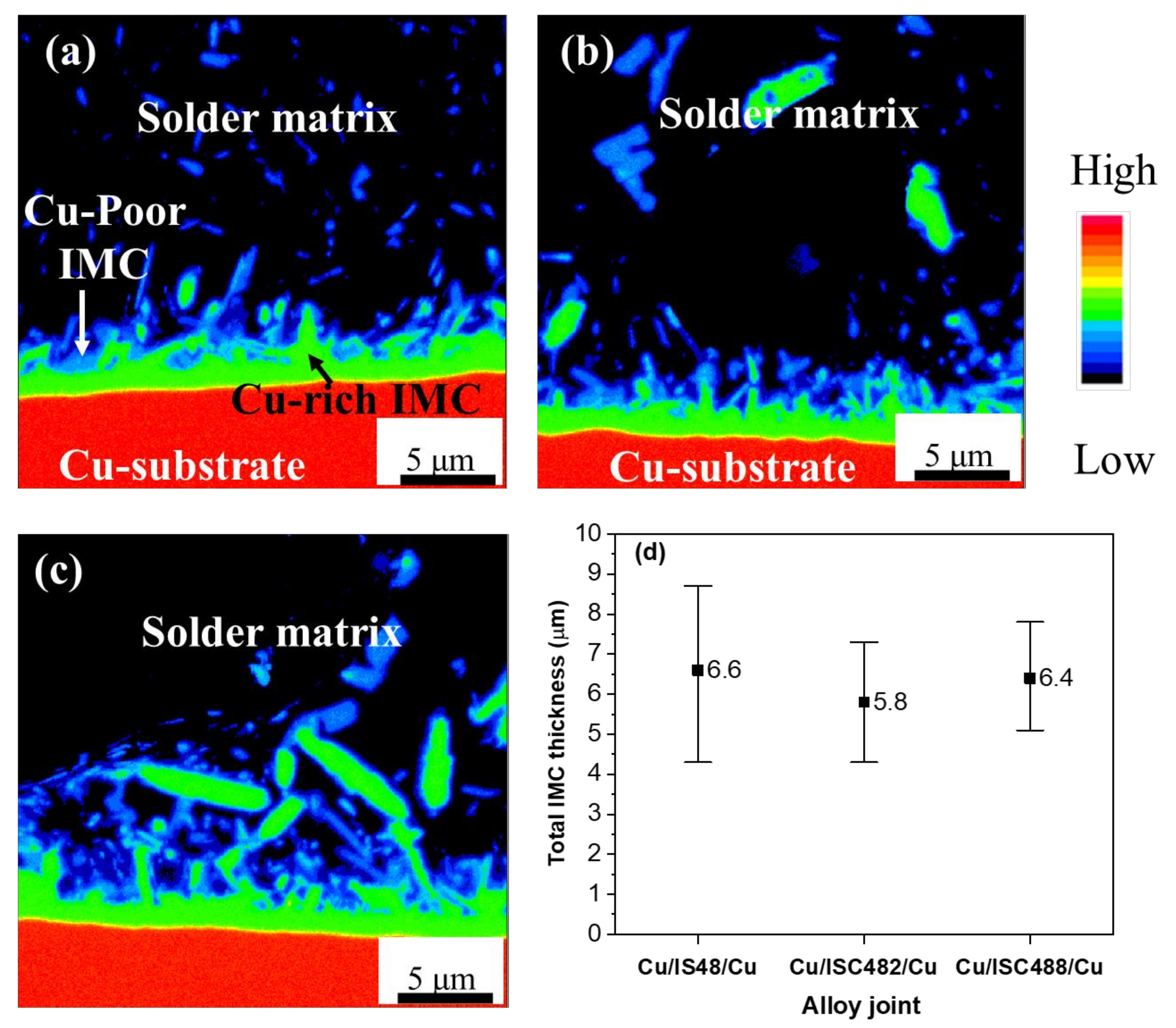
The total thicknesses of the IMC layers [Cu6(In,Sn)5 + Cu(In,Sn)2] for each interface, as calculated using the ImageJ software and high-magnification EMPA Cu maps, are shown in Figure 4. The error bars show the standard deviations within the measured values of 40 positions in the EPMA Cu maps of each alloy.
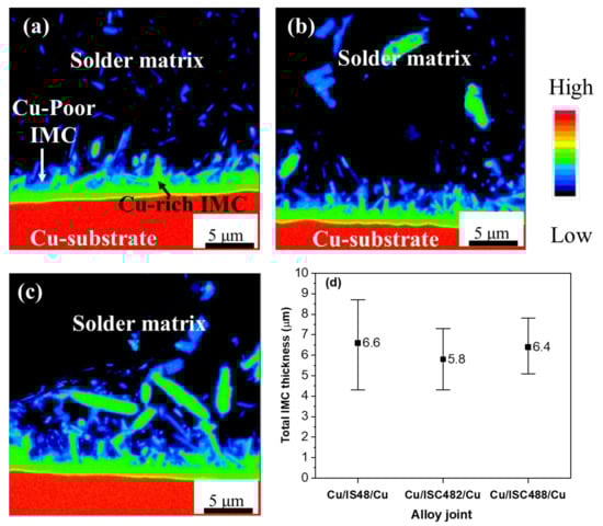
Figure 4.
(a–c) Typical EMPA Cu maps images, and (d) total thickness of the IMC layer in Cu/IS48/Cu, Cu/ISC482/Cu, and Cu/ISC488/Cu joints.
The total thickness of the IMC layer of IS48 is the highest, approximately 6.6 μm, followed by that of ISC488 (6.4 μm) and ISC482 (5.8 μm) (Figure 4d). The reduction in the thickness of the IMC layer at the interface between the ISC alloys and the Cu substrate when compared to that of the IS48 alloy can be attributed to the presence of Cu in the ISC alloy; it suppresses the diffusion of Cu from the substrate to the molten In–Sn alloy. During the reflow process, the Cu atoms from the substrate tend to diffuse into the liquid In–Sn alloy. Therefore, the Cu distributed in the Cu-free IS48 alloy matrix is detected after the reflow process (Figure 4a). At the early stage of soldering reactions, the Cu6(In,Sn)5 IMC is the dominant phase during the liquid/solid In-Sn(l)/Cu(s) reactions, which is consistent with the η-Cu6Sn5 phase formed during Sn/Cu interfacial reaction [18]. Subsequently, the Cu-deficient Cu(In,Sn)2 IMC is formed during the cooling process through solid–solid transformation from the Cu-rich IMC [20,37]. Furthermore, at the interface between the ISC alloys and the Cu substrate, a barrier layer of Cu-rich Cu6(In,Sn)5 IMC is quickly formed owing to the presence of 2 wt.% Cu in the ISC482 and 8 wt.% Cu in the ISC488 alloys, which prevents the diffusion of Cu from the substrate into the molten alloy [54]. Although the large amount of Cu in the ISC488 alloy leads to low amount of diffused Cu from the substrate into the liquid alloy, the higher amount of (Cu, In, Sn)-IMC present in the ISC488 alloy matrix near the interface tends to merge with the Cu(In,Sn)2 layer of the ISC488/Cu interfacial layer. Consequently, the ISC488/Cu interface exhibits higher total thickness and surface roughness compared to the ISC482/Cu interface (Figure 4d).
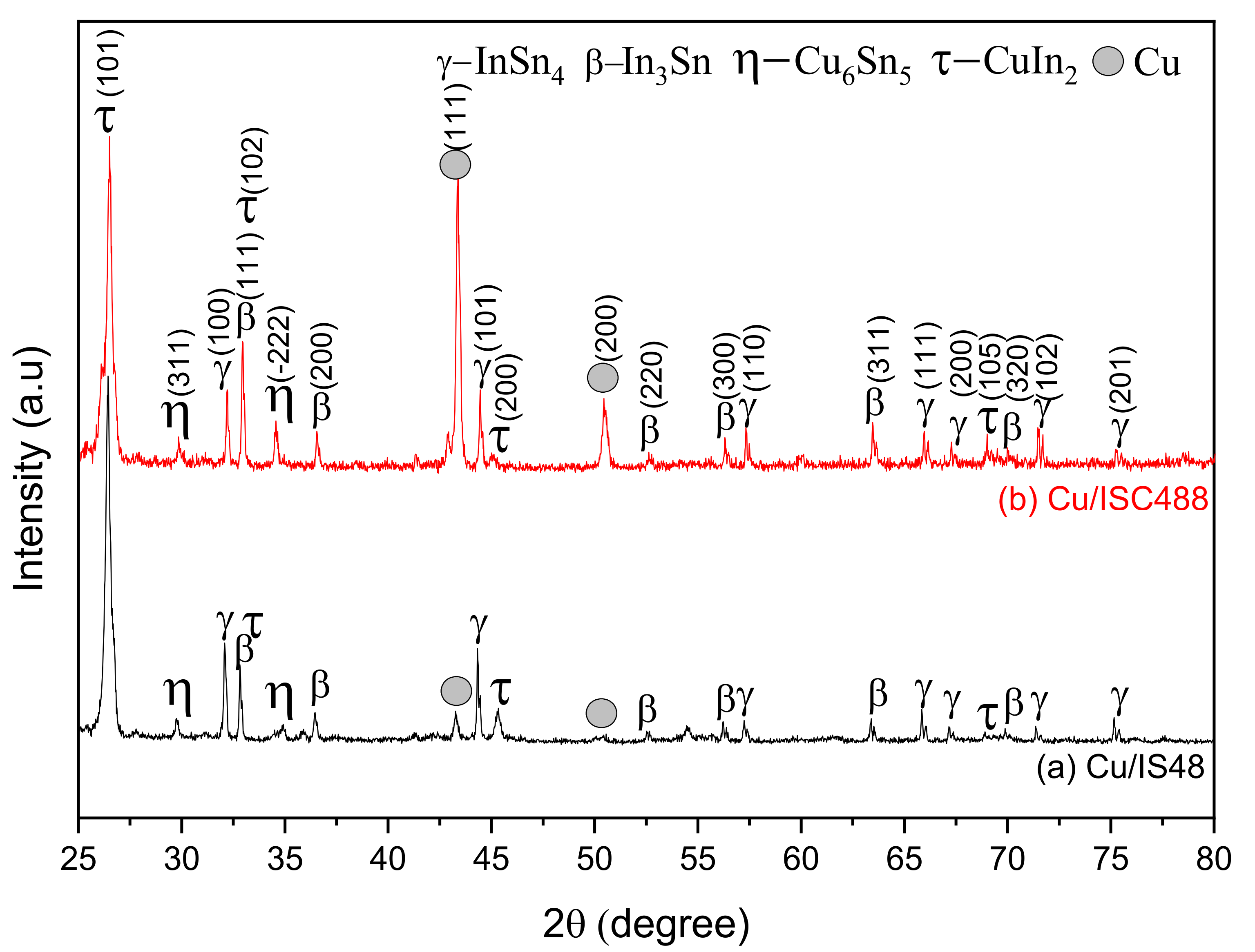
Figure 5 shows the XRD patterns of IS48/Cu and ISC488/Cu interfaces; the peaks at 2θ angles of 33.15, 36.85, 53.15, 56.40, 63.75 and 69.55° correspond to β-In3Sn (PDF card # 00-007-0345) and the peaks at 2θ angles of 32.35, 44.75, 57.40, 66.10, 67.38, 71.75 and 75.50° correspond to γ-InSn4 (PDF card # 00-007-0396) because the solder remained on the polished samples of IS48/Cu and ISC488/Cu interfaces, these peaks are consistent with the XRD result of IS48 and IS488 alloys as we reported in our previous study [20]. The peaks at 2θ angles of 43.45 and 50.31° originate from the Cu substrate (PDF card # 00-001-1241). The peaks at 29.98, and 34.19° correspond to η-Cu6Sn5 (PDF card # 01-076-2703). It is noted that Cu6(In,Sn)5 has a Cu6Sn5 crystal structure owing to the dissolution of In atoms in the Cu6Sn5 crystal lattice to form Cu6(In,Sn)5 IMC layer at the solder/Cu interface [55]. Moreover, the peaks at 26.24, 45.41, 33.43, and 68.93° correspond to τ-CuIn2 (PDF card # 01-080-3063). As Sn and In atoms have similar atomic radii, Sn atoms can substitute In atoms through solid-state diffusion during cooling after the reflow process [56,57]; hence, the IMC near the solder matrix should be represented as Cu(In,Sn)2 [57]. It can be noted that the XRD results are consistent with the estimated IMC from the EPMA results as mentioned in Table 2.
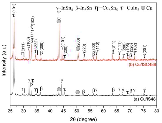
Figure 5.
XRD patterns of the (a) IS48/Cu and (b) ISC488/Cu alloys.
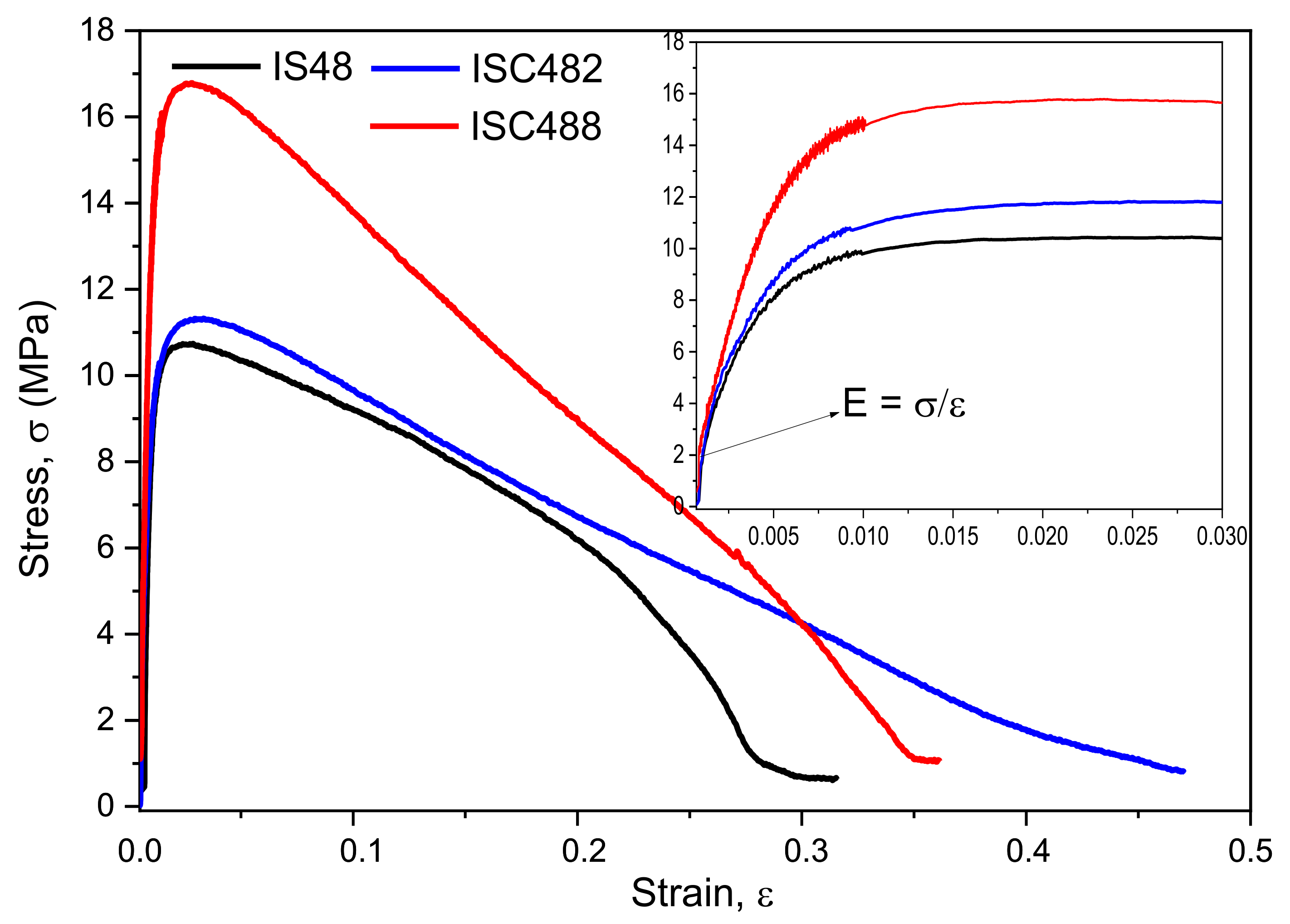
3.3. Elastic Modulus of Alloys
In our previous study [20], the average tensile strength of IS48, ISC482, and ISC488 are 10.8, 11.2, and 16.8 MPa, respectively. Figure 6 shows typical engineering stress–strain curves of IS48, ISC482, and ISC488 alloys, which consist of an elastic region and a plastic region. In the elastic region, the engineering stress is linear, with the engineering strain conforming to Hooke’s law as follows [58]:
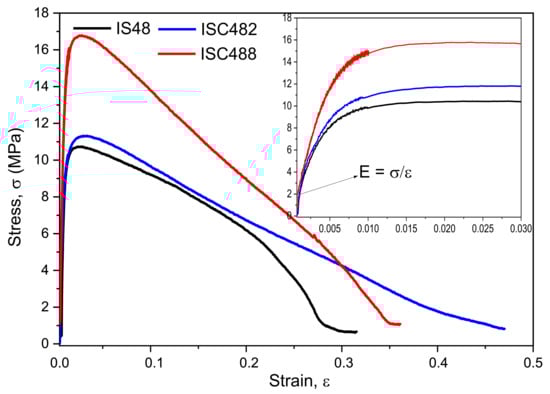
Figure 6.
Typical stress–strain curves of IS48, ISC482 and ISC488 alloys.
Here, E is the elastic modulus, which can be determined from the slope of the elastic portion of the stress–strain curve, σ is the engineering stress, and ε is the engineering strain. We calculated that the elastic modulus of IS48, ISC482 and ISC488 alloys are 24.1, 25.1, and 26.9 GPa, respectively. The elastic modulus of IS48 is in agreement with the value reported by Kim [59]. All alloys exhibit a low elastic modulus compared to that of commercial SAC305 alloy (54.0 GPa) [36] and Sn-58Bi alloy (41.3 GPa) [60]. This is an advantage of IS48, ISC482, and ISC488 alloys to be able to apply in flexible electronic devices. Moreover, the tensile strength of ISC alloys increases with the increase in Cu content, which is expected that Cu addition can help improve the creep resistance and thermal failure resistance of the ISC alloys.
3.4. Shear Strength and Fracture Behavior of Solder Joint
The fine microstructures of the ISC482 and ISC488 alloy matrices and the thickness and roughness of the IMC layer significantly affect the alloy/Cu joint reliability. Figure 7 shows the shear strengths of Cu/IS48/Cu, Cu/ISC482/Cu, and Cu/ISC488/Cu joints; the error bar displays the standard deviations within 15 test results for each solder joint. The Cu/IS48/Cu joint exhibited an average shear strength of approximately 14.5 MPa, which is nearly equal to that of the Cu/ISC488/Cu joint (14.3 MPa) and approximately 14% lower than that of the Cu/ISC482/Cu joint (16.5 MPa).
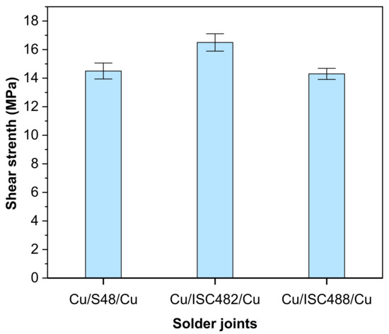
Figure 7.
Shear strengths of the alloy joints.
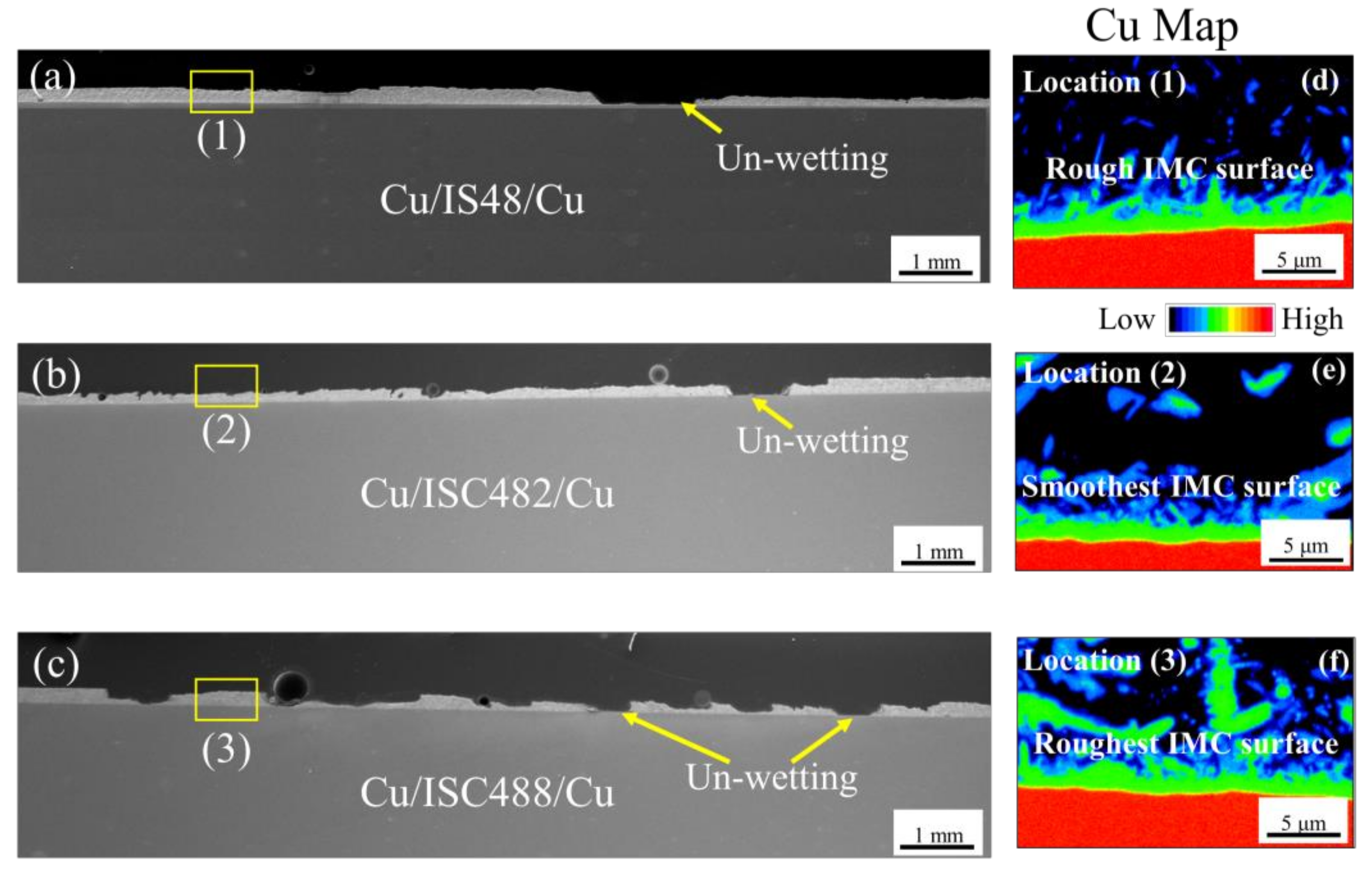
Figure 8a–c shows the SEM images of typical cross-sectional fractured samples. Crack propagation occurs in the alloy matrices of both the ISC alloy joints and along the alloy/IMC interfaces with formation of few non-wetting regions between the alloys and the substrates owing to the outgassing phenomenon during the reflow process Figure. 8d–f shows the EPMA maps of Cu obtained from locations (1), (2), and (3) marked in Figure 8a–c, respectively. The ISC482/Cu interface has a smoother IMC surface than the IS48/Cu interface, while the ISC488/Cu interface exhibits the roughest IMC surface among all the alloy/Cu interfaces. These results are consistent with those of Figure 4; the IS48/Cu interface showed the highest total thickness of IMC layer owing to the absence of Cu in the alloy matrix, and the IS482/Cu interface showed a lower total thickness of IMC layer and a highly smooth surface owing to the presence of 2 wt.% Cu in the alloy matrix [61]. It can be noted that the thickness and morphology of the intermetallic layer may be one of the factors affecting the shear strength of the solder joints. Another factor that cannot be ignored also has a significant influence on the shear strength—the void defect in the joint [62].

Figure 8.
SEM images of typical cross-sectional fractured samples of (a) Cu/IS48/Cu, (b) Cu/ISC482/Cu, and (c) Cu/ISC488/Cu joints. (d–f) EPMA Cu map images of typical locations (1, 2, and 3) at the interface of the fractured samples.
Figure 9 shows top view SEM images of the fractured samples of the Cu/IS48/Cu, Cu/ISC482/Cu, and Cu/ISC488/Cu joints at the bottom disk side after shear testing. Figure 9b,c show that the void distribution in the shear fracture surfaces of ISC482/Cu and ISC488/Cu increases with an increase in the Cu content, and is higher than that of IS48/Cu. This phenomenon can be attributed to the high viscosity of Cu leading to an increase in surface tension of ISC alloys in the liquid state as mentioned in the previous section. The percentage of voids and non-wetting areas on the shear fracture surface samples was measured using ImageJ software. Four SEM images of the fractured samples for each alloy joint were used for this measurement; the smallest area was calculated as 0.01 mm2, and the results are summarized in Figure 10. The results indicate that the percentage of non-wetting (3.5%) and voids (15.7%) are largest on the fracture surfaces of ISC488/Cu because ISC488/Cu exhibits the lowest wettability on the Cu substrate, as discussed previously. The next largest values are for the Cu/ISC482/Cu joint (2.5% and 8.2%, respectively), and Cu/ISC482/Cu joint (0.97% and 7.3%, respectively). As a result, the void defect [62] and non-wetting regions may be the main reasons for the reduced shear strength of Cu/ISC488/Cu joints.
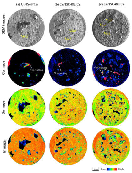
Figure 9.
Top view SEM images of the fractured samples at the bottom disks after the shear test: (a) Cu/IS48, (b) Cu/ISC482, and (c) Cu/ISC488.
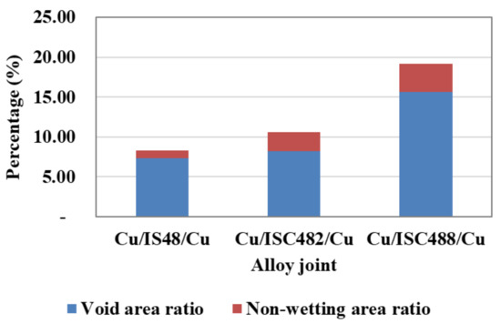
Figure 10.
Percentage of void and non-wetting area on fracture surface of alloy joints.
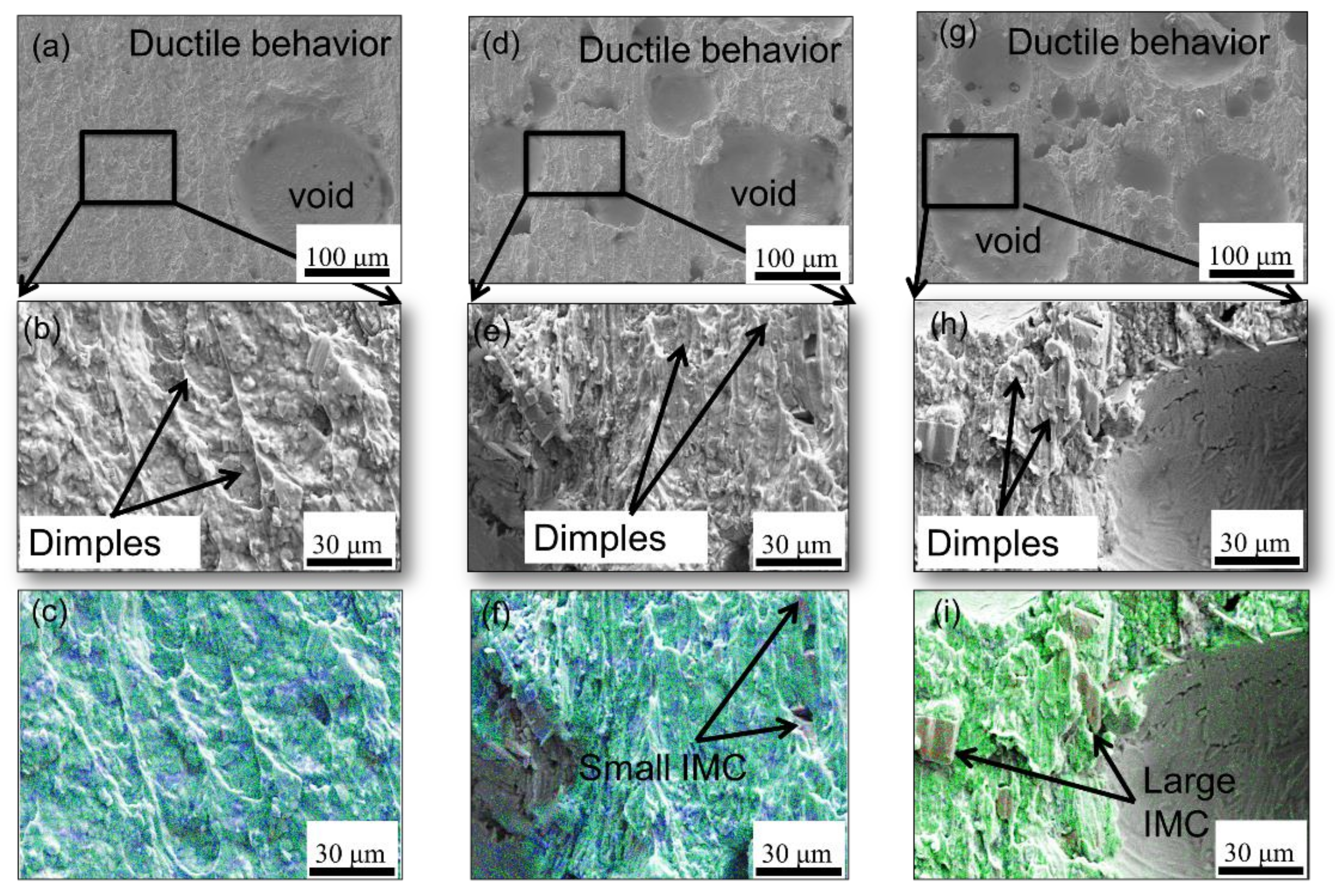
Figure 11 shows that although all the alloy joints exhibit ductile behavior with many dimples on the fracture surface, the fractured surface of IS48/Cu has fewer voids and no IMC. Few large fragments of (Cu, In, Sn)-IMC are observed near the voids on the fractured surface of ISC488/Cu (Figure 11i), which indicates stress concentration of voids. This confirms the low shear strength of the ISC488/Cu joint. Conversely, few small fragments of (Cu, In, Sn)-IMC are found on the fractured surface of ISC482/Cu (Figure 11f), and the number and size of the voids are smaller when compared to those observed on the fractured surface of ISC488/Cu. Hence, the ISC482/Cu joint exhibited higher shear strength compared to the other alloy joints.

Figure 11.
SEM images of the fracture surface of shear test samples: (a–c) Cu/IS48/Cu, (d–f) Cu/ISC482/Cu, and (g–i) Cu/ISC488/Cu joints.
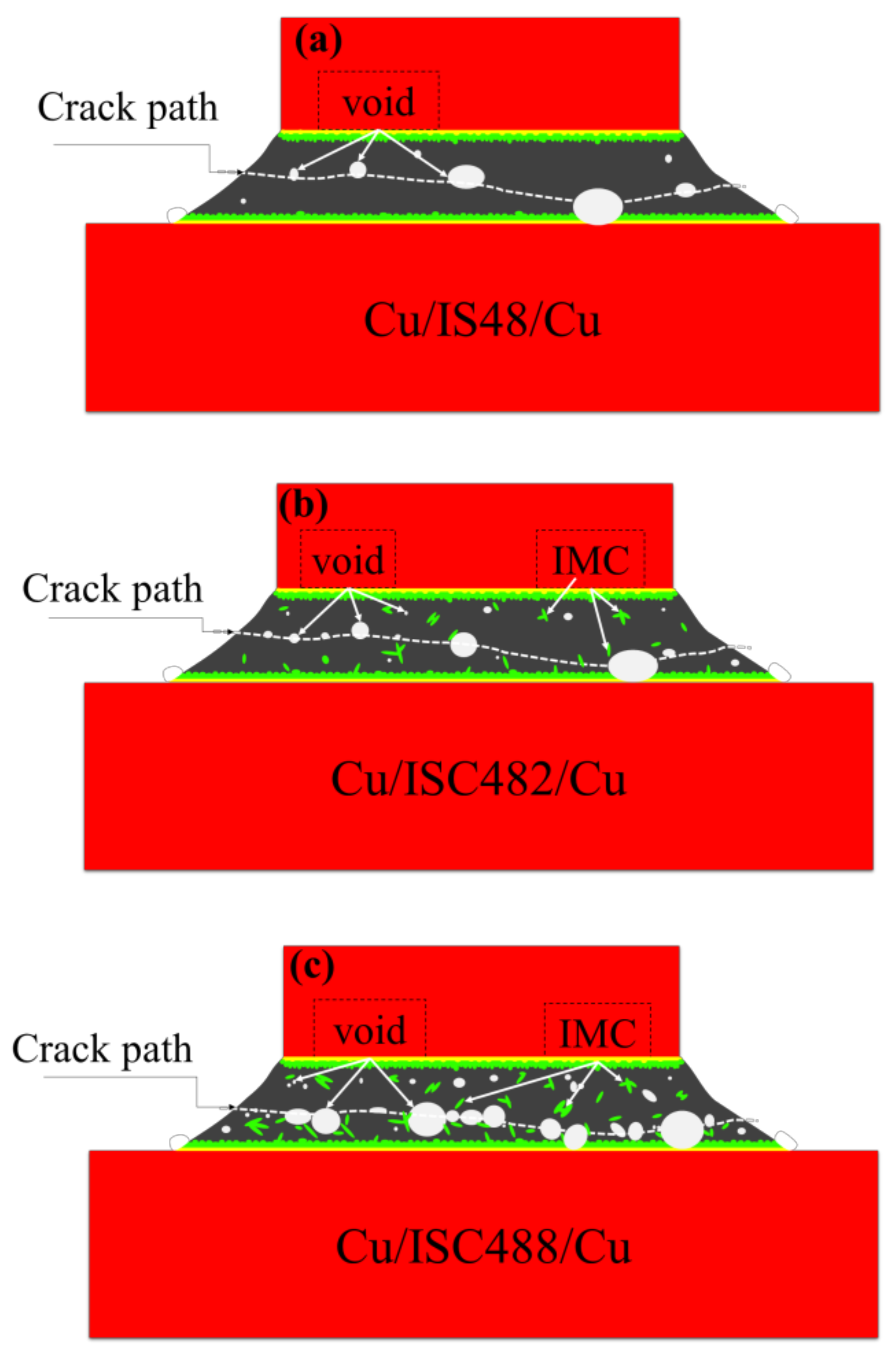
It has been reported that the tensile strength of bulk materials such as low carbon steel and stainless steel [63] or irradiated materials [64] has linear relationships with shear strength. As previous discussion, crack propagation occurs in the alloy matrices of all alloy joints; therefore, the strength of the alloy matrices should be the main determinant of the shear strength of the joints. It means that there should be a certain relationship between the shear strength of the joint and the tensile strength of the alloy. We calculated that the shear strength of Cu/IS48 and Cu/ISC482 joints is approximately 1.34 and 1.47 times the tensile strength of alloy IS48 and alloy ISC482, respectively. While the shear strength of the Cu/ISC488 joint is approximately 0.85 times the tensile strength of ISC488 alloy. It is well known that the shear strength of solder joints is adversely affected by the intermetallic layer and the percentage of void defects in the joint [62,65,66]. Therefore, although ISC488 alloy has the highest tensile strength among the alloys studied, the highest percentage of void in the joint leads to a decrease in shear strength of Cu/ISC488/Cu joint. Due to many factors affecting the strength of the joint, from the tensile test results of the three alloys and the shear test results of the three corresponding joints in this study, we did not find a general relationship between the shear strength of the joint and the tensile strength of the alloy. Figure 12 shows the schematic of the crack propagation and void distribution in Cu/IS48/Cu, Cu/ISC482/Cu, and Cu/ISC488/Cu alloy joints. The fine microstructure with a small amount of (Cu, In, Sn)-IMC in the ISC482 alloy matrix (Figure 3e–g and Figure 12b) and the thin interfacial IMC layer enhance the reliability of the Cu/ISC482/Cu joint. Large β and γ grains (Figure 3a–d) and the absence of (Cu, In, Sn)-IMC layer in the IS48 alloy matrix (Figure 12a) [20] result in lower shear strength of the Cu/IS48/Cu joint compared to that of the Cu/ISC482/Cu joint. The Cu/ISC488/Cu joint exhibits finer grains (Figure 3i–l); however, it also shows the highest number of voids (Figure 10 and Figure 12c) and the roughest interfacial IMC layer among all the alloy joints (Figure 8f). These act as additional stress concentration points [67] causing a reduction in the shear strength of the Cu/ISC488/Cu joint, as shown in Figure 7.
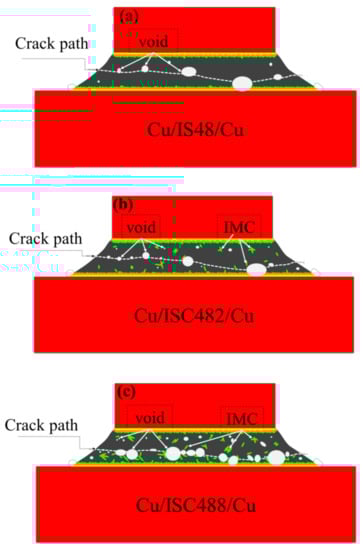
Figure 12.
Schematics of crack propagation and void distribution in (a) Cu/IS48/Cu, (b) Cu/ISC482/Cu, and (c) Cu/ISC488/Cu joints.
4. Conclusions
The effects of 2.0 and 8.0 wt.% Cu addition on the wettability, microstructure evolution, and shear strength of In-Sn-xCu/Cu joints were analyzed and compared with that of In-48Sn/Cu joint. The addition of Cu increased the contact angle of the In-Sn-xCu alloys on the Cu substrate owing to the higher viscosity of liquid Cu than that of In and Sn. All ISC alloys exhibited acceptable wettability, as indicated by the formation of continuous Cu6(In,Sn)5 + Cu(In,Sn)2 IMC layer at the In-Sn-xCu/Cu interface. Both Cu/IS482/Cu and Cu/ISC488/Cu joints exhibited a comparable and better shear strength than Cu/IS48/Cu joint, and all alloys have a low elastic modulus. As a result, the new ISC482 and ISC488 alloys are good candidates to replace IS48 alloy in flexible electronic applications, where low-temperature solder is required. Further studies on joint reliability, creep resistance and fatigue failure resistance of alloy will provide a complete overview of ISC482 and ISC488 alloys.
Author Contributions
Conceptualization, D.L.H. and H.N.; Methodology, D.L.H.; Investigation, D.L.H.; Writing—original draft preparation, D.L.H.; Writing—review and editing, H.N., Y.-A.S. and F.H.; Supervision, H.N.; All authors have read and agreed to the published version of the manuscript.
Funding
This research was funded by the Ministry of Education, Culture, Sports, Science and Technology in Project to Create Research and Education Hubs for Innovative Manufacturing in Asia, Osaka University of Special Budget Project.
Data Availability Statement
Not applicable.
Acknowledgments
Duy Le Han would like to thank the Monbukagakusho (MEXT) scholarship. Hiroshi Nishikawa would like to thank the Ministry of Education, Culture, Sports, Science and Technology in Project to Create Research and Education Hubs for Innovative Manufacturing in Asia, Osaka University of Special Budget Project for the financial support during this study.
Conflicts of Interest
The authors declare no conflict of interest regarding the publication of this article.
References
- Zardetto, V.; Brown, T.M.; Reale, A.; Di Carlo, A. Substrates for flexible electronics: A practical investigation on the electrical, film flexibility, optical, temperature, and solvent resistance properties. J. Polym. Sci. Part B Polym. Phys. 2011, 49, 638–648. [Google Scholar] [CrossRef]
- Khan, Y.; Thielens, A.; Muin, S.; Ting, J.; Baumbauer, C.; Arias, A.C. A New Frontier of Printed Electronics: Flexible Hybrid Electronics. Adv. Mater. 2019, 32, 1–29. [Google Scholar] [CrossRef]
- Corzo, D.; Tostado-Blázquez, G.; Baran, D. Flexible Electronics: Status, Challenges and Opportunities. Front. Electron. 2020, 1, 1–13. [Google Scholar] [CrossRef]
- Wang, P.; Hu, M.; Wang, H.; Chen, Z.; Feng, Y.; Wang, J.; Ling, W.; Huang, Y. The Evolution of Flexible Electronics: From Nature, Beyond Nature, and To Nature. Adv. Sci. 2020, 7, 1–29. [Google Scholar] [CrossRef] [PubMed]
- Zhang, P.; Xue, S.; Wang, J. New challenges of miniaturization of electronic devices: Electromigration and thermomigration in lead-free solder joints. Mater. Des. 2020, 192, 108726. [Google Scholar] [CrossRef]
- Abtew, M.; Selvaduray, G. Lead-free solders in microelectronics. Mater. Sci. Eng. R Rep. 2000, 27, 95–141. [Google Scholar] [CrossRef]
- Jiang, N.; Zhang, L.; Liu, Z.Q.; Sun, L.; Long, W.M.; He, P.; Xiong, M.Y.; Zhao, M. Reliability issues of lead-free solder joints in electronic devices. Sci. Technol. Adv. Mater. 2019, 20, 876–901. [Google Scholar] [CrossRef] [PubMed] [Green Version]
- Jeong, G.; Yu, D.-Y.; Baek, S.; Bang, J.; Lee, T.-I.; Jung, S.-B.; Kim, J.; Ko, Y.-H. Interfacial Reactions and Mechanical Properties of Sn–58Bi Solder Joints with Ag Nanoparticles Prepared Using Ultra-Fast Laser Bonding. Materials 2021, 14, 335. [Google Scholar] [CrossRef]
- Lee, C.-J.; Min, K.D.; Park, H.J.; Jung, S.-B. Mechanical properties of Sn-58 wt%Bi solder containing Ag-decorated MWCNT with thermal aging tests. J. Alloy. Compd. 2019, 820, 153077. [Google Scholar] [CrossRef]
- Le Han, D.; Shen, Y.-A.; Jin, S.; Nishikawa, H. Microstructure and mechanical properties of the In–48Sn–xAg low-temperature alloy. J. Mater. Sci. 2020, 55, 10824–10832. [Google Scholar] [CrossRef]
- Spinella, L.; Bosco, N. Thermomechanical fatigue resistance of low temperature solder for multiwire interconnects in photovoltaic modules. Sol. Energy Mater. Sol. Cells 2021, 225, 111054. [Google Scholar] [CrossRef]
- Jiang, N.; Zhang, L.; Gao, L.-L.; Song, X.-G.; He, P. Recent advances on SnBi low-temperature solder for electronic interconnections. J. Mater. Sci. Mater. Electron. 2021, 32, 22731–22759. [Google Scholar] [CrossRef]
- Shen, Y.-A.; Zhou, S.; Li, J.; Yang, C.; Huang, S.; Lin, S.; Nishikawa, H. Sn-3.0Ag-0.5Cu/Sn-58Bi composite solder joint assembled using a low-temperature reflow process for PoP technology. Mater. Des. 2019, 183, 108144. [Google Scholar] [CrossRef]
- Shen, Y.-A.; Chen, S.-W.; Chen, H.-Z.; Chang, C.-M.; Ouyang, Y.-H. Extremely thin interlayer of multi-element intermetallic compound between Sn-based solders and FeCoNiMn high-entropy alloy. Appl. Surf. Sci. 2021, 558, 149945. [Google Scholar] [CrossRef]
- Davila-Frias, A.; Yadav, O.P.; Marinov, V. A Review of Methods for the Reliability Testing of Flexible Hybrid Electronics. IEEE Trans. Compon. Packag. Manuf. Technol. 2020, 10, 1902–1912. [Google Scholar] [CrossRef]
- Kim, D.-G.; Jung, S.-B. Interfacial reactions and growth kinetics for intermetallic compound layer between In–48Sn solder and bare Cu substrate. J. Alloy. Compd. 2005, 386, 151–156. [Google Scholar] [CrossRef]
- Goldstein, J.L.F.; Morris, J.W. The Effect of Substrate on the Microstructure and Mechanical Behavior of Eutectic Indium-Tin. MRS Proc. 1993, 323, 159. [Google Scholar] [CrossRef]
- Chuang, T.H.; Yu, C.L.; Chang, S.Y.; Wang, S.S. Phase identification and growth kinetics of the intermetallic compounds formed during In-49Sn/Cu soldering reactions. J. Electron. Mater. 2002, 31, 640–645. [Google Scholar] [CrossRef]
- Koo, J.-M.; Jung, S.-B. Reliability of in-48Sn solder/Au/Ni/Cu BGA packages during reflow process. J. Electron. Mater. 2005, 34, 1565–1572. [Google Scholar] [CrossRef]
- Le Han, D.; Shen, Y.-A.; He, S.; Nishikawa, H. Effect of Cu addition on the microstructure and mechanical properties of In–Sn-based low-temperature alloy. Mater. Sci. Eng. A 2021, 804, 140785. [Google Scholar] [CrossRef]
- Choi, K.; Lee, H.; Bae, H.; Eom, Y.; Lee, J.H. Interconnection Technology Based on InSn Solder for Flexible Display Applications. ETRI J. 2015, 37, 387–394. [Google Scholar] [CrossRef]
- Evans, J.W. A Guide to Lead-free Solders—Physical Metallurgy and Reliability; Engelmaier, W., Ed.; Springer: London, UK, 2007; ISBN 9781846283093. [Google Scholar]
- Long, X.; Tang, W.; Xu, M.; Keer, L.M.; Yao, Y. Electric current-assisted creep behaviour of Sn–3.0Ag–0.5Cu solder. J. Mater. Sci. 2018, 53, 6219–6229. [Google Scholar] [CrossRef]
- Wang, W.; Chen, Z.; Wang, S.; Long, X. Mechanics-based acceleration for estimating thermal fatigue life of electronic packaging structure. Microelectron. Reliab. 2020, 107, 113616. [Google Scholar] [CrossRef]
- Long, X.; Liu, Y.; Jia, F.; Wu, Y.; Fu, Y.; Zhou, C. Thermal fatigue life of Sn–3.0Ag–0.5Cu solder joint under temperature cycling coupled with electric current. J. Mater. Sci. Mater. Electron. 2019, 30, 7654–7664. [Google Scholar] [CrossRef]
- Seyyedi, J. Thermal Fatigue Behaviour of Low Melting Point Solder Joints. Solder. Surf. Mt. Technol. 1993, 5, 26–32. [Google Scholar] [CrossRef]
- Wang, J.; Mao, D.; Shi, L.; Zhang, W.; Zhang, X. Effect of Zinc Addition on the Microstructure, Thermal and Mechanical Properties of Indium-Tin-xZinc Alloys. J. Electron. Mater. 2019, 48, 817–826. [Google Scholar] [CrossRef]
- Kim, S.H.; Yeon, S.-M.; Kim, J.H.; Park, S.J.; Lee, J.E.; Park, S.-H.; Choi, J.-P.; Aranas, C.J.; Son, Y. Fine Microstructured In–Sn–Bi Solder for Adhesion on a Flexible PET Substrate: Its Effect on Superplasticity and Toughness. ACS Appl. Mater. Interfaces 2019, 11, 17090–17099. [Google Scholar] [CrossRef] [PubMed]
- Das, S.; Sharif, A.; Chan, Y.; Wong, N.; Yung, W.K.C. Influence of small amount of Al and Cu on the microstructure, microhardness and tensile properties of Sn–9Zn binary eutectic solder alloy. J. Alloy. Compd. 2009, 481, 167–172. [Google Scholar] [CrossRef]
- Qiu, J.; Peng, Y.; Gao, P.; Li, C. Effect of Cu Content on Performance of Sn-Zn-Cu Lead-Free Solder Alloys Designed by Cluster-Plus-Glue-Atom Model. Materials 2021, 14, 2335. [Google Scholar] [CrossRef]
- Shen, J.; Pu, Y.; Yin, H.; Luo, D.; Chen, J. Effects of minor Cu and Zn additions on the thermal, microstructure and tensile properties of Sn-Bi-based solder alloys. J. Alloys Compd. 2014, 614, 63–70. [Google Scholar] [CrossRef]
- Said, R.M.; Salleh, M.A.A.M.; Amran, N.A.A.; Ramli, M.I.I. Microstructure Evolution of Sn-Cu Based Solder Paste with Different Cu Concentration Subjected to Multiple Reflows. Solid State Phenom. 2018, 280, 206–211. [Google Scholar] [CrossRef]
- Mehreen, S.U.; Nogita, K.; McDonald, S.; StJohn, D. Effect of Zn addition on Cu3Sn formation in Sn-10Cu alloys. IOP Conf. Series: Mater. Sci. Eng. 2019, 701, 012009. [Google Scholar] [CrossRef]
- Cho, J.; Mallampati, S.; Schoeller, H.; Yin, L.; Shaddock, D. Developments of Bi-Sb-Cu alloys as a high-temperature Pb-free solder. In Proceedings of the 2015 IEEE 65th Electronic Components and Technology Conference (ECTC), San Diego, CA, USA, 26–29 May 2015; 2015; pp. 1251–1256. [Google Scholar] [CrossRef]
- Tumminello, S.; Del Negro, N.; Carrascal, C.; Fries, S.G.; Alonso, P.R.; Sommadossi, S. Multiphase Characterization of Cu-In-Sn Alloys with 17 at.% Cu and Comparison with Calculated Phase Equilibria. J. Phase Equilibria Diffus. 2017, 38, 276–287. [Google Scholar] [CrossRef]
- Yang, L.; Yang, Y.; Zhang, Y.; Xu, F.; Qiao, J.; Lu, W.; Yu, B. Microstructure evolution and mechanical properties of the In–Sn–20Cu composite particles TLP bonding solder joints. Appl. Phys. A 2020, 126, 1–8. [Google Scholar] [CrossRef]
- Susan, D.F.; Rejent, J.A.; Grant, R.P.; Vianco, P.T. The Solidification Behavior and Microstructure of In-Sn-Cu Solder Alloys with Low Cu. In Proceedings of the 4th International Brazing and Soldering Conference, Orlando, FL, USA, 26–29 April 2009; pp. 1–6. [Google Scholar]
- Uemura, T.; Sakai, T.; Sakuyama, S. Improvement of mechanical properties of In-48mass%Sn solder by Ag and Cu addition. In Proceedings of the 2016 IEEE 18th Electronics Packaging Technology Conference (EPTC), Singapore, 30 November–3 December 2016; 2016; pp. 181–184. [Google Scholar] [CrossRef]
- Bai, J.G.; Zhang, Z.Z.; Calata, J.N.; Lu, G.Q. Low-temperature sintered nanoscale silver as a novel semiconductor device-metallized substrate interconnect material. IEEE Trans. Components Packag. Technol. 2006, 29, 589–593. [Google Scholar] [CrossRef]
- Shohji, I.; Fujiwara, S.; Kiyono, S.; Kobayashi, K.F. Intermetallic compound layer formation between Au and In-48Sn solder. Scr. Mater. 1999, 40, 815–820. [Google Scholar] [CrossRef]
- Mannan, S.H.; Clode, M.P.; Dagher, M. Study of intermetallic crystal growth between Nb and molten 52In-48Sn solder. J. Electron. Mater. 2005, 34, 125–131. [Google Scholar] [CrossRef]
- Koo, J.M.; Yoon, J.W.; Jung, S.B. Interfacial reactions between In-48Sn solder and electroless nickel/immersion gold substrate during reflow process. Surf. Interface Anal. 2006, 38, 426–428. [Google Scholar] [CrossRef]
- Freer, J.L.; Morris, J.W. Microstructure and creep of eutectic indium/tin on copper and nickel substrates. J. Electron. Mater. 1992, 21, 647–652. [Google Scholar] [CrossRef]
- Sommadossi, S.; Guillermet, A.F. Interface reaction systematics in the Cu/In-48Sn/Cu system bonded by diffusion soldering. Intermetallics 2007, 15, 912–917. [Google Scholar] [CrossRef]
- Sobczak, N.; Kudyba, A.; Nowak, R.; Radziwill, W.; Pietrzak, K. Factors affecting wettability and bond strength of solder joint couples. Pure Appl. Chem. 2007, 79, 1755–1769. [Google Scholar] [CrossRef] [Green Version]
- Kumar, G.; Prabhu, K.N. Review of non-reactive and reactive wetting of liquids on surfaces. Adv. Colloid Interface Sci. 2007, 133, 61–89. [Google Scholar] [CrossRef]
- Dogan, A.; Arslan, H. Thermophysical properties of Cu–In–Sn liquid Pb-free alloys viscosity and surface tension. Philos. Mag. 2017, 1–18. [Google Scholar] [CrossRef]
- Yakymovych, A.; Vus, V.; Mudry, S. Viscosity of liquid Cu-In-Sn alloys. J. Mol. Liq. 2016, 219, 845–850. [Google Scholar] [CrossRef]
- Noor, E.E.M.; Sharif, N.M.; Yew, C.K.; Ariga, T.; Ismail, A.B.; Hussain, Z. Wettability and strength of In-Bi-Sn lead-free solder alloy on copper substrate. J. Alloys Compd. 2010, 507, 290–296. [Google Scholar] [CrossRef]
- Zang, L.; Yuan, Z.; Zhao, H.; Zhang, X. Wettability of molten Sn–Bi–Cu solder on Cu substrate. Mater. Lett. 2009, 63, 2067–2069. [Google Scholar] [CrossRef]
- Tan, C.Y.; Salleh, M.A.A.M.; Saud, N. The Study of Interfacial Reaction between SnAgCu (SAC) Lead-free Solder Alloys and Copper Substrate: A Short Review. IOP Conf. Series: Mater. Sci. Eng. 2020, 864, 012182. [Google Scholar] [CrossRef]
- Liu, X.J.; Liu, H.S.; Ohnuma, I.; Kainuma, R.; Ishida, K.; Itabashi, S.; Kameda, K.; Yamaguchi, K. Experimental determination and thermodynamic calculation of the phase equilibria in the Cu-In-Sn system. J. Electron. Mater. 2001, 30, 1093–1103. [Google Scholar] [CrossRef]
- Riani, P.; Cacciamani, G.; Parodi, N.; Borzone, G.; Marazza, R.; Nanni, F.; Gusmano, G. Phase equilibria in the In–Sn-rich part of the Cu–In–Sn ternary system. J. Alloys Compd. 2009, 487, 90–97. [Google Scholar] [CrossRef]
- Chen, J.; Zhang, Y.; Yu, Z.; Zhang, P.; Zhao, W.; Yang, J.; Wu, D. Interface growth and void formation in Sn/Cu and Sn0.7Cu/Cu systems. Appl. Sci. 2018, 8, 2703. [Google Scholar] [CrossRef] [Green Version]
- Shang, P.J.; Liu, Z.Q.; Li, D.X.; Shang, J.K. Phase identification of intermetallic compounds formed during In-48Sn/Cu soldering reactions. In Proceedings of the 2009 International Conference on Electronic Packaging Technology & High Density Packaging, Beijing, China, 10–13 August 2009; 2009; pp. 597–600. [Google Scholar] [CrossRef]
- Lin, S.K.; Chung, T.Y.; Chen, S.W.; Chang, C.H. 250 °C isothermal section of ternary Sn-In-Cu phase equilibria. J. Mater. Res. 2009, 24, 2628–2637. [Google Scholar] [CrossRef]
- Tian, F.; Liu, Z.Q.; Shang, P.J.; Guo, J. Phase identification on the intermetallic compound formed between eutectic SnIn solder and single crystalline Cu substrate. J. Alloys Compd. 2014, 591, 351–355. [Google Scholar] [CrossRef]
- Ma, H.C.; Suhling, J. A review of mechanical properties of lead-free solders for electronic packaging. J. Mater. Sci. 2009, 224, 1141–1158. [Google Scholar] [CrossRef]
- Kim, J.-W.; Jung, S.-B. Characterization of the shear test method with low melting point In–48Sn solder joints. Mater. Sci. Eng. A 2005, 397, 145–152. [Google Scholar] [CrossRef]
- Tanaka, H.; Qun, L.F.; Munekata, O.; Taguchi, T.; Narita, T. Elastic Properties of Sn-Based Pb-Free Solder Alloys Determined by Ultrasonic Pulse Echo Method. Mater. Trans. 2005, 46, 1271–1273. [Google Scholar] [CrossRef] [Green Version]
- Bušek, D.; Dušek, K.; Růžička, D.; Plaček, M.; MacH, P.; Urbánek, J.; Starý, J. Flux effect on void quantity and size in soldered joints. Microelectron. Reliab. 2016, 60, 135–140. [Google Scholar] [CrossRef]
- Long, X.; Wang, Y.; Keer, L.M.; Yao, Y. Mechanical effects of isolated defects within a lead-free solder bump subjected to coupled thermal-electrical loading. J. Micromech. Mol. Phys. 2016, 1, 1–17. [Google Scholar] [CrossRef]
- Mahmudi, R.; Sadeghi, M. Correlation between shear punch and tensile strength for low-carbon steel and stainless steel sheets. J. Mater. Eng. Perform. 2013, 22, 433–438. [Google Scholar] [CrossRef]
- Hankin, G.L.; Toloczko, M.B.; Hamilton, M.L.; Faulkner, R.G. Validation of the shear punch-tensile correlation technique using irradiated materials. J. Nucl. Mater. 1998, 258–263, 1651–1656. [Google Scholar] [CrossRef]
- Shin, C.K.; Huh, J.Y. Effect of Cu-containing solders on the critical IMC thickness for the shear strength of BGA solder joints. Proc. Electron. Packag. Technol. Conf. EPTC 2000, 406–411. [Google Scholar] [CrossRef]
- Xinmeng, Z.; Yuefeng, L.; Jun, Z.; Mingming, S.; Bobo, Y.; Yang, L.; Chunfeng, G.; Rongrong, H. Effect of Soldering Temperature on the Reliability of Sn-Ag-Cu Lead-Free Solder Joints. J. Electron. Mater. 2021, 50, 869–880. [Google Scholar] [CrossRef]
- Sun, L.; Chen, M.-H.; Zhang, L.; He, P.; Xie, L.-S. Recent progress in SLID bonding in novel 3D-IC technologies. J. Alloy. Compd. 2019, 818, 152825. [Google Scholar] [CrossRef]


Publisher’s Note: MDPI stays neutral with regard to jurisdictional claims in published maps and institutional affiliations. |
© 2021 by the authors. Licensee MDPI, Basel, Switzerland. This article is an open access article distributed under the terms and conditions of the Creative Commons Attribution (CC BY) license (https://creativecommons.org/licenses/by/4.0/).