In spite of its increased energy intensity, the unconventional technology wire electrical discharge machining (WEDM) is very efficient for machining conventionally hard to machine materials such as titanium, aluminum and nickel alloys, pure metals or high hardness steels. Due to the fact that there are no demands on the mechanical properties of a machined material during machining, only on its electrical conductivity, the utilization of this technological process is almost unlimited for newly emerging super alloys. It finds its application in many manufacturing sectors, especially in the automotive, aerospace, medical, and military industries, where WEDM has become an indispensable technological operation [
1].
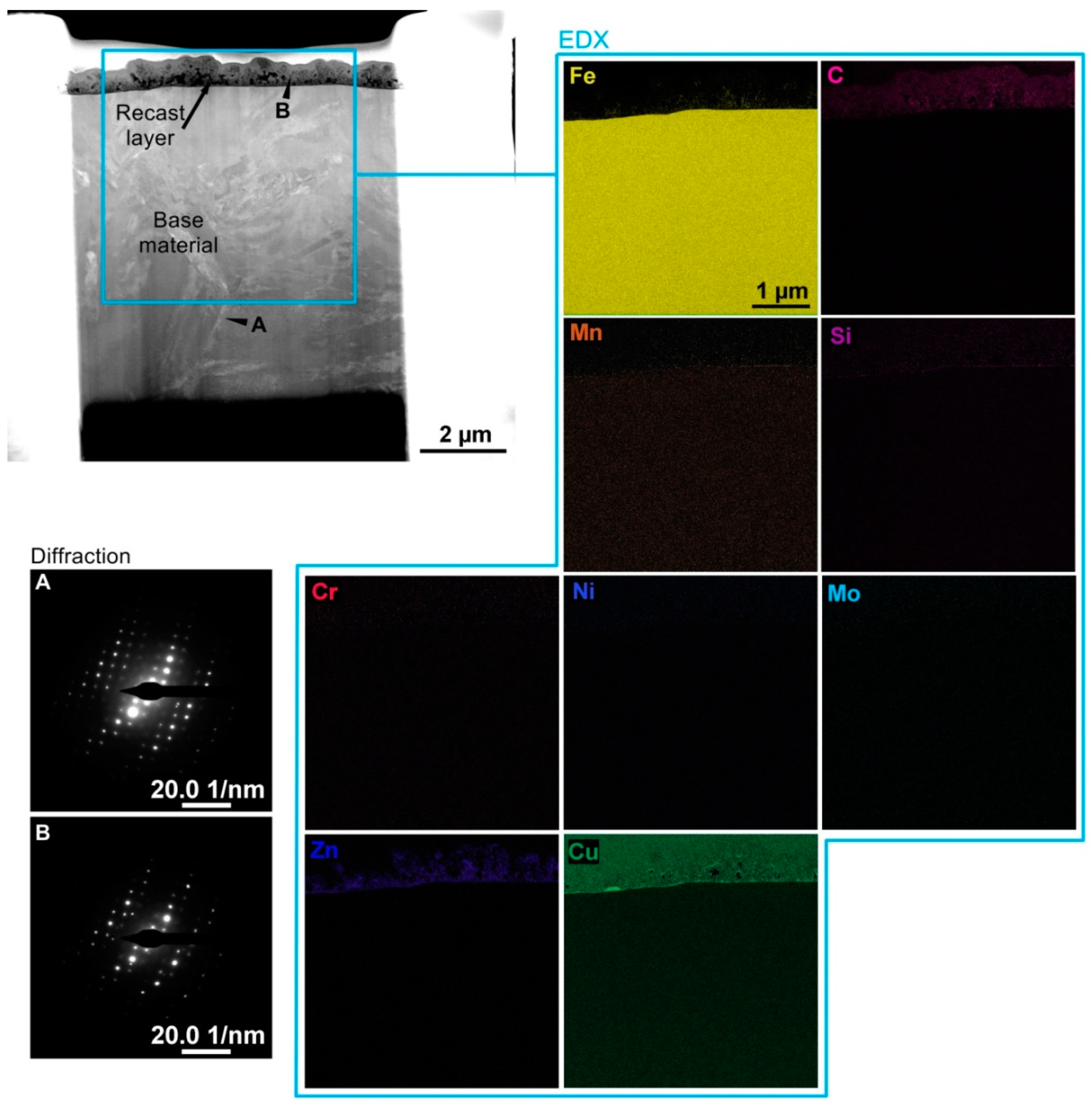
Due to the very high temperatures 10,000–20,000 °C [
3] incurred during the WEDM, the surface layer, the so-called recast layer, is completely melted at the cut point and then very quickly cooled by the dielectric fluid flow. As a result, it is transformed and very distinctive microstructural differences from the base material occur. The recast layer thickness and its multiple occurrence on the workpiece surface are determined by many different factors. It is primarily a mechanical and physical property set of the machined material, but also parameters of the machine setting, the number of cuts made, etc. [
4].
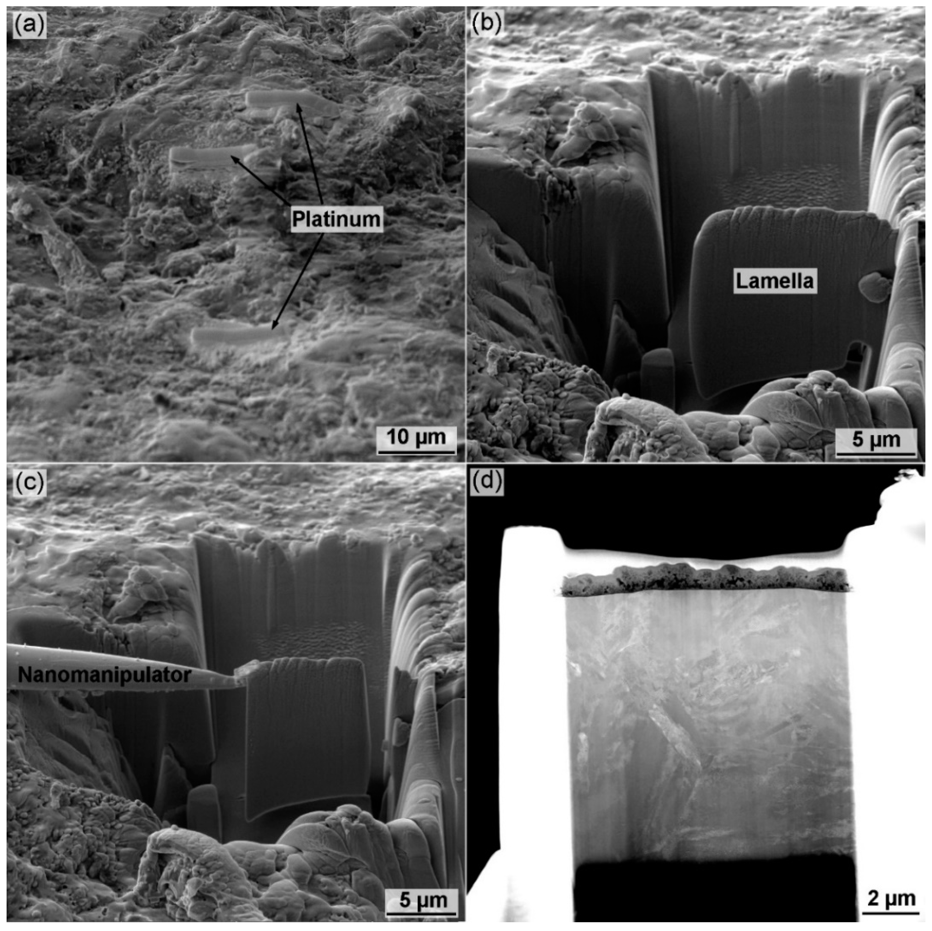
Klink [
5] in the study about the WEDM dressing and truing of diamond grinding wheels, fine grained metal bonded, also focused on the examination of the damage of a thermal grit surface and the graphitization of diamond. For the investigation of the amount of the graphitization, a crystallographic analysis was employed. To carry out this analysis a tiny electron transmission microscope (TEM)-lamella was produced of one eroded surface diamond grit by the focused ion beam (FIB). This helped reveal three carbon layers under two preparation layers, the inner layer crystalline structure and the outer layers amorphous structures, which indicated graphitization. Huang et al. [
6] researched the microstructure analysis of the steel surface of the martensitic stainless fine-cut by WEDM. During the experiments, they focused on the analysis of the TEM-microstructure of finished surfaces as well. To carry it out, cross-section and plain-view TEM-samples were produced. For their preparation, the ion milling and dimpling processes were employed to make a small hole in the center of the disc sample, which enabled examining the microstructures with the help of TEM and energy-dispersive X-ray spectroscopy (EDX). Moreover, from the output of the TEM study, a heat-affected zone, specified as the white layer, was found in the surface layer, and a few spherical deposits were also registered. Klocke et al. [
7] studied the white layer structure and composition in the WEDM process. To analyze the white layer metallurgical structure a thinFIB-lamella was produced utilizing the FIB technic. Meanwhile, TEM characterizations were performed, and the energy-filtered TEM images were obtained using a Gatan GIF system. While analyzing the carbon and recast layers, the FIB-lamella becomes thinner from the left to the right. The thin lamella outputs in an improved quality of the image, and subsequently a comprehensive analysis was carried out in the lamella’s very right part. Zhang [
8] focused on the impact of WEDM parameters on the integrity of the surface of nanocomposite ceramics, where he studied the microstructure. A TEM micrograph analysis was employed in the study, which displayed the fine-grained microstructure of the TiN/Si
3N
4 composite and TiN particles were allocated throughout Si
3N
4 matrices. It was also evident, that surfaces of Si3N4 particles were fully coated by TiN particles. Huang et al. [
9] investigated the rough-cut surface characteristics of tempered and quenched martensitic stainless employing WEDM. The TEM examination was done using the cross sectioned samples obtained from the samples tempered at 600 °C and with appropriate mechanical properties (strength, toughness, and hardness). With the help of these TEM specimens, an amorphous layer was detected on a few parts of the furthermost surface of the cut with randomly distributed fine crystalline particles inside it. While the examination of the recast layer, spherical electrode deposits, and a lot of one of the deposits of the wire-electrode material at the gas void side were detected in it, which were evident on the dark- and bright-field TEM micrographs. Murray et al. [
10] was interested in the TEM analysis on the WEDM surface of a single-crystal silicon. For the experiments, focused ion beam machining was carried out to produce a lamellar out of one of the machined holes. Since it was impossible to make a lift out from the whole bottom surface because of the entry angle of a manipulator, an “L” shaped lamellar was produced from the top edge of the hole. Jose and Shunmugam [
11] investigated the white layer built on the WEDM Ti6Al4V surface due to the surface quality and the component life. It was found, that the phases detected in the white layer are organized in the microstructure of the fine lamellar. The microstructure of the lamellar was formed as an output of plain cooling from the above β transus temperature. The amorphous phase was detected because of the oxygen high affinity in the microstructure of higher cooling rates and the fine lamellar in the WEDM process. Moreover, the rise in hardness was found because of the grain structure of a very fine lamellar detected in the white layer. Liu et al. [
12] studied crystallography, compositions, and characteristics of the white layer by the WEDM of a nitinol shape memory alloy. For the TEM analysis, the EDM specimens at the main cut were selected due to the ability of the main cut to produce a thick white layer. For the preparation of the electron transparent TEM specimen, a variation of the FIB in situ lift-out method was utilized for TEM foil producing. Throughout the study, the TEM analysis was employed to examine the white layer microstructure and crystallography and heat affected zone by the WEDM of Nitinol. Sanchez [
13] presented computer simulation software for the analysis of error in wire electrical discharge machining of taper-cutting. Punturat [
14] in his study focused on influence of major process parameters on the cut surface characteristics in the wire electrical machining of silicon. Chaudhari [
15] in his work investigated the surface integrity of WEDM-processed nitinol samples.
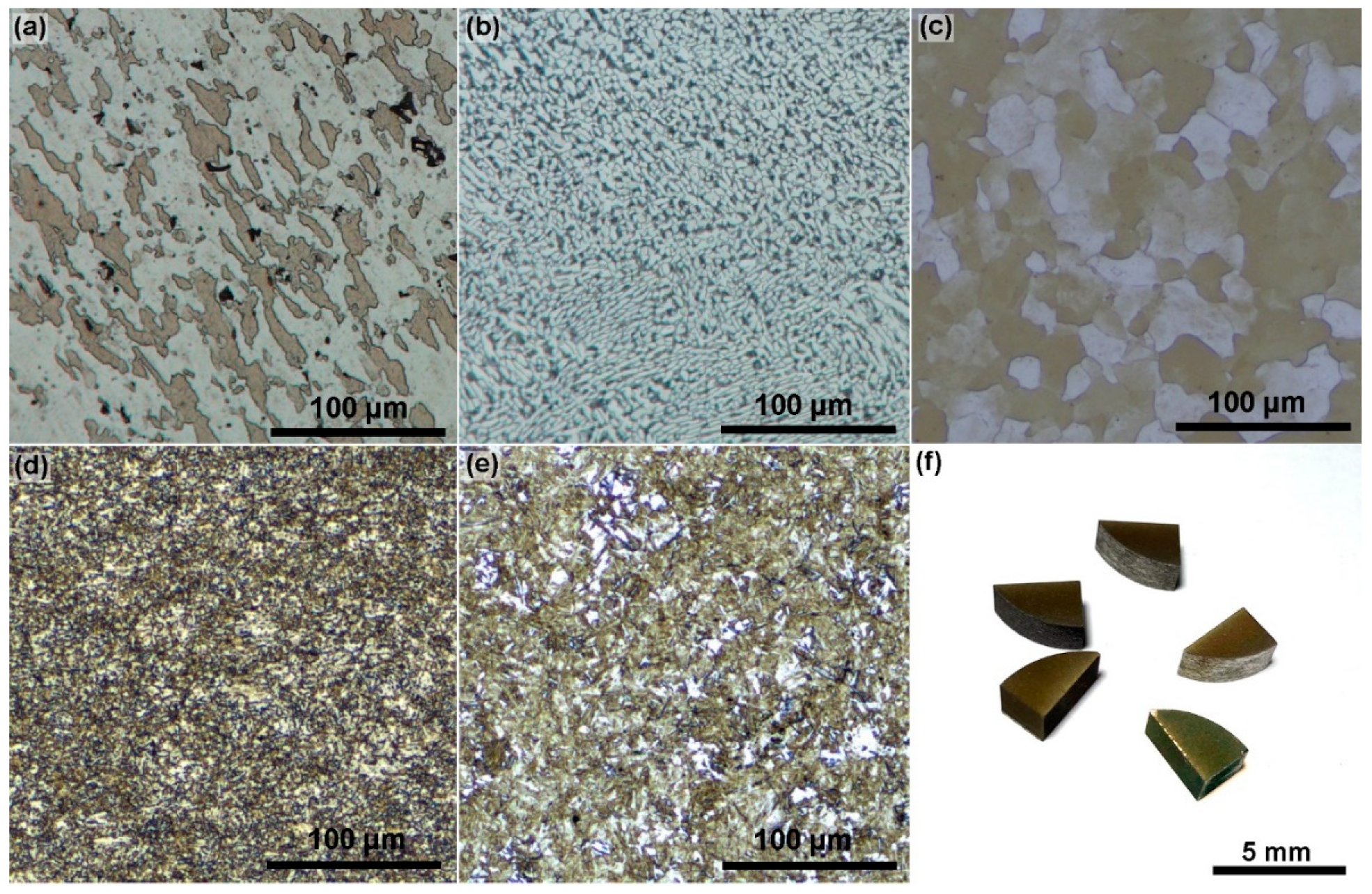
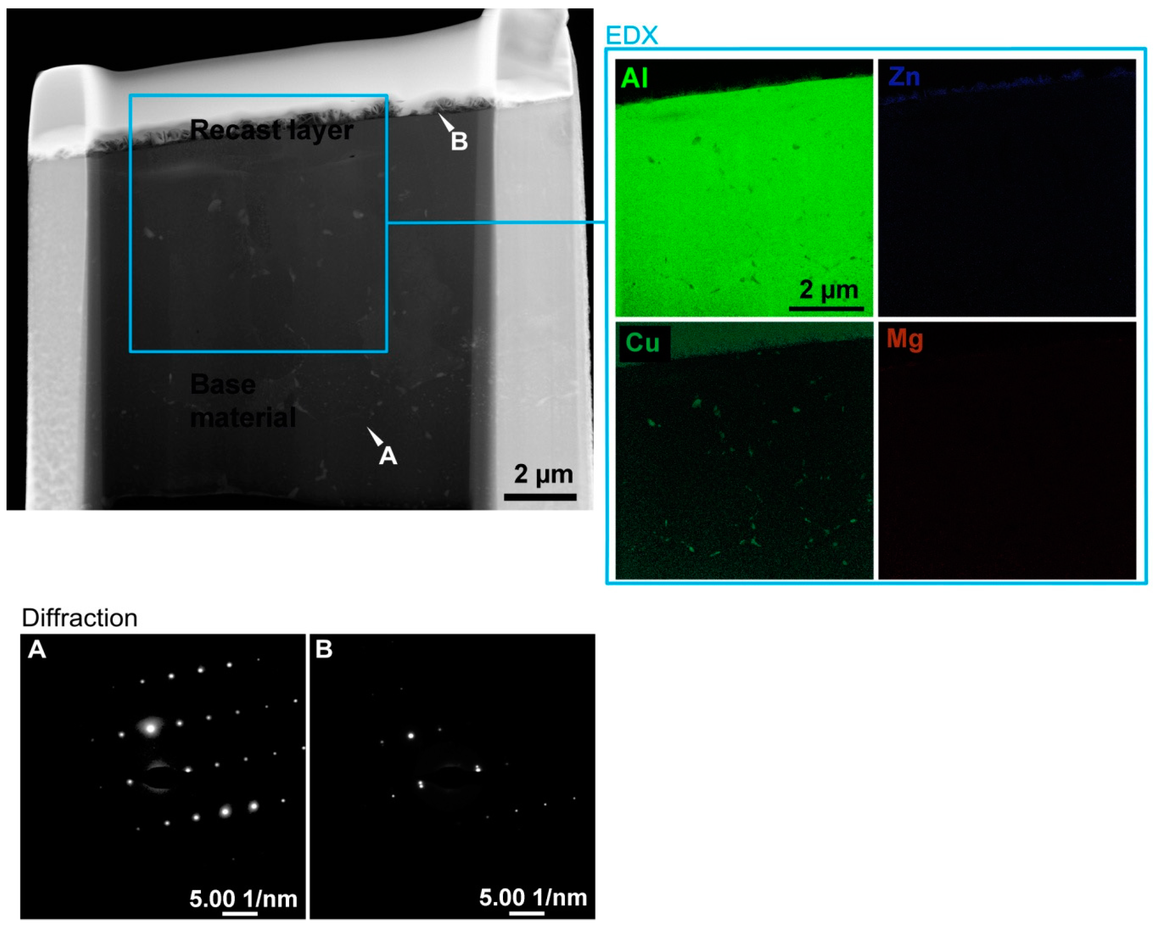
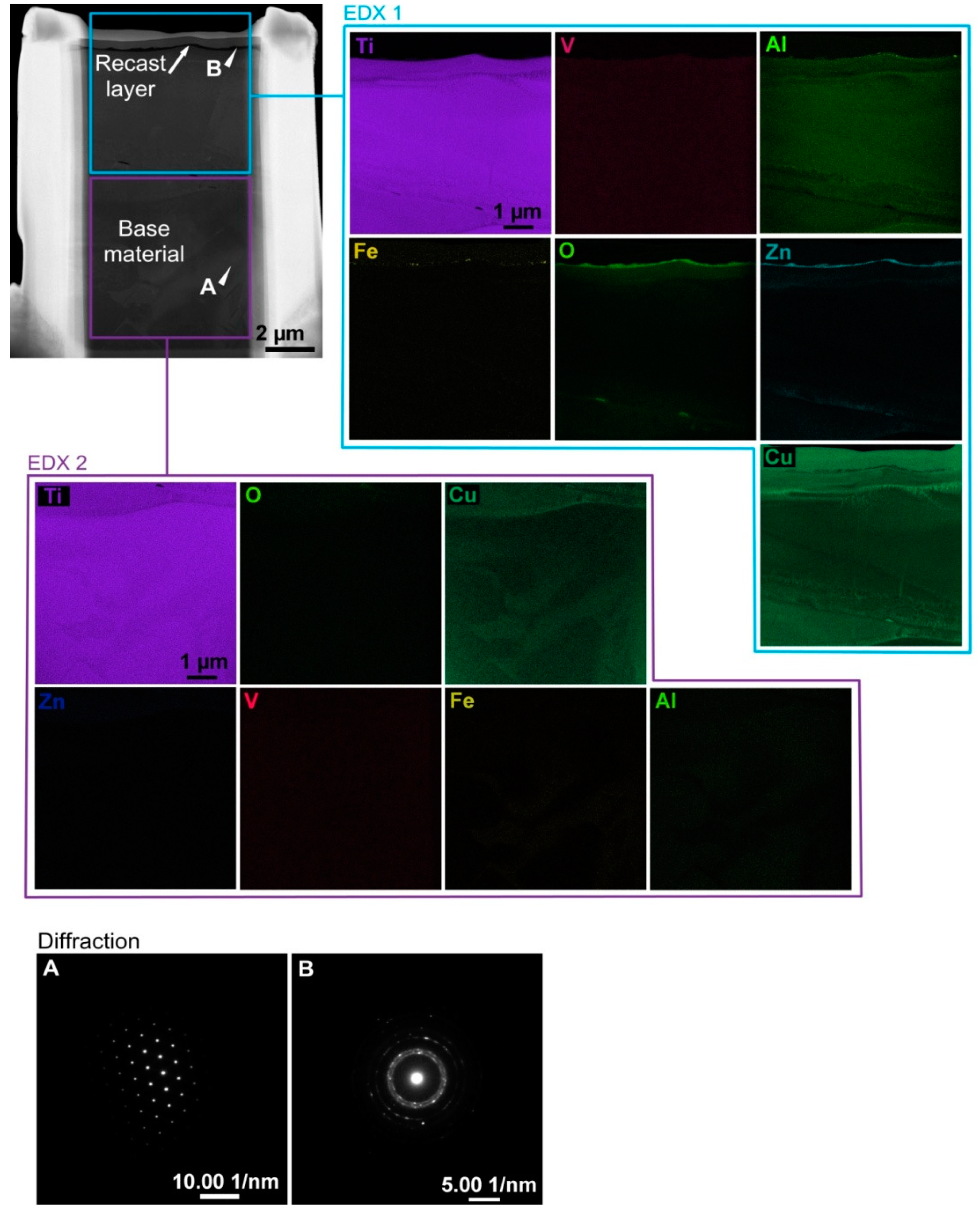
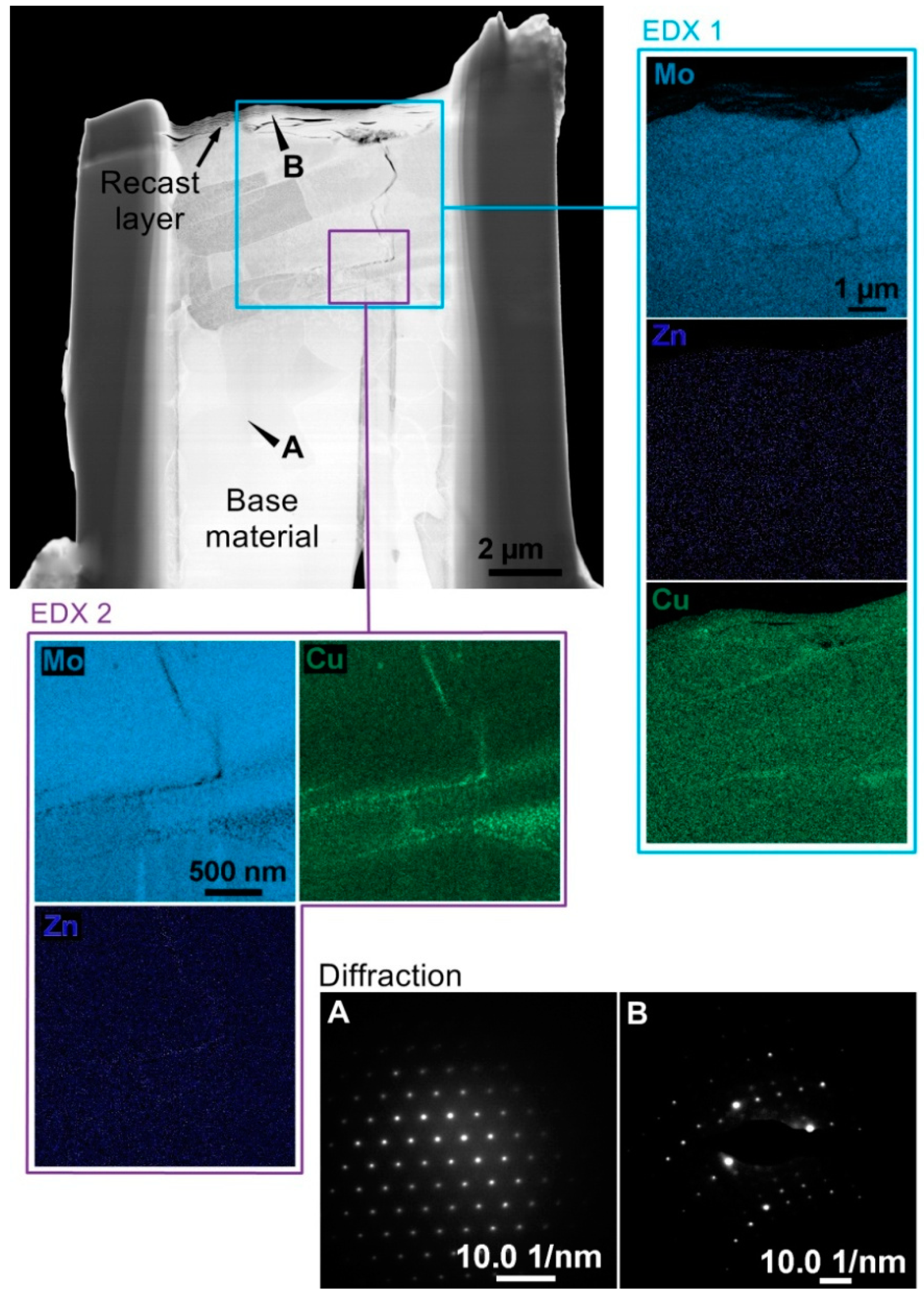
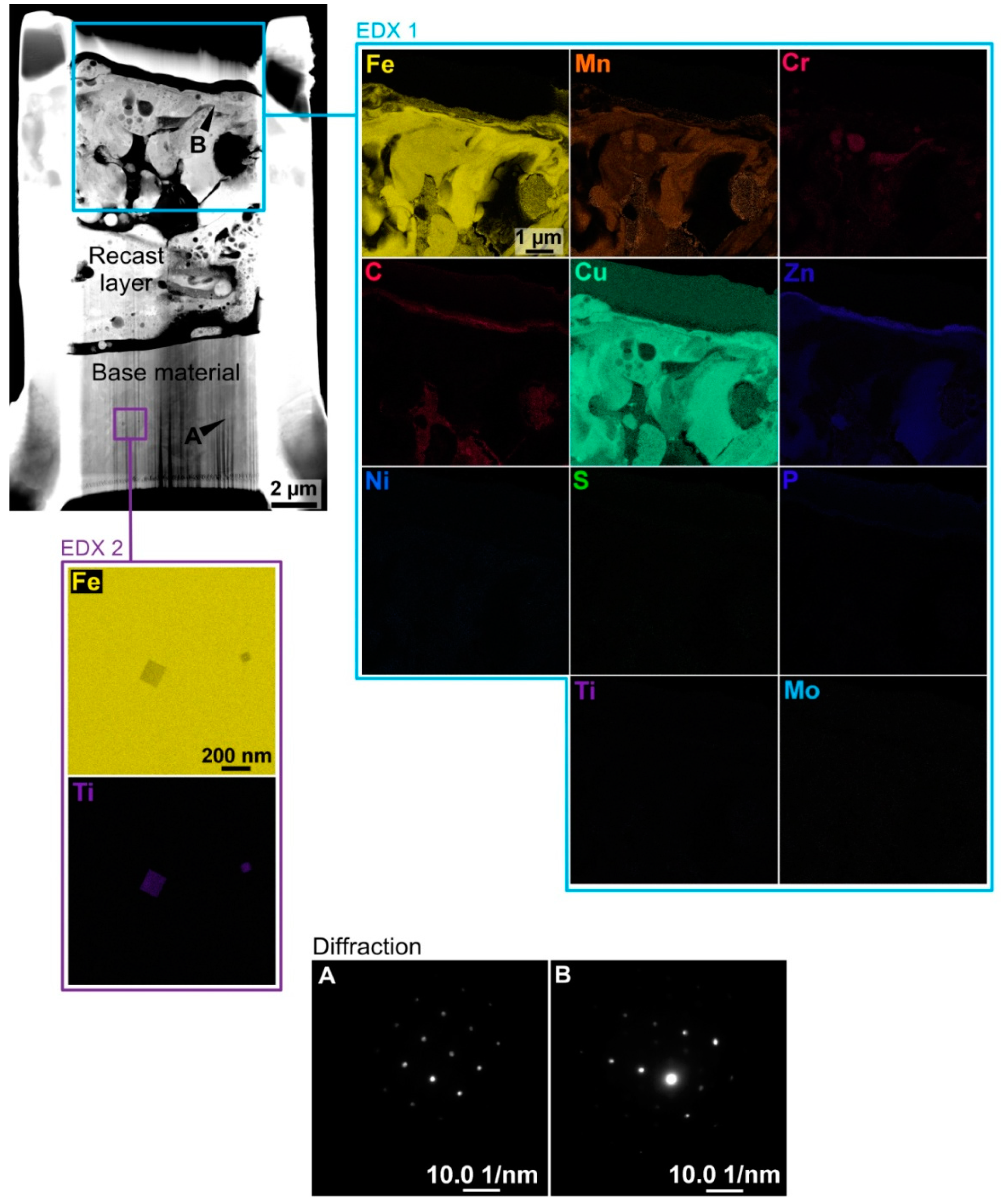
Since the recast layer affects the wear, fatigue, and corrosion of the electro-erosion machined parts, it is necessary to study this phenomenon in detail, since understanding it can lead to an increase in the lifetime of the manufactured parts. There are several studies dealing with these microstructure changes in the recast layer, but only for a few materials, with no complex comparison of mechanically and physically different materials. Therefore, in order to make a detailed and comprehensive comparison of alloys, pure metal, and hard-to-machine steels, this extensive study was aimed at mapping the microstructural changes in the recast layer and its boundary with the base material.

 ,
, 


