Article

A Data-Driven Machine Vision Framework for Quality Management in Photovoltaic Module Manufacturing

Department of Industrial and Systems Engineering, Dongguk University-Seoul, Seoul 04620, Republic of Korea
*
Author to whom correspondence should be addressed.
Machines 2025, 13(4), 285; https://doi.org/10.3390/machines13040285
Submission received: 10 February 2025 / Revised: 27 March 2025 / Accepted: 28 March 2025 / Published: 31 March 2025
(This article belongs to the Section Advanced Manufacturing)

Abstract

:
As renewable energy production grows, the photovoltaic (PV) module manufacturing process has received worldwide attention. In 2019, the total sales of PV modules were 1.7 billion U.S. dollars, and 78.7% of PV modules were made in South Korea. However, Korean manufacturers are facing high production costs due to high domestic labor costs and long-distance raw material procurement, making it difficult to produce price-competitive PV modules. In this situation, the best alternative for Korean manufacturers to gain a competitive edge is to produce high-quality PV modules. To this end, this study is going to propose a novel data-driven machine vision framework for the quality management of a PV manufacturing process consisting of seven stages, including tabbing, auto bussing, electro luminescence (EL), laminating, fame station, frame, and junction box. Particularly, the framework uses machine vision to analyze image data collected from an actual PV module manufacturing facility in South Korea. Autonomous decision-making algorithms are devised to recognize incorrect patterns of PV modules in terms of product quality. This experiment shows that the proposed framework enables the detection of PV module defects in electroluminescence (EL) and tabbing operations with a fault detection accuracy of over 95%. Therefore, the proposed framework enables a reduction in the number of defects, and this helps to improve quality loss during the PV module manufacturing process.

1. Introduction

Recently, there has been worldwide attention on the establishment of a new policy on carbon neutrality. For example, twenty leaders of the biggest countries in terms of economy have agreed to carbon neutrality at the G20 summit in Rome [1]. In addition, the United Nations (UN) set the goal of affordable and clean energy use and tries to investigate clean energy resources involving solar, wind, and thermal for the sustainable life of humans [2]. As a result of these global efforts to use renewable energy, the global solar power generation capacity has increased from 83.3 GW in 2016 to 228.4 GW in 2022, at an average annual growth rate of 20.73% [3]. The global solar power generation market has expanded from USD 86 billion in 2015 to USD 422 billion in 2022, and it has grown on average by USD 42 billion over 8 years [4]. Considering that the global solar power market is continuously growing at a compound annual growth rate (CAGR) of 12.17%, the market size is expected to reach approximately USD 460.5 billion by 2030 [5]. In South Korea, the solar power generation market is expected to grow from USD 2.8 billion in 2020 to USD 3.7 billion in 2025 at a CAGR of 5.8%. The solar power generation market is classified into a balance of system (BOS), modules, and inverters by components; moreover, among them, modules are expected to grow from USD 33.3 billion in 2020 to USD 49.8 billion in 2025 with a CAGR of 8.3% [6].
In response to the global increase in demand for solar energy, the Korean government is also announcing various policies to expand solar energy power generation facilities and manufacturing equipment. In 2022, the Korean government selected the solar power technology sector as one of the 10 carbon-neutral technology innovation sectors in the 2050 carbon neutrality promotion strategy [7]. The announced technology innovation policy uses the fourth industrial revolution as a keyword, and this is being shown in the innovation of manufacturing processes and reduction in production costs using artificial intelligence (AI) technology in the solar module manufacturing industry. In other words, the need to secure price competitiveness in the domestic solar power manufacturing sector is increasing by introducing operational automation equipment to solar power manufacturing lines or next-generation production facilities based on AI and big data in South Korea [8].
In general, the PV module manufacturing process has a sequential manufacturing process structure, including the tabbing process for connecting solar cells, the frame process for assembling frames to the manufactured individual modules, and the junction box mounting for connecting busbars and junction box terminals [9]. In other words, since the connection between individual PV modules is the main task of the PV module manufacturing process, defects in each solar cell and module ultimately affect the power generation performance of the PV system [10,11]. In addition, the occurrence of defects results in additional work and increased production costs [12]. In order to improve the productivity of the PV manufacturing market and develop new technologies such as high-efficiency PV cells, research and development (R&D) is being actively conducted by the government, industries, and research institutes in multiple countries involving China [13], Taiwan [14], and South Korea [15].
This study aims to propose a data-driven machine vision framework for the quality control of the PV module manufacturing process to improve PV system performance and reduce manufacturing costs. The advantage of machine vision is that it can detect defective products using the latest artificial intelligence technology (or computer vision technology such as convolution neural network (CNN)) by installing monitoring sensors and equipment without changing the existing manufacturing process. This is a practical approach that can be used to improve quality in small and medium-sized manufacturing environments that use old machines due to investment cost issues. To this end, operational data and electroluminescence (EL) image data from the manufacturing process and equipment are collected and analyzed using the proposed machine vision technology. In addition, the impact of machine vision analysis on quality and productivity improvement in the main process of PV module manufacturing is investigated. Experiments are conducted at the PV module manufacturing facility in South Korea, and the proposed framework is utilized to detect PV module defects in electroluminescence (EL) and tabbing operations. As a result, the proposed framework can contribute to improving the quality of PV modules and the profitability of manufacturing facilities by reducing the number of defects.

2. Materials and Methods

2.1. Manufacturing Process for Photovoltaic Modules

The photovoltaic (PV) system utilizes a methodology to transform solar radiation to direct current via multiple PV modules [16]. Generally, the PV module consists of a frame, front and back covers, encapsulant, solar cells, and a junction box [17,18]. Among the components, the solar cell is the most important component because it transforms photon energy ( E λ ), which is associated with a certain wavelength to electricity via semiconductors (i.e., p-type and n-type silicon layers). Equation (1) denotes the photon energy formula associated with wavelength λ , Plank’s constant h, and speed of light c [19].
E λ = h c / λ
Note that an electron-hole pair with a photon that has greater energy than a bandgap between the p-type and n-type silicon layers can generate electricity. In other words, if a solar cell receives sufficient sunlight, electrons in the silicon layers are ejected from the n-type silicon layer and moved to the external wire via the p-type silicon layer. This results in the generation of a direct current. These physical reactions produce electricity, and the resulting power output varies depending on how efficiently the solar radiation input from the outside is absorbed. The efficiency of the power generation varies depending on whether the crystal structure or materials such as Cadmium Telleride (CdTe) and CuInGaSe2 (CIGS) are used.
For efficient production of PV modules, the manufacturing process generally has a sequential manufacturing process structure [17,18], which is shown in Figure 1 along with seven operation stages, including tabbing, auto bussing, electroluminescence (EL), laminating, frame station, frame, and junction box mounting.
As shown in Figure 1, the tabbing operation is the first operation to connect multiple solar cells in a row by soldering so that it generates a string cell [20]. Either infrared soldering or a heat gun is used in this operation to complete the task within a few seconds with enough adhesive strength between the ribbon and solar cells. Auto bussing is the operation employed to produce a solar module by connecting a panel string with multiple solar cells to a board [21]. Since the panel string has the input and output nodes, the solar module can have different connection shapes (e.g., a single string or parallel string) according to solar module design. EL is used to conduct a test to identify microcracks on a solar module by using a polarization current, which makes a solar cell emit EL radiation [22]. From this electrical stimulation, engineers are able to acquire a high-resolution image with which to detect the microcracks. In the laminating operation, the panel string is covered by an encapsulant under high pressure and temperature. The machining parameters (i.e., pressure level and temperature) are determined using a type of an Ethylene Vinyl Acetate (EVA) sheet and its curing condition [23]. The frame station makes a frame for the encapsulated panel, and the frame operation involves attaching the encapsulated panel string to a PV frame. Junction box mounting is the last operation and involves attaching the junction box to the rear side of the frame via sealant or adhesive. The junction box should be linked to a busbar of the solar string so that generated electricity can be transferred to an external electrical device [24].

2.2. Quality Management in Photovoltaic Module Production

Quality management in PV module production is needed to manufacture a PV module with long-term reliability [11]. To this end, cause and effect analysis is conducted to identify the factors of the electricity generation efficiency loss of a PV module based on data collected from seamless monitoring of the manufacturing process [25]. As mentioned in Section 2.1, the manufacturing process consists of seven major sequential operations so that loss from a former operation is additive to the next operation. Five major defects occur throughout the seven operations as follows: (1) 36% are related to the connections between solar cells or other internal electrical components; (2) 32% of the defects are caused by cracks in the front cover or encapsulant; (3) 12% of the defects are related to the junction box installation or cabling; (4) 10% are caused by failures in the solar cell itself; and (5) 10% are caused by failures in the back panel connections [26]. Although these figures may vary depending on individual manufacturing environments, it is true that failures are relatively frequent because solar cells and other small components are connected by small welds [27,28].
As an example of the tabbing operation, there exists either an unsoldered wire issue or a wire breakout issue while multiple solar cells are connected in a row by soldering under various manufacturing conditions such as solar cell property and temperature [29]. In the laminating operation, air bubbles between an Ethylene Vinyl Acetate (EVA) sheet and the panel string can be infiltrated, which results in a reduction in the solar radiation absorption of the PV module [30]. Another defect is associated with micro-cracks on a silicon wafer, causing the failure of an entire PV module [31]. Since a silicon wafer (i.e., n-type silicon layer or p-type silicon layer) is a thin component, its internal micro-crack can be extended to damage the PV module by continuous vibration or tiny shocks. To avoid this defect, the micro-crack on a silicon wafer is generally inspected via infrared light at the electroluminescence (EL) operation stage. In the case of silicon wafers, they have relatively high transmission characteristics for wavelengths of about 1 µm. Using this principle, by illuminating the wafer with near-infrared light and obtaining an image from the opposite side, an image can be obtained that can identify micro-cracks that exist inside the wafer and cannot be detected under normal lighting conditions [32].

2.3. Quality Management Framework Using Data-Driven Machine Vision

The data-based machine vision framework for quality management of the PV module manufacturing process proposed in this study is illustrated in Figure 2. Machine vision refers to a solution that automatically detects defects in the product appearance using a machine learning model and takes appropriate measures for the manufacturing line based on the results. As shown in Figure 2, the proposed machine vision framework consists of three main modules.
In Figure 2, the proposed framework monitors the appearance of PV module components (solar cells, strings, frames, etc.), particularly in electroluminescence (EL) and tabbing operations, via camera sensors (or vision sensors) in real time. GE34GC Monochrome and GE50GC Monochrome cameras supporting 100-m transmission and hardware image processing acceleration are used in the framework. Table 1 describes in detail the specification of the machine vision camera sensors.
Figure 3 and Figure 4 show the machine vision installed in EL and tabbing operations. The proposed framework has the advantage of being able to detect product defects by installing only camera sensors and monitoring equipment without changing the existing manufacturing equipment.
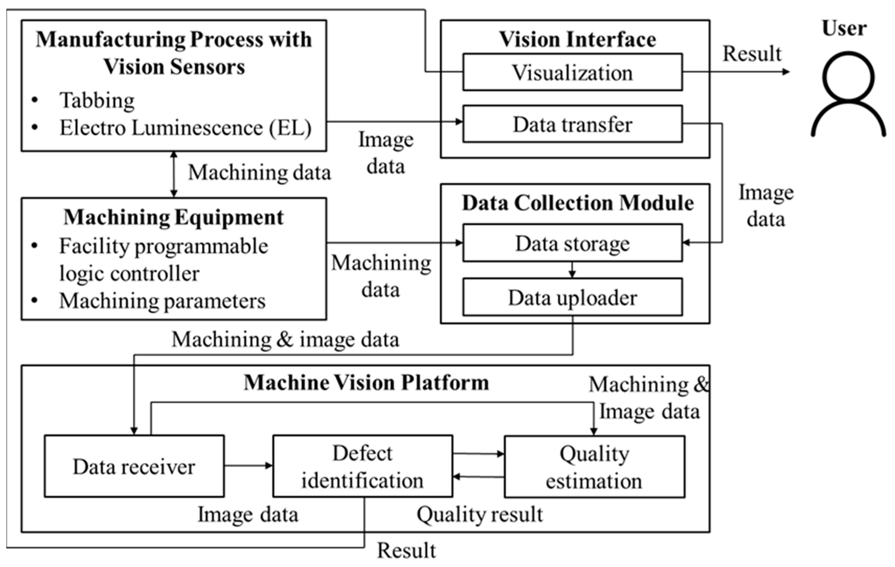
The PV module images collected by the vision sensors are transmitted to the data collection module through the interface and stored in the database for real-time defective product detection and judgment, subsequent artificial intelligence algorithm learning, and product quality management. During this process, the PV module manufacturing environment information (machining parameters and PLC control information) provided by the manufacturing equipment is also stored in the database. Image data acquired through the machine vision are transmitted to the data collection module in real time through IoT (Internet of Things). In particular, the IoT is developed as an appliance consisting of manufacturing analysis data collection and protocol standardization functions by utilizing the Edge box gateway. This appliance standardizes structured and unstructured data generated in the module manufacturing process and classifies them into a specific type of analysis dataset. In addition, it includes a middleware operating system for storing relational databases (RDBMSs), time series databases (TSDBs), and file systems (File DBs) depending on the data characteristics. The stored machining and image data are transferred to the machine vision platform, and in this process, the Quality Estimation and Defect Identification modules are responsible for extracting defective products using artificial intelligence. These modules analyze images to detect defective products with different patterns from existing products and make predictions about possible defective products. It utilizes the real-time inference function, which is a key function that can quickly discover the effects of introduction by applying artificial intelligence to the manufacturing site [33]. By combining real-time process data and inspection (image) data, a big data-based learning model is created, and the convolutional neural network (CNN)-based inference engine functions to enable immediate anomaly detection and quality prediction in the manufacturing field (see Section 2.3.1 and Section 2.3.2 for details). This field data inference framework is used as a tool for rapid problem-solving by detecting various and complex causes of defects that interfere with production in advance. Ultimately, the machine vision platform has the function of checking the PV module components and detecting defective products by comparing their characteristics with normal products.

2.3.1. Defect Detection in the EL (Electroluminescence) Operation

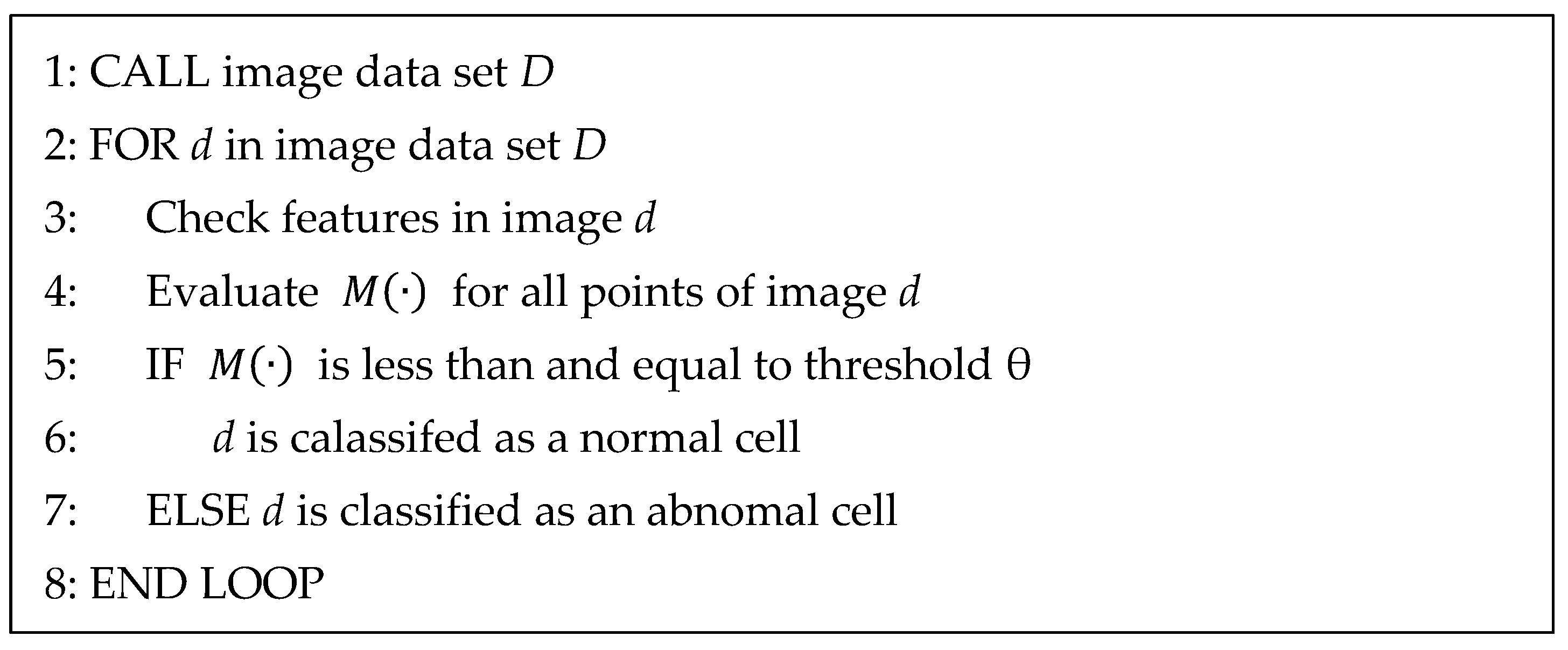
In EL operation, a three-step machine learning model is applied to detect defects. First, in the pre-processing stage, an original image is subjected to geometric image transformation operations such as centering and data augmentation to ensure that only the regions with cells are selected. Second, the unsupervised anomaly segmentation technique is used to detect cells that are different from the normal PV cells [34]. Third comes the classification of defected PV cells into four categories, such as crack, dark spot and dark area, and solder dark defects. The purpose of anomaly detection (or one-class learning) is to learn the distribution of normal samples so that when abnormal samples come in, they can be classified outside the learned distribution (i.e., outlier or anomaly detection) [35]. One characteristic of this is that it can significantly improve classification performance by combining a small number of abnormal data during the model learning process. In order to learn about the characteristics of normal cells at position (i, j) in an image, let X i j = x i j k , k 1 , N be the set of embedding vectors for position (i, j) learned through N normal cell images [36]. If X i j follows a multivariate Gaussian distribution N ( μ i j   ,   Σ i j ) with sample mean μ i j and sample covariance Σ i j , the set of embedding vectors for location (i, j) can be summarized as shown in Equation (2). Notice that ϵ I serves as a normalization term to make Σ i j full rank and invertible.
Σ i j = 1 N 1 k = 1 N x i j k μ i j x i j k μ i j T + ϵ I
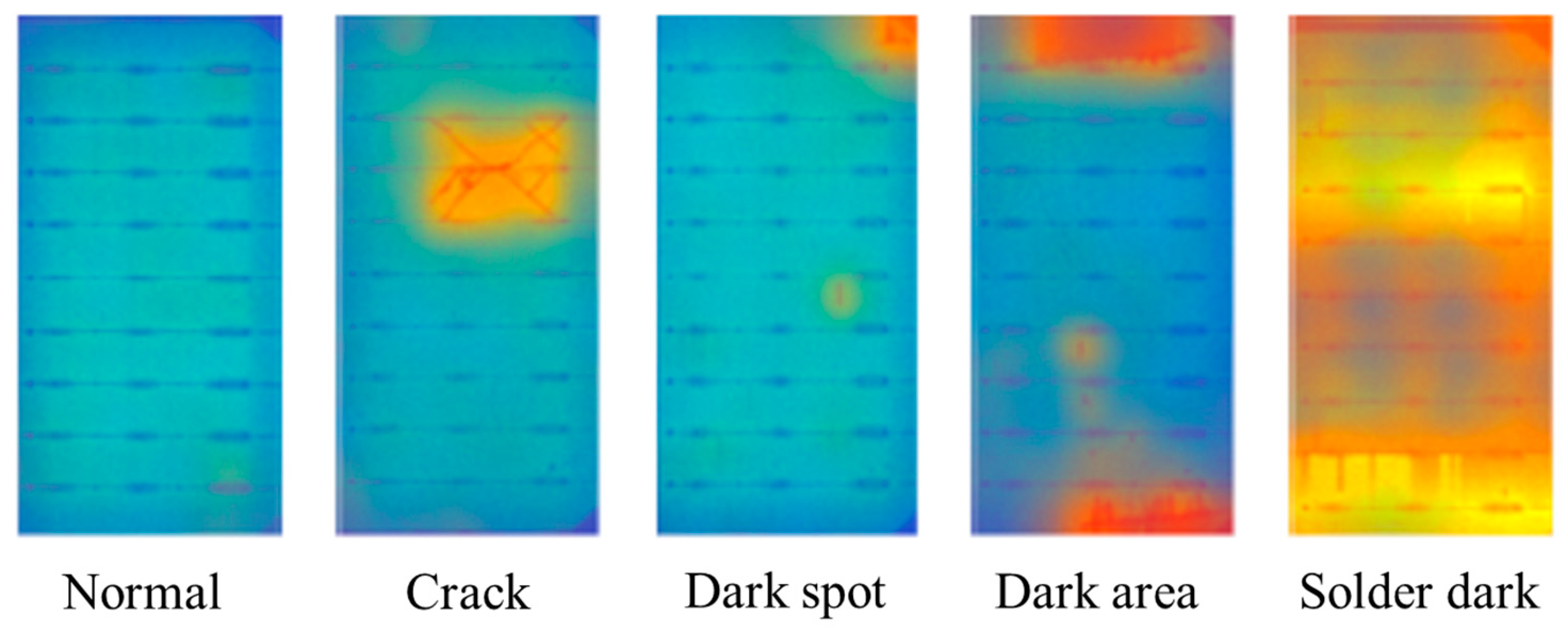
Figure 5 represents the anomaly detection of a PV cell. If M · , which is the Mahalanobis distance described in Equation (3), is greater than the threshold (θ), it is considered an outlier (i.e., abnormal PV cell).
In general, the Mahalanobis distance is an unsupervised method that is used to calculate the distance between two points, similar to the Euclidean distance, but it calculates it by finding the inverse matrix of the covariance calculated from collected data. M x i j refers to the distance in the probability distribution of how far the observed value ( x i j ) is from the original mean ( μ i j ) at (i, j). Since high scores on this map indicate anomalous areas, the final anomaly score for the entire image is the maximum value of the anomaly map, with defective components having high values.
M x i j = x i j μ i j Σ i j 1 x i j μ i j T
Figure 6 shows the average distribution of grayscale image values for 84 normal product images and 74 defective product images collected in the EL process. It can be seen that the abnormal products have a larger observation probability value from 180 to 210 on average, showing a difference in distribution from the normal products. The Mahalanobis distance calculation result, according to Equation (3), shows that the defective product images have a value greater than 0.00022. Based on this threshold (θ = 0.00022), defective products can be differentiated from normal products.
For the classification of abnormal PV cell images, ResNet50, which is a well-known deep learning model used in computer vision tasks [34], is adopted. As shown in Figure 7, defective components are classified into cracks, dark spots and dark areas, and solder dark defects. The sky blue color indicates a healthy part, while the orange color indicates where a defect has occurred in the part.

2.3.2. Defect Detection in the Tabbing Operation

Similar to the EL operation in Section 2.3.1, in the pre-processing stage, geometric image transformation operations such as centering and data augmentation are applied to the original image so that only the region of interest (RoI) is extracted. Additionally, the wire shape and number of lines are extracted to conduct a rule-based defect classification. The rule-based classifier continuously receives new information and processes it according to features they have already learned; particularly, the deep neural network model enables them to efficiently conduct the classification [
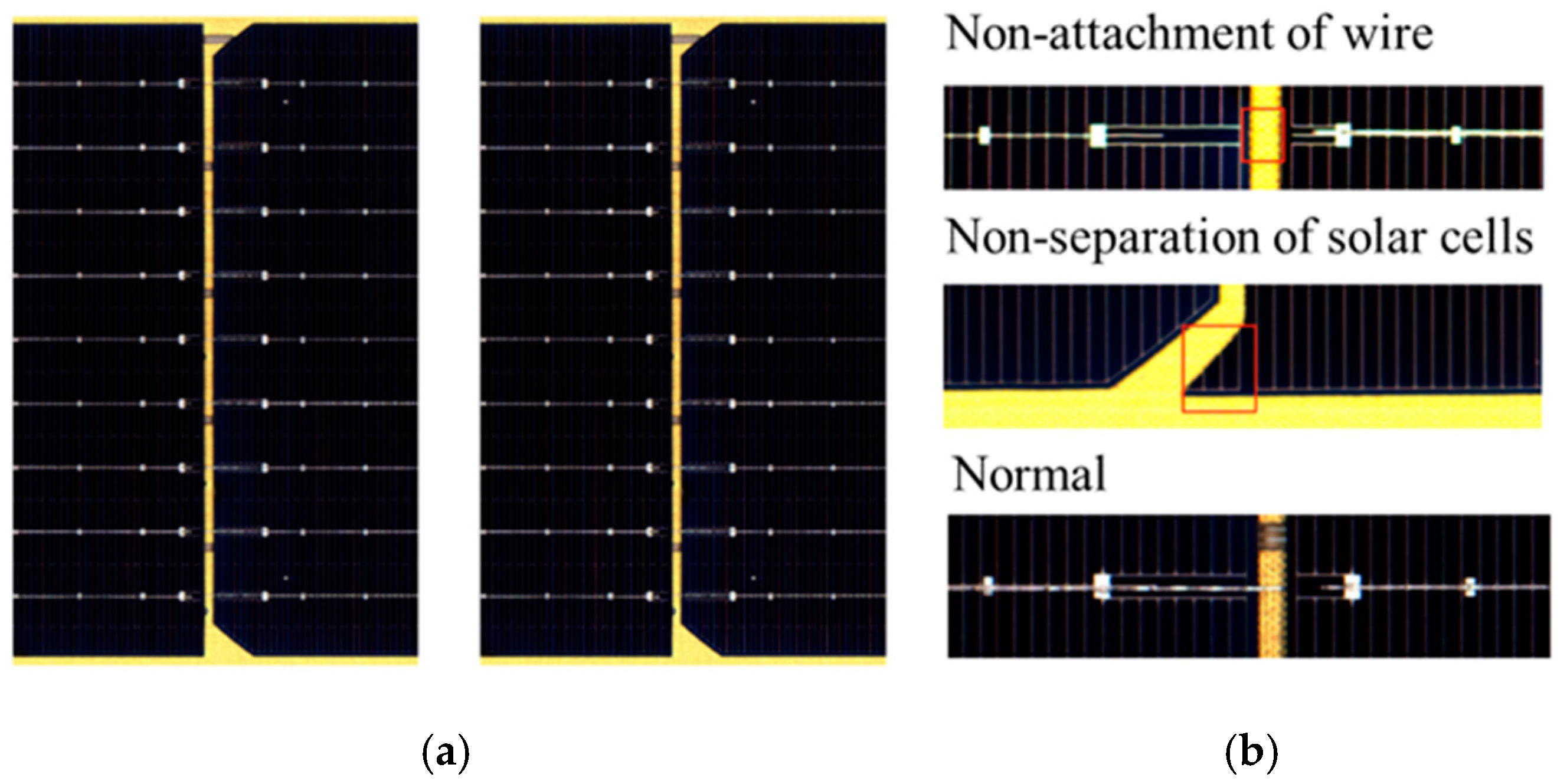
37]. As shown in 
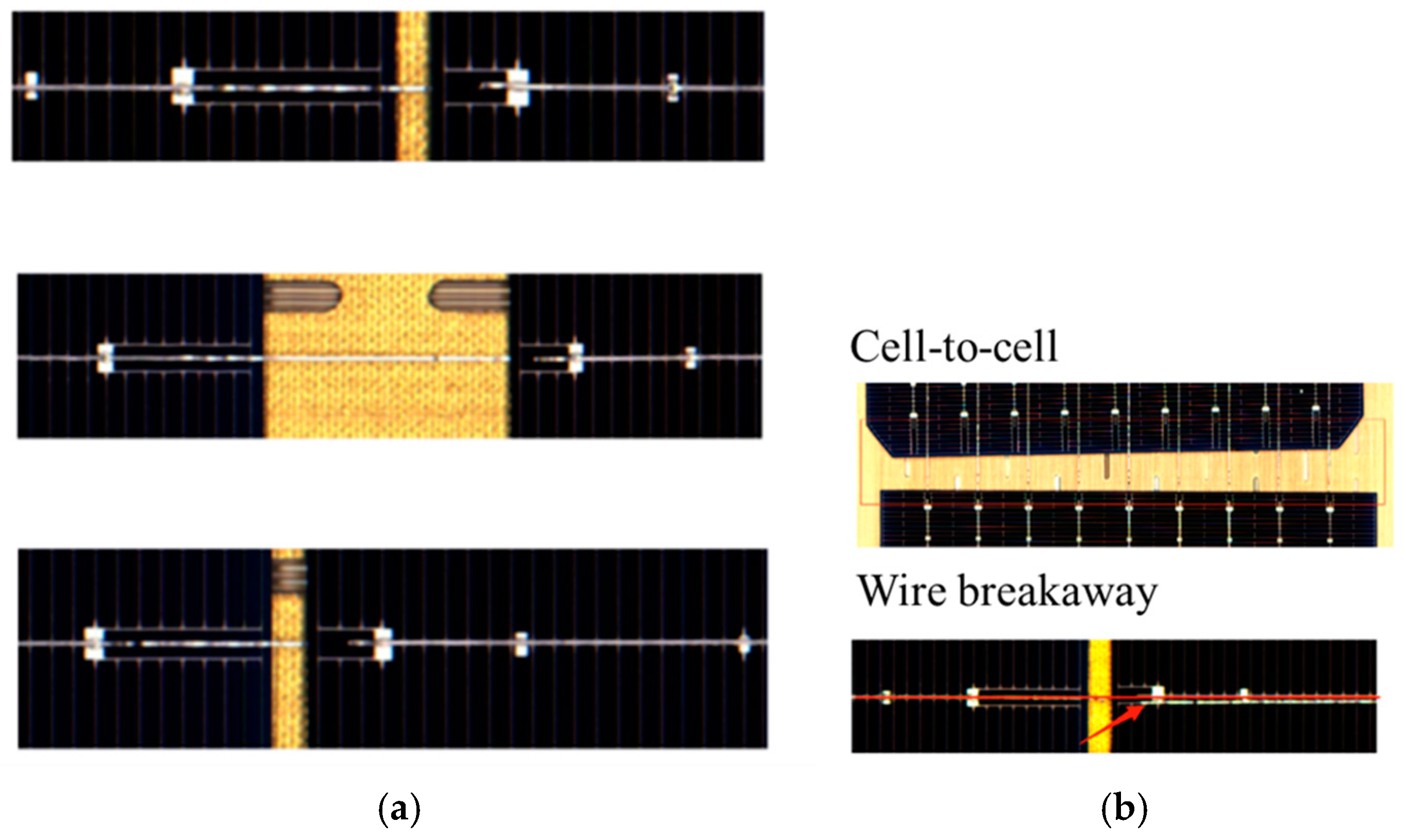
Figure 8, in the tabbing operation, the attachment of wires, separation of solar cells, and classification of normal PV panels are determined. The red box indicates the location where the defect is detected in Figure 8.
For the anomaly detection, class-imbalance learning is conducted to consider cases with different numbers of data samples. In fact, most machine learning models are established on the assumption that the ratio of data volume between classes is similar. However, if the imbalance is large during model learning, the learning is biased toward the class with a large number of data samples. For example, in binary classification such as vision images, when there are 90% of samples in the good class and 10% of samples in the bad class, classification performance can be improved by learning by balancing the number of data between classes. The random oversampling technique [38] is used with Equation (4) to add samples to the minority class by copying existing samples at random. R a d d is the ratio of adding samples; N a d d is the number of added samples; N n o r m a l is the number of images of normal products; and N a b n o r m a l is the number of images of abnormal products (i.e., defects). This cluster-based over-sampling (CBO) can deal with between-class and within-class imbalance simultaneously so that the detection performance for defective products can be improved even though the over-fitting issue may happen [39].
R a d d = N a d d / N n o r m a l N a b n o r m a l
Based on the balanced classes, the proposed machine vision platform performs the object detection using a convolutional neural network (CNN), which consists of an input layer, a hidden layer, and an output layer [40]. In order to configure the model, the dataset was first divided into a training set and a test set. The ratio of the training set and the test set was 7:3. The total number of images used for the model train was 110, and the total number of test images was 48 (see Table 2).
The image in the process has too large a pixel size; thus, if we use the image to construct a general CNN model, the computer memory will overflow. Therefore, the task of reducing the image size is performed first. The original size of the image is 5770 × 2912 pixels; however, the image was reduced to 600 × 300 pixels in order to train while maintaining the ratio of the image.
Next, the CNN structure was constructed. Keras was used as the deep learning library for constructing the CNN model. The model used a simple CNN model structure. First, three Conv2D layers were constructed, through which the image features were extracted without losing the spatial information of the image. Then, a max_pooling2d layer, which is a pooling layer, was added between each convolutional neural network, and the image features were reduced in size while being maintained. After this process, the multidimensional array was converted into a one-dimensional array through the flatten process, and classification was performed through the dense layer. The activation function used for the final classification is the sigmoid function.
y = 1 1 + e x
Equation (5) has a value between 0 and 1. When the x value learned in the proposed model is input, Equation (5) provides the y value, which is the classification result. This model is classified into two types of labels: normal product and defective product. Therefore, according to the classification criteria, if the y value is 0.5 or more, it is classified as label 1 (defective product), and if the y value is less than 0.5, it is classified as label 0 (normal product).
The model is trained through a total of 60 iterations with parameters described in Table 3. The optimizer uses Adaptive Moment Estimation (Adam), and the model loss is calculated using binary cross entropy (see Equation (6)). Binary cross entropy (BCE) is a loss function specialized for binary classification problems, and it is a method that imposes a large penalty on the model for making incorrect predictions. The calculation is calculated as follows, where y is the actual label, and p is the predicted probability that the data point belongs to a specific label class. For reference, the model training time is 3 min and 36 s.
B C E = 1 N i = 1 N y i log p y i + 1 y i log 1 p y i
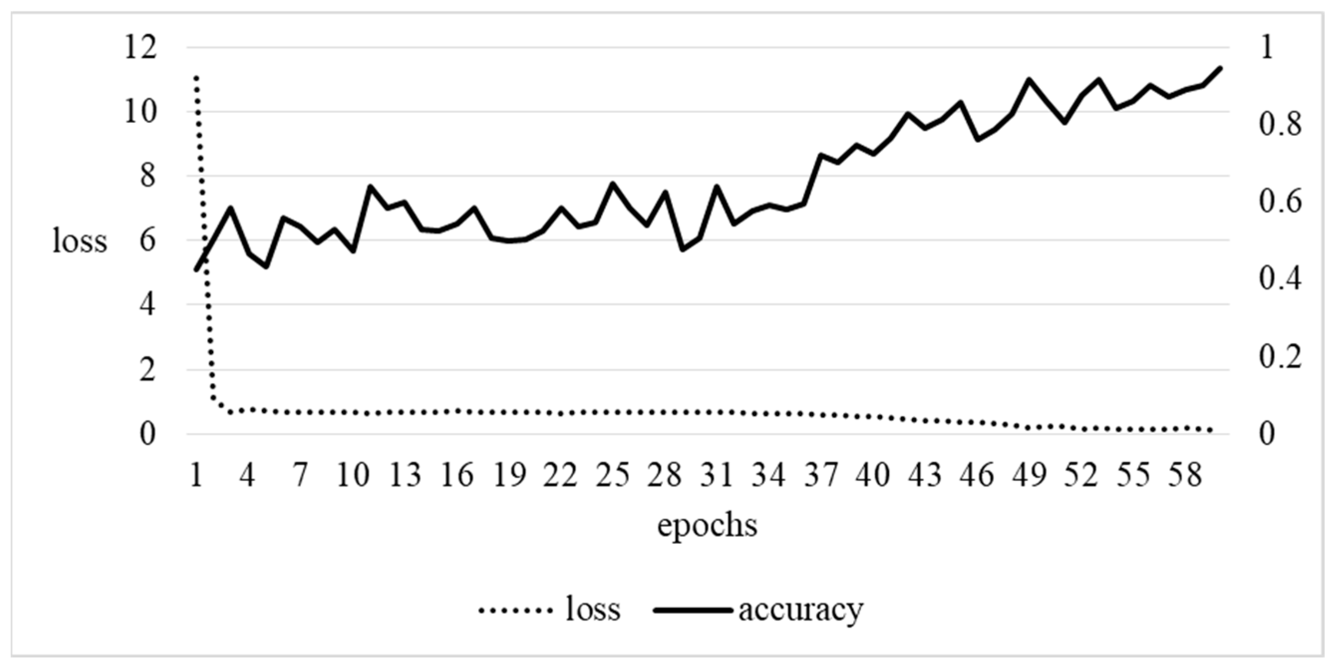
The learned model is used to make predictions on the test dataset. The test set consists of a total of 48 images, of which 25 images are normal data and 23 images are abnormal data. It takes less than 1 s to predict all 48 images. The accuracy and loss values according to learning are as shown in Figure 9.
Accuracy increases from 42% at the beginning to 94% through 60 repetitions. Loss shows a value below 0.2 after 51 repetitions through 60 repetitions. The learning results are as described in Table 4.
Based on the experimental results in Table 4, the model is evaluated in terms of accuracy, precision, recall, and F1-score.
A c c u r a c y = T P + T N T P + F P + F N + T N
P r e c i s i o n = T P T P + F P
R e c a l l = T P T P + F N
F 1   s c o r e = 2 × P r e c i s i o n × r e c a l l P r e c i s i o n + r e c a l l
TP means true positive, which means that something that is actually True is predicted as True, FP means false positive, which means that something that is actually False is predicted as True, FN means false negative, which means that something that is actually True is predicted as False, and TN means true negative, which means that something that is actually False is predicted as False.
Accuracy is the ratio of correct answers predicted in the entire sample, and in this model, 40 out of 48 data were correct; therefore, the accuracy is 83%. Precision is the ratio of things that the model predicted as True to things that were actually True, and the precision of this model is 100%. Recall is the ratio of things that the classification model judged as True among the samples that were actually True, and the recall of this model is 76%. The f1 score calculated through the calculated precision and recall values is 86.17%. Meanwhile, these results show that performance improves when the threshold of the sigmoid function is changed. Looking at the prediction results, the function value of abnormal images ranges from a minimum of 0.11 to a maximum of 1, and the function value of normal images ranges from a maximum of 0.016. In other words, when the classification threshold is set to a value between 0.02 and 0.11, it can be confirmed that all 48 images are classified accurately. At this time, accuracy, precision, recall, and F1 score values are all 1.
Wire-unit RGB images (R/B channels: defect scores, G channel: original image) are generated through unsupervised anomaly detection (unsupervised anomaly segmentation). Figure 10 represents example results of the unsupervised anomaly detection, respectively. The red box indicates the location where the defect is detected.

3. Results

3.1. Experiment Scenario

In this study, experiments are performed using the machine vision framework proposed for quality control of the main PV module manufacturing processes. The target processes are (1) tabbing, a process of connecting multiple solar cells by soldering them in a row, and (2) electroluminescence (EL), a process of measuring and detecting microcracks on the surface of solar cells. The image data utilized in the machine vision are EL 13M (5162 × 2615) and Tabber 8M (4096 × 2043) images, and the defect items of EL and Tabber that were classified are as follows:
  • EL (electroluminescence) defects: cracks, dark spots and dark areas, and solder dark defects.
  • Tabber defects: cell-to-cell and wire breakaway defects.
The performance requirements of the proposed framework are described in Table 5. Since the PV module manufacturing adopts a mass production process with a small variety of products, the requirements have been set to meet the characteristics of the mass production process. To be more specific, the goal is for the proposed approach to be able to determine a reliability verification model accuracy of 95% or higher and a defect rate of less than 1% within 2 s. The EL (electroluminescence) and tabber defect data collection process and experimental results will be described in more detail in Section 3.2 and Section 3.3.

3.2. Detection Performance of EL (Electroluminescence) Defects

As mentioned in Section 2.3.1, for the defect detection of EL (electroluminescence), three stages of machine learning algorithms are implemented in the proposed framework: (1) pre-processing, (2) unsupervised anomaly segmentation, and (3) semi-supervised learning. Random sampling is performed on 943 images of products produced from the electroluminescence (EL) operation for 30 days from 1 October to 30 October 2022, and the performance of the proposed framework is measured to determine whether the 943 images are properly evaluated. Dark spots and dark areas in solar modules, which show similar features to the naked eye, are also in the same category, and the detection accuracy for four classes (normal product, crack, dark spot and dark area, and solder dark) is evaluated as shown in Table 6.
In Table 6, among the 943 products, 899 are defect-free, and the remaining 44 have defects (7 crack defects, 3 dark spot and dark area defects, and 34 solder dark defects). On the other hand, 903 products are predicted to be normal by the proposed framework, and 40 products are predicted to be defects (4 crack defects, 4 dark spot and dark area defects, and 32 solder dark defects). Among 943 products, 933 products are predicted to be in the exact same category as the observed category, and the remaining 10 products are predicted to be in the wrong category. This shows that the proposed methodology has a detection accuracy of 98.94% (=933/943). Looking at the detection accuracy by category, detection accuracy of normal products, crack defects, dark spot and dark area defects, and solder dark defects are 100.00% (=899/899), 28.57% (=2/7), 33.33% (=1/3), and 91.18% (=31/34), respectively. Through these results, we can find that the higher the frequency of occurrence of a category, the higher the detection accuracy. This is because the higher the frequency of occurrence of a category, the more data there a to train the machine vision algorithms utilized in the proposed framework. In addition, it can be confirmed from Table 6 that the Type-I error (α) that judges a normal product as a defective product is 0.00%, and the Type-2 error (β) that judges a defective product as a normal product is 9.09%. Therefore, it can be seen that the proposed framework is appropriate for detecting normal and defective products in EL operation at a confidence level (1 − α) of 95%. However, for crack defects or dark spot and dark area defects, which are defects that occur relatively rarely, it is necessary to collect more learning data to continuously improve the detection accuracy of the proposed framework.

3.3. Detection Performance of Tabber Defects

Similar to Section 3.3, the rule-based classification is conducted based on the data collected for 30 days from 1 October to 30 October 2022. Since the tabbing operation is an independent operation from the EL operation and has different judgment criteria, sampling is performed independently from the EL operation. As mentioned in Section 2.3.2, based on computer vision, the region of interest (RoI) is cropped, and additionally, unsupervised anomaly detection (unsupervised anomaly segmentation) is conducted. A total of 482 images was collected from the process, and 367 images (367 × 36 = 13,212 wires), which is 78.14%, were used to learn about the normal products. One-hundred and fifteen images (21.86% of product images) were used for the test set.
In Table 7, among the 115 products, 105 are defect-free, and the remaining 10 have defects (six cell-to-cell defects and four wire breakaway defects). On the other hand, 107 products are predicted to be normal by the proposed framework, and eight products are predicted to be defects (five cell-to-cell defects and three wire breakaway defects). Among 115 products, 111 products are predicted to be in the exact same category as the observed category, and the remaining four products are predicted to be in the wrong category. This shows that the proposed methodology has a detection accuracy of 96.52% (=111/115). Looking at the detection accuracy by category, the detection accuracy of normal products, cell-to-cell defects, and wire breakaway defects are 100.00% (=105/105), 66.67% (=4/6), and 25.00% (=1/4), respectively. Similar to Section 3.3, we can find that the higher the frequency of occurrence of a category, the higher the detection accuracy. It can be confirmed from Table 7 that the Type-I error (α) that judges a normal product as a defective product is 0.00%, and the Type-2 error (β) that judges a defective product as a normal product is 20.00%. Although there is a high value issue of Type-2 errors (β) due to the low occurrence frequency of defects in the operation, it can be seen that the proposed framework is appropriate for detecting normal products in the tabbing operation at a confidence level (1 − α) of 95%. Table 8 describes the comparison results between EL and tabbing operations. The proposed machine vision method is helpful for practical use because it showed low Type-1 errors in both operations. However, considering that the Type-2 error rate is 9% in the EL operation and 25% in the tabbing operation, additional inspection seems necessary in the subsequent operations. Nevertheless, the proposed machine vision method has the advantage of being able to perform inspection tasks quickly compared to conventional manual inspection.

4. Discussion

The proposed machine vision framework is applied to two major operations in the PV manufacturing process. Although the PV manufacturing process includes seven operations, namely, tabbing, auto bussing, electro luminescence (EL), laminating, frame station, frame, and junction box mounting (see Section 2.1 for more information), EL and tabbing operations are major operations that cause defective items. In EL, the images of PV modules being produced are pre-processed on a cell-by-cell basis to primarily inspect each PV cell for defects.
Because photovoltaic (PV) cells are made of semiconductors, which are materials with properties between conductors and insulators, unsupervised anomaly segmentation techniques, which are widely used to detect defects in existing semiconductors, are widely used [41]. For example, the alignment of semiconductor chips is checked in collected wafer images using clustering or deep learning-based unsupervised learning algorithms, and the presence or absence of defects in individual semiconductors is identified [42]. Unlike previous semiconductor wafer defect detection studies [42], this study uses an unsupervised learning algorithm based on deep learning to determine whether PV cells are defective and further classifies defective cells into cracks, dark spots and dark areas, and solder dark defects. In this process, the detection accuracy for normal PV cells and defective PV cells is 98.94%. Despite the high detection accuracy, the classification of crack defects and dark spot and dark area defects is low at 28.57% (=2/7) and 33.33% (=1/3), respectively. It seems that the biggest problem is the difficulty in collecting training data, as the occurrence probability of crack defects and dark spot and dark area defects is low at 0.73% (=7/943) and 0.32% (=3/943), respectively. Nevertheless, the most important thing in the PV manufacturing process is the classification between defective products and normal products, and since defective products are inspected and repaired during the rework process regardless of the type of defect [43], the proposed framework can be used to effectively reduce defective products.
Although the tabbing operation also shows a high defect detection accuracy of 96.52% (=111/115), the classification accuracy of cell-to-cell defects and wire breakaway defects is low at 66.67% (=4/6) and 25.00% (=1/4), respectively. Similar to the EL operation, it is difficult to collect learning data because the occurrence frequencies of cell-to-cell defects and wire breakaway defects are low at 5.22% and 3.48%, respectively. However, since the most important thing in manufacturing and producing PV modules is the production of normal products, the proposed framework seems to be usable at a confidence level (1−α) of 95%. In addition, the reduction in the production of defective PV modules through the proposed machine vision framework will not only increase product reliability by preventing failures that may occur during consumer use but also greatly contribute to reducing the cost of reverse logistics, which means returning products from consumers to manufacturers.

5. Conclusions

This study proposes a state-of-the-art machine vision framework that utilizes image data collected in real time for the quality control of products manufactured in the PV manufacturing process. In particular, the machine vision framework is applied to EL and tabbing operations, which potentially cause the most product defects in the PV manufacturing process, involving seven operations, including tabbing, auto bussing, electro luminescence (EL), laminating, fame station, frame, and junction box mounting. In EL and tabbing operations, the shape of PV module components (solar cells, strings, frames, etc.) is monitored in real time via a camera sensor (or vision sensor). The PV module images collected by the machine vision sensors are transmitted to the data acquisition module through the interface and stored in the database for real-time defective product detection and judgment, future artificial intelligence algorithm learning, and product quality management. For defect detection in the EL operation, pre-processing, unsupervised anomaly segmentation, and defect classification are performed for the collected images. In the tabbing process, pre-processing, rule-based defect classification for the non-attachment of wires and non-detached PV cells, and unsupervised anomaly segmentation for cell-to-cell and wire breakaway defects are performed. In the electroluminescence (EL) operation, learning and testing are performed using 943 product photos, and the detection accuracy was 98.94% for normal products and three types of defects (cracks, dark spots and dark areas, and solder dark defects). In the tabbing operation, tabber defect detection involving rule-based defect detection and unsupervised anomaly detection functions is performed. The rule-based defect detection enabled 100% classification accuracy on the identification of cell separation and wire separation. The unsupervised anomaly detection showed a detection accuracy of 96.52% on 115 image samples with a wire deviation issue (i.e., cell-to-cell or wire breakaway defects). Compared to the rule-based approach, the fault judgment accuracy of the unsupervised learning method is slightly lower. This seems to be because the types of faults handled by the two methods are different. Although the fault judgment accuracy of the proposed methodology shows differences depending on the artificial intelligence algorithm used, considering that all of them show a fault detection accuracy of over 95%, it can be seen that the proposed framework can contribute to the quality improvement of the PV process in the future. In particular, for small and medium-sized enterprises that have difficulty introducing expensive equipment due to its high investment cost, or for manufacturing companies that have difficulty modifying the process itself, quality can be improved relatively inexpensively by introducing the proposed machine vision technology, including monitoring sensors.
However, despite these advantages, the proposed framework has limitations. In particular, due to the difficulty in collecting data on defects, it shows a low accuracy of about 20–30% in recognizing and classifying each defect type, even though class-imbalance learning is performed. Therefore, the proposed framework has a function more suitable for distinguishing between normal and defective products, and expert judgment is required to identify the type of defect. In the future, research should be conducted to improve detection accuracy by securing more image data on defective products. Moreover, it is necessary to consider adding the ability to simultaneously measure various performance metrics, such as power loss in EL and tabbing operations according to the IEC TS 60904-13 standard [44]. Additional experiments are needed to evaluate the performance of machine vision algorithms because the manufacturing environment conditions can affect them. Nevertheless, the proposed machine vision can be applied to improve performance when new image processing algorithms are released in the future, and it is necessary to develop a machine vision system that can show the best performance through comparison with various algorithms.

Author Contributions

Conceptualization, I.-B.L. and S.K.; methodology, I.-B.L., Y.K. and S.K.; software, I.-B.L., Y.K. and S.K.; validation, I.-B.L., Y.K. and S.K.; formal analysis, I.-B.L., Y.K. and S.K.; investigation, I.-B.L. and S.K.; resources, I.-B.L. and S.K.; writing—original draft, I.-B.L., Y.K. and S.K.; writing—review and editing, I.-B.L., Y.K. and S.K.; visualization, I.-B.L. and S.K.; funding acquisition, S.K.; supervision, S.K. All authors have read and agreed to the published version of the manuscript.

Funding

This work was supported by a Basic Science Research Program through the National Research Foundation of Korea (NRF), funded by the Ministry of Education (No. RS-2023–00239448).

Institutional Review Board Statement

Not applicable.

Informed Consent Statement

Not applicable.

Data Availability Statement

The data presented in this study are available upon request from the corresponding author. The data are not publicly available due to privacy information of participants.

Acknowledgments

The authors gratefully acknowledge the support of the National Research Foundation of Korea (NRF) of Korea and the Korea International Cooperation Agency (KOICA). The views expressed in this paper are solely those of the authors and do not represent the opinions of the funding agency.

Conflicts of Interest

The authors declare no conflicts of interest.

References

  1. Dewan, A. G20 Agrees on Key Climate Goals Around Global Warming Limits and Coal Financing, but Lacks Firm Commitments; CNN: Atlanta, GA, USA, 2021; Available online: https://edition.cnn.com/2021/10/31/politics/g20-climate-communique/index.html (accessed on 9 December 2024).
  2. United Nations. The Sustainable Development Goals Report 2023: Special Edition. 2023. Available online: https://unstats.un.org/sdgs/report/2023/ (accessed on 9 December 2024).
  3. IEA. Renewables 2023; IEA: Paris, France, 2024; Available online: https://www.iea.org/reports/renewables-2023 (accessed on 9 December 2024).
  4. Allied Market Research. Value of the Solar Power Market Worldwide in 2015 and 2022. Statista 2017. Available online: https://www.statista.com/statistics/217177/global-projected-growth-of-solar-power-by-2020/ (accessed on 9 December 2024).
  5. Takki, K. Solar Power Taking Bigger Share in the Global Energy Market. Statzon 2024. Available online: https://statzon.com/insights/solar-power (accessed on 9 December 2024).
  6. Marketsandmarkets. Market Research Report: Photovoltaics (PV) Market. Available online: https://www.marketsandmarkets.com/Market-Reports/building-integrated-photovoltaic-market-428.html (accessed on 9 December 2024).
  7. Republic of Korea Policy Briefing. Carbon Neutral Technology Innovation Promotion Strategy. Available online: https://m.korea.kr/briefing/policyBriefingView.do?newsId=148885722 (accessed on 9 December 2024).
  8. Lee, C.Y. International Comparison of Equalized Cost Through Solar Cost Analysis; No. Basic Research Report 17-27; Korea Energy Economics Institute: Ulsan, Republic of Korea, 2017. [Google Scholar]
  9. Abou Jieb, Y.; Hossain, E.; Abou Jieb, Y.; Hossain, E. Fabrication of Solar Cell. In Photovoltaic Systems: Fundamentals and Applications; Springer: Cham, Switzerland, 2022; pp. 23–55. [Google Scholar]
  10. Pavlík, M.; Beňa, L.U.; Medved’, D.; Čonka, Z.; Kolcun, M. Analysis and evaluation of photovoltaic cell defects and their impact on electricity generation. Energies 2023, 16, 2576. [Google Scholar] [CrossRef]
  11. Eguchi, Y.; Ramu, G.; Lokanath, S.V.; Yamamichi, M.; Kurtz, S.; Wohlgemuth, J.; Yamada, E.; Kondo, M. Requirements for quality management system for PV module manufacturing. In Proceedings of the 2014 IEEE 40th Photovoltaic Specialist Conference (PVSC), Denver, CO, USA, 8–13 June 2014. [Google Scholar]
  12. Benda, V.; Cerna, L. A note on limits and trends in PV cells and modules. Appl. Sci. 2022, 12, 3363. [Google Scholar] [CrossRef]
  13. Ding, H.; Zhou, D.Q.; Liu, G.Q.; Zhou, P. Cost reduction or electricity penetration: Government R&D-induced PV development and future policy schemes. Renew. Sustain. Energy Rev. 2020, 124, 109752. [Google Scholar]
  14. Wu, C.Y.; Mathews, J.A. Knowledge flows in the solar photovoltaic industry: Insights from patenting by Taiwan, Korea, and China. Res. Policy 2012, 41, 524–540. [Google Scholar]
  15. Choi, H.; Anadón, L.D. The role of the complementary sector and its relationship with network formation and government policies in emerging sectors: The case of solar photovoltaics between 2001 and 2009. Technol. Forecast. Soc. Change 2014, 82, 80–94. [Google Scholar]
  16. Nwaigwe, K.N.; Mutabilwa, P.; Dintwa, E. An overview of solar power (PV systems) integration into electricity grids. Mater. Sci. Energy Technol. 2019, 2, 629–633. [Google Scholar]
  17. Munoz, M.A.; Alonso-García, M.C.; Vela, N.; Chenlo, F. Early degradation of silicon PV modules and guaranty conditions. Sol. Energy 2011, 85, 2264–2274. [Google Scholar]
  18. Haney, J.; Burstein, A. PV System Operations and Maintenance Fundamentals; Solar America Board for Codes and Standards Report; Solar America Board for Codes and Standards: Orlando, FL, USA, 2013. [Google Scholar]
  19. Gray, J.L. The physics of the solar cell. In Handbook of Photovoltaic Science and Engineering; John Wiley & Sons, Ltd.: Hoboken, NJ, USA, 2003; Volume 2, pp. 82–128. [Google Scholar]
  20. Kerschaver, E.V.; Beaucarne, G. Back-contact solar cells: A review. Prog. Photovolt. Res. Appl. 2006, 14, 107–123. [Google Scholar]
  21. Borgers, T.; Voroshazi, E.; Govaerts, J.; Szlufcik, J.; Poortmans, J. Multi-wire interconnection technologies weaving the way for back contact and bifacial PV modules. In Proceedings of the 2016 IEEE 43rd Photovoltaic Specialists Conference (PVSC), Portland, OR, USA, 5–10 June 2016. [Google Scholar]
  22. Köntges, M.; Siebert, M.; Hinken, D.; Eitner, U.; Bothe, K.; Potthof, T. Quantitative analysis of PV-modules by electroluminescence images for quality control. In Proceedings of the 24th European Photovoltaic Solar Energy Conference, Hamburg, Germany, 21–25 September 2009; pp. 21–24. [Google Scholar]
  23. Zmeškal, O.; Štefková, P.; Hřebenová, L.; Bařinka, R. Pulse transient method as a tool for the study of thermal properties of solar cell laminating films. Int. J. Thermophys. 2009, 30, 1891–1901. [Google Scholar]
  24. Abou Jieb, Y.; Hossain, E. Solar System Components. In Photovoltaic Systems; Springer: Cham, Switzerland, 2022; pp. 95–192. [Google Scholar]
  25. Colli, A. Failure mode and effect analysis for photovoltaic systems. Renew. Sustain. Energy Rev. 2015, 50, 804–809. [Google Scholar]
  26. DeGraaff, D.; Lacerda, R.; Campeau, Z. Degradation mechanisms in Si module technologies observed in the field; their analysis and statistics. In Proceedings of the NREL 2011 Photovoltaic Module Reliability Workshop, Golden, CO, USA, 16–17 February 2011; Volume 20, pp. 517–522. [Google Scholar]
  27. Ding, Y.; Wang, Z.; Wei, Y.; Shen, C.; Wu, K.; Ma, J.; Chen, N.; Wang, L.; Chen, M.; Qian, B.; et al. Effect of pre-welding and welding voltage on thermal fatigue property of parallel gap resistance welded joint between Ag interconnector and Au/Ag back electrode of GaAs solar cell. J. Manuf. Process. 2023, 92, 384–396. [Google Scholar]
  28. Ennemri, A.; Logerais, P.O.; Balistrou, M.; Durastanti, J.F.; Belaidi, I. Cracks in silicon photovoltaic modules: A review. J. Optoelectron. Adv. Mater. 2019, 21, 74–92. [Google Scholar]
  29. Goodarzi, D.M.; Lauri, J.; Putaala, J.; Nousiainen, O.; Fabritius, T. Eddy current soldering of solar cell ribbons under a layer of glass. Sol. Energy Mater. Sol. Cells 2023, 259, 112427. [Google Scholar]
  30. Subudhi, P.; Punetha, D. Progress, challenges, and perspectives on polymer substrates for emerging flexible solar cells: A holistic panoramic review. Prog. Photovolt. Res. Appl. 2023, 31, 753–789. [Google Scholar]
  31. Chiou, Y.C.; Liu, J.Z.; Liang, Y.T. Micro crack detection of multi-crystalline silicon solar wafer using machine vision techniques. Sens. Rev. 2011, 31, 154–165. [Google Scholar]
  32. Dhimish, M.; Holmes, V.; Mather, P. Novel photovoltaic micro crack detection technique. IEEE Trans. Device Mater. Reliab. 2019, 19, 304–312. [Google Scholar]
  33. Park, J.K.; Kwon, B.K.; Park, J.H.; Kang, D.J. Machine learning-based imaging system for surface defect inspection. Int. J. Precis. Eng. Manuf.-Green Technol. 2016, 3, 303–310. [Google Scholar]
  34. Korovin, A.; Vasilyev, A.; Egorov, F.; Saykin, D.; Terukov, E.; Shakhray, I.; Zhukov, L.; Budennyy, S. Anomaly detection in electroluminescence images of heterojunction solar cells. Sol. Energy 2023, 259, 130–136. [Google Scholar] [CrossRef]
  35. Khan, S.S.; Madden, M.G. One-class classification: Taxonomy of study and review of techniques. Knowl. Eng. Rev. 2014, 29, 345–374. [Google Scholar]
  36. Defard, T.; Setkov, A.; Loesch, A.; Audigier, R. Padim: A patch distribution modeling framework for anomaly detection and localization. In Proceedings of the International Conference on Pattern Recognition (ICPR), Virtual Event, 10–11 January 2021. [Google Scholar]
  37. Ahmed, W.; Hanif, A.; Kallu, K.D.; Kouzani, A.Z.; Ali, M.U.; Zafar, A. Photovoltaic panels classification using isolated and transfer learned deep neural models using infrared thermographic images. Sensors 2021, 21, 5668. [Google Scholar] [CrossRef]
  38. Jo, T.; Japkowicz, N. Class imbalances versus small disjuncts. ACM Sigkdd Explor. Newsl. 2004, 6, 40–49. [Google Scholar] [CrossRef]
  39. Rezvani, S.; Wang, X. A broad review on class imbalance learning techniques. Appl. Soft Comput. 2023, 143, 110415. [Google Scholar] [CrossRef]
  40. Lim, H.; Kim, S. Applications of Machine Learning Technologies for Feedstock Yield Estimation of Ethanol Production. Energies 2024, 17, 5191. [Google Scholar] [CrossRef]
  41. López de la Rosa, F.; Sánchez-Reolid, R.; Gómez-Sirvent, J.L.; Morales, R.; Fernández-Caballero, A. A review on machine and deep learning for semiconductor defect classification in scanning electron microscope images. Appl. Sci. 2021, 11, 9508. [Google Scholar] [CrossRef]
  42. Weber, C.; Tripuramallu, A.; Czerner, P.; Fathi, M. Clustering wafer defect patterns within the semiconductor industry based on wafer Maps, using an agile unsupervised deep learning approach. In Proceedings of the 2021 IEEE International Conference on Systems, Man, and Cybernetics (SMC), Melbourne, Australia, 17–20 October 2021; pp. 1913–1918. [Google Scholar]
  43. Lee, K.; Cho, S.B.; Yi, J.; Chang, H.S. Simplified recovery process for resistive solder bond (RSB) hotspots caused by poor soldering of crystalline silicon photovoltaic modules using resin. Energies 2022, 15, 4623. [Google Scholar] [CrossRef]
  44. IEC. IEC Technical Specification 60904-13. International Electrotechnical Commission (IEC). Available online: https://webstore.iec.ch/en/publication/26703 (accessed on 12 March 2025).
Figure 1. Manufacturing operations of a photovoltaic module.
Machines 13 00285 g001
Figure 2. Proposed machine vision framework for quality management.
Machines 13 00285 g002
Figure 3. Machine vision monitoring interface in electroluminescence operation.
Machines 13 00285 g003
Figure 4. Machine vision installation in tabbing operation: (a) top cameras; (b) bottom cameras.
Machines 13 00285 g004
Figure 5. Pseudocode of anomaly detection.
Machines 13 00285 g005
Figure 6. Value distribution of grayscale images between normal and defective products.
Machines 13 00285 g006
Figure 7. Defect types in the electroluminescence operation.
Machines 13 00285 g007
Figure 8. Example results of the rule-based defect detection: (a) the result of the region of interest (ROI) cropping and (b) the result of the rule-based defect detection.
Machines 13 00285 g008
Figure 9. Accuracy and loss values of CNN learning.
Machines 13 00285 g009
Figure 10. Example results of the unsupervised anomaly detection: (a) normal products and (b) defective products.
Machines 13 00285 g010
Table 1. Specification of machine vision camera sensors.
CriteriaGE34GC MonochromeGE50GC Monochrome
Sensor typeCMOSCMOS
ShutterGlobalGlobal
Max resolution752 × 480800 × 600
Pixel size (um)6.04.8
Max frames per second108119
Sensor size (inch)1/31/3.6
Min exposure time (ms)0.0650.009
Table 2. Dataset configuration.
CategoryTotalNumber of Sample Images
Train DataTest Data
Normal products845925
Defective products745123
Table 3. Parameters.
Layer (Type)Output ShapeNumber of Parameters
Conv2d (Conv2D)(None, 298, 598, 32)896
Max_pooling2d (MaxPooling2D)(None, 149, 299, 32)0
Conv2d_1 (Conv2D)(None, 147, 297, 64)18,496
Max_pooling2d_1 (MaxPooling2D)(None, 73, 148, 64)0
Conv2d_2 (Conv2D)(None, 71, 146, 128)73,856
Max_pooling2d_2 (MaxPooling2D)(None, 35, 73, 128)0
Flatten (Flatten)(None, 327040)0
Dense (Dense)(None, 128)41,861,248
Dropout (Dropout)(None, 128)0
Dense_1 (Dense)(None, 1)129
Table 4. Defective product detection performance.
CategoryEstimated Values
TrueFalse
Observed valuesTrue258
False015
Table 5. Key performance indicator of the proposed framework.
CriteriaGoalUnit
Defect detection rate95%
Storage speed of collected time series data<0.3Second
Evaluation speed of machine vision model<2.0Second
Model accuracy (reliability)95%
PV module defect rate1%
Table 6. Defective product detection results in the electroluminescence (EL) operation.
CategoryObserved ValuesEstimated Values
Normal ProductsCrackDark Spot and
Dark Area
Solder Dark
Normal products899899000
Defective productsCrack73211
Dark spot and dark area31110
Solder dark3401231
Table 7. Accuracy of the unsupervised anomaly detection.
CategoryObserved ValuesEstimated Values
Normal ProductsCell-to-CellWire Breakaway
Normal products10510500
Defective productsCell-to-cell6141
Wire breakaway4112
Table 8. Summary of experiment results in EL (electroluminescence) and tabbing operations.
CategoryEL OperationTabbing Operation
TrueFalseTrueFalse
Observed valueTrue89901050
False44028
Disclaimer/Publisher’s Note: The statements, opinions and data contained in all publications are solely those of the individual author(s) and contributor(s) and not of MDPI and/or the editor(s). MDPI and/or the editor(s) disclaim responsibility for any injury to people or property resulting from any ideas, methods, instructions or products referred to in the content.

