Article

Effect of Electrode Tuning on the Resistive Switching Behaviour of MXene-Based Composites

IFIMUP, Department of Physics and Astronomy, Faculty of Sciences, University of Porto, Rua do Campo Alegre, s/n, 4169-007 Porto, Portugal
*
Author to whom correspondence should be addressed.
Polymers 2025, 17(10), 1309; https://doi.org/10.3390/polym17101309
Submission received: 26 March 2025 / Revised: 5 May 2025 / Accepted: 7 May 2025 / Published: 11 May 2025
(This article belongs to the Section Polymer Composites and Nanocomposites)

Abstract

:
As new materials are required to overcome the challenges presented by non-volatile resistive switching (RS) devices, organic based composites are gaining attention due to their easy preparation, tunability, scalability and good mechanical properties. Here, we study how the interaction between MXene and Polyvinylidene fluoride (PVDF) contribute to the RS phenomenon, and how different electrode materials [Ag (top) and W, ITO (bottom)] affect the conduction in these devices. Our detailed structural and electrical analyses of the composite layer reveals that the RS mechanism is related with the formation and rupture of conductive filaments pinned by the MXene sites. The W-based structure exhibits lower switching voltage (<1 V) and a higher ON/OFF resistance ratio of 15. In contrast, the ITO-based structure requires a higher bias voltage and displays a more gradual switching (ON/OFF ratio of 3), likely due to the competition between the migration of Ag+ ions and oxygen vacancies from ITO. This work paves the way in understanding how to exploit the integration of novel two-dimensional (2D) materials with polymers for neuromorphic computing.

1. Introduction

The swift development of electronics and data-storage technologies is accompanied by a growing need for new materials to overcome the challenges these research areas are currently facing, such as reproducibility, stability and miniaturization. In particular, resistive switching (RS) memories, based on metal-insulator-metal (MIM) structures, are an emerging candidate for new data storage and neuromorphic devices, due to their scalability, low-power operation and simple structure [1,2,3]. RS memories are non-volatile devices [4,5] that reversibly switch between low (ON) and high (OFF) resistance states (LRS/HRS), through SET (OFF to ON) and RESET (ON to OFF) processes. Nevertheless, the switching behaviour relies strongly on the properties of the components of the MIM structure, so that the study of new materials is crucial to enhance RS devices. Among the most successfully implemented in RS technology are metal oxides [6,7,8], perovskites [9,10,11] and 2D materials [12,13,14,15,16].
In particular, 2D materials present a unique layered structure that results in singular electrical, optical, thermal and mechanical properties [17,18]. Among the vast variety of 2D structures, MXenes are an emerging family of 2D carbide layered materials that possess unique electronic and optical properties for micro- or nanodevices, and have successfully been integrated in RS devices, demonstrating improved performance, superior neuromorphic characteristics and reduced power consumption [19,20,21,22]. MXenes are obtained by etching the A layer from the MAX phase (Mn+1AXn), where M is an early transition metal, A is an A-group element, X is either carbon and/or nitrogen and n = 1–3 [23]. The general formula for MXenes is Mn+1XnTX, making them transition metal carbides, nitrides, or carbonitrides, and in which T X corresponds to surface terminations, such as O H , O or F . These materials present great chemical stability, large aspect ratio and excellent electrical conductivity [24,25,26]. Furthermore, they present good optical transport due to high Fermi level density of states [27] and adjustable surface terminations, enabling the tuning of their physical and chemical properties [24,28,29]. In spite of their large potential, challenges still lie ahead for a wider and more systematic implementation of MXenes in electronic devices. These include the high conductivity of MXenes (that may inhibit satisfactory properties by hindering retention and endurance performance), or their ambient stability. In fact, the long-term stability of devices is recurrently compromised due to the oxidation of the MXene sheets, which affects performance and leads to unpredictable behaviour over time, creating device variability. A popular approach to overcome this issue includes the integration of MXenes in heterostructures [30] or polymer materials [31].
Particularly, the integration of PVDF with MXenes has been extensively studied for application in electromagnetic shielding and energy harvesting [32,33,34]. Nevertheless, even though neuromorphic properties of such composites have been addressed [35], their application in such electronic devices has not yet been thoroughly explored. PVDF presents compelling properties to be applied in resistive switching memories, such as a high dielectric constant and low dielectric losses. Furthermore, it is a robust polymer under harsh conditions, presenting good chemical stability [36]. It is also mechanically and thermally stable, as well as non-toxic and bio-compatible [37], making it a prominent material.
In this work, we performed a study on the effect of different configuration of active and inert electrodes [Ag (top), ITO and W (bottom)] on the resistive switching properties (conduction mechanism and performance) of an organic composite based on MXene 2D materials. By integrating Ti3C2Tx on the PVDF polymer, we were able to show bipolar RS and non-volatile characteristics. A detailed structural analysis showed improved MXene stability over time, with no clear evidence of oxidation. We identify silver ions conductive filament formation/rupture as the main switching mechanism in these structures, directed by the MXene sites serving as nucleation points. Furthermore, we found that the bottom electrode plays a relevant part in this behaviour, by influencing the vacancies that dominate the filamentary behaviour.

2. Materials and Methods

2.1. Materials

MAX phase (Ti3AlC2; purity ≥ 99%) powder was purchased from Nanochemazone (Leduc, AB, Canada). Lithium fluoride powder (LiF; <100 μm, purity ≥ 99.98%), Polyvinylidene fluoride (PVDF; MW ∼ 530,000) and PET/ITO flexible substrate were acquired from Sigma Aldrich (St. Louis, MO, USA). Dimethylformamide (DMF; purity ≥ 99.5%) and Hydrochloric acid (HCl; purity ≥ 37%) were acquired from Fisher Scientific (Hampton, NH, USA).

2.2. Synthesis of Ti3C2Tx MXene Flakes

The Ti3C2Tx MXenes used in this work were fabricated through the minimally intensive layer delamination (MILD) etching technique. HF is formed in-situ, by mixing 14.8 mL of HCl with 1.6 g of LiF powder. After 30 min of homogenization, 1 g of MAX powder is slowly added to the solution. The etching process was kept for 30 h, at 35 °C. Washing cycles (3500 rpm for 5 min in centrifuge) are performed, after exfoliation, to stop the etching process and remove byproducts, until neutral pH is obtained. Afterwards, MXenes were re-dispersed in ultra pure water, and subjected to 1 h sonication, to obtain delaminated flakes.

2.3. Fabrication MXene/PVDF Nanocomposite Structures

PVDF was dissolved in DMF with concentration of 10 wt% for 1 h at 60 °C, under magnetic stirring. For the Ti3C2Tx:PVDF composite, after complete dissolution of the PVDF polymer, Ti3C2Tx flakes were added to the solution, with a 3 wt% Ti3C2Tx flakes in the polymer. The solution was stirred for another 30 min, for homogenization of the MXene flakes on the solution. Following this step, the composite was deposited on PET/ITO (150 nm) or Si/SiO2/W (50 nm) substrates by spin-coating. This deposition consisted of a 15 s step at 600 rpm for the spreading of the solution, plus a 45 s step at 4000 rpm for the ultimate definition of the thin film thickness. The evaporation of the solvent proceeded in an oven at 60 °C for 5 h. This way, thin films were produced with a thickness of around 0.8 μm, measured by Scanning Electron Microscopy (SEM) cross section. Finally, circular electrodes (Ag) of 300 μm in diameter and 50 nm in thickness, were deposited by ion beam deposition using a shadow mask.

2.4. Characterization

The crystalline structure of the thin film membranes was studied through X-ray Diffraction (XRD, Rigaku SmarLab (Tokyo, Japan)), using the SmartLab Rigaku diffractometer operated at 9 kW power (40 kV and 200 mA), with Cu K α radiation (1.5406 Å) and the Bragg–Brentano θ /2 θ configuration in the 2 θ range of 5° to 60°, with a step of 0.01° and scan rate of 8°/s. Furthermore, Fourier-transform Infrared Spectroscopy Attenuated Total Reflectance (FTIR-ATR) using a Perkin Elmer Spectrum BX (PerkinElmer, Waltham, MA, USA) system, in transmission mode, with frequencies from 400 to 4000 cm 1 , was used to study the molecular bonds in the polymer and MXenes. To analyze the surface morphology and cross-section of the deposited membranes, Scanning Electron Microscopy was performed with a High Resolution (Schottky) Environmental Scanning Electron Microscope with XRD Microanalysis (Quanta 400 FEG ESEM) and Electron Backscattered Diffraction analysis (EDAX Genesis X4M) (FEI, Hillsborough, OR, USA). The thickness of the samples was confirmed using cross-sectional images. Raman Spectroscopy was performed using an inVia Qontor Renishaw spectrometer (Renishaw, Wotton-under-Edge, England), with red ( λ = 633 nm) and infrared ( λ = 785 nm) lasers. The electrical characterization measurements were carried out at room temperature with tungsten microtips, using a sourcemeter (Keithley 2400C (Keithley Instruments, Cleveland, OH, USA)), with the bottom electrode grounded. Current compliance (ICC) was used to limit the maximum current.

3. Results and Discussion

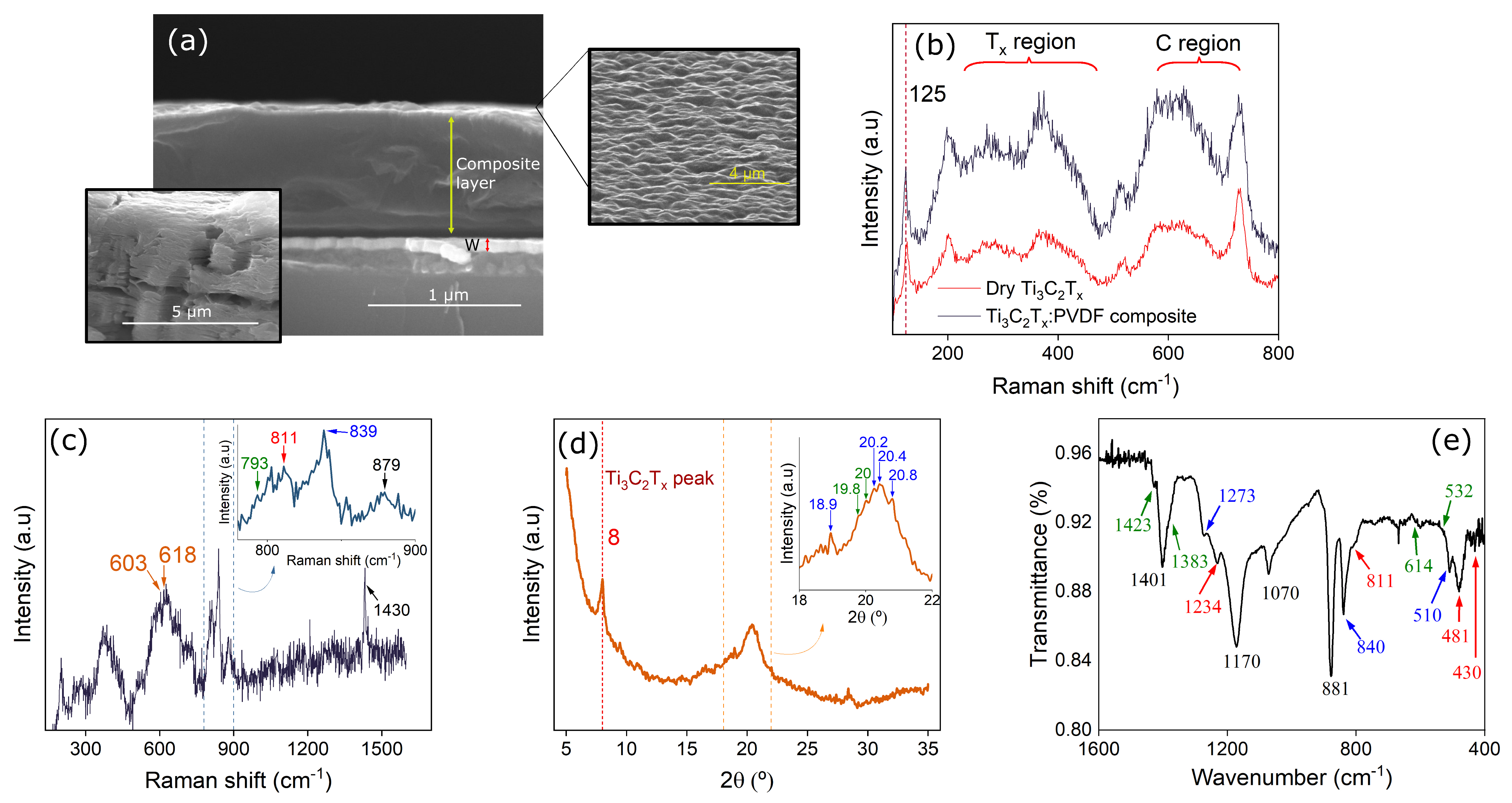
3.1. Structure Characterization

Figure 1a shows a cross section SEM image of a W/Ti3C2Tx:PVDF/Ag structure, cut by freeze-drying. A thickness of approximately 0.8 μm is visible, together with a rough surface, supported by the inset on the right, that reveals the surface of the composite. The inset on the left shows a SEM image of Ti3C2Tx flakes, dried in a metallic surface, that clearly reveals the flakes multi-layer structure.
Figure 1b shows the spectra of dry MXene flakes measured 1 day after fabrication (red curve) with the 785 nm laser. Marked by curly brackets are the regions between 230–470 cm 1 , assigned to the in-plane (Eg) vibrations of the Tx layers, and 580–730 cm 1 , assigned to both Eg and E 1 g carbon vibrations. MXenes tend to oxidize quite easily in contact with air, which represents a major disadvantage, since their electrical properties vary with the oxidation level. Therefore, we also studied the oxidation of the fabricated Ti3C2Tx MXene flakes embedded in the PVDF matrix, by measuring the spectra of the MXene composite 10 months after fabrication and exposure to ambient temperature and humidity conditions, also represented in Figure 1b (blue curve). It is clear that all the characteristic bands remain visible in the composite, and the 125 cm 1 resonance peak of MXenes is also observed. These results confirm the successful incorporation of MXenes in the PVDF polymer. Using the 633 nm laser to measure the composite, the MXenes naturally present a different characteristic spectra [Figure 1c], which can be useful to reveal their level of oxidation. The spectra shows the delaminated MXene [38] peak at 603 nm 1 , and no formation of TiO2, since this would be revealed by the appearance of a peak near 154 cm 1 , associated to the Eg mode of the TiO2 anatase phase. Only a slight red shift in the 620 nm 1 peak associated with oxidation [38] is observed. Furthermore, if considerable oxidation had occurred, the spectral region between 1000 and 1600 cm 1 should also become sizable compared to the other regions, which is not the case. We can thus conclude that, embedded in the PVDF matrix, there is no relevant oxidation of the MXene flakes after 10 months of fabrication. PVDF related bands are also visible [Figure 1c], being the 700–1400 cm 1 region the most relevant. In particular, the peak 793 cm 1 corresponds to the α phase, the peak at 839 cm 1 corresponds to the PVDF β phase, and the 811 cm 1 peak is associated to the γ phase. Peaks 879 and 1430 cm 1 are associated to the existence of the three phases.
Figure 1d shows the X-ray diffractogram of the composite thin film. The peak at 8° corresponds to Ti3C2Tx, indicating that the MXenes are delaminated. The remaining sharp peaks correspond to the crystalline phases of PVDF, while the broader bands are an indication of its amorphous phase. We see the existence of at least two phases, being α at 2 θ = 19.8, 20.0°; β at 2 θ = 18.9, 20.2, 20.4, 20.8°. γ -phase peaks are not really visible, probably due to being hidden by close α and β peaks.
Figure 1e shows the FTIR measured absorption bands of the Ti3C2Tx:PVDF film, as the crystalline phases of the PVDF can be further characterized by the infrared absorption bands comprised between 1500 and 400 cm 1 . The peaks at 881, 1070, 1170 and 1401 cm 1 that commonly appear in all three phases are visible [39]. Peaks that are usually exclusively attributed to each of the three phases are also visible, being 532, 614, 1383, and 1424 cm 1 attributable to the α phase; 510, 840 and 1273 cm 1 to the β phase; and 430, 481, 811 and 1234 cm 1 to the γ phase. So, the three common phases of PVDF are present in the thin film. For the MXenes, there is no clear peak associated to their presence, as the main characteristic peaks coincide with the range of the PVDF major bands.

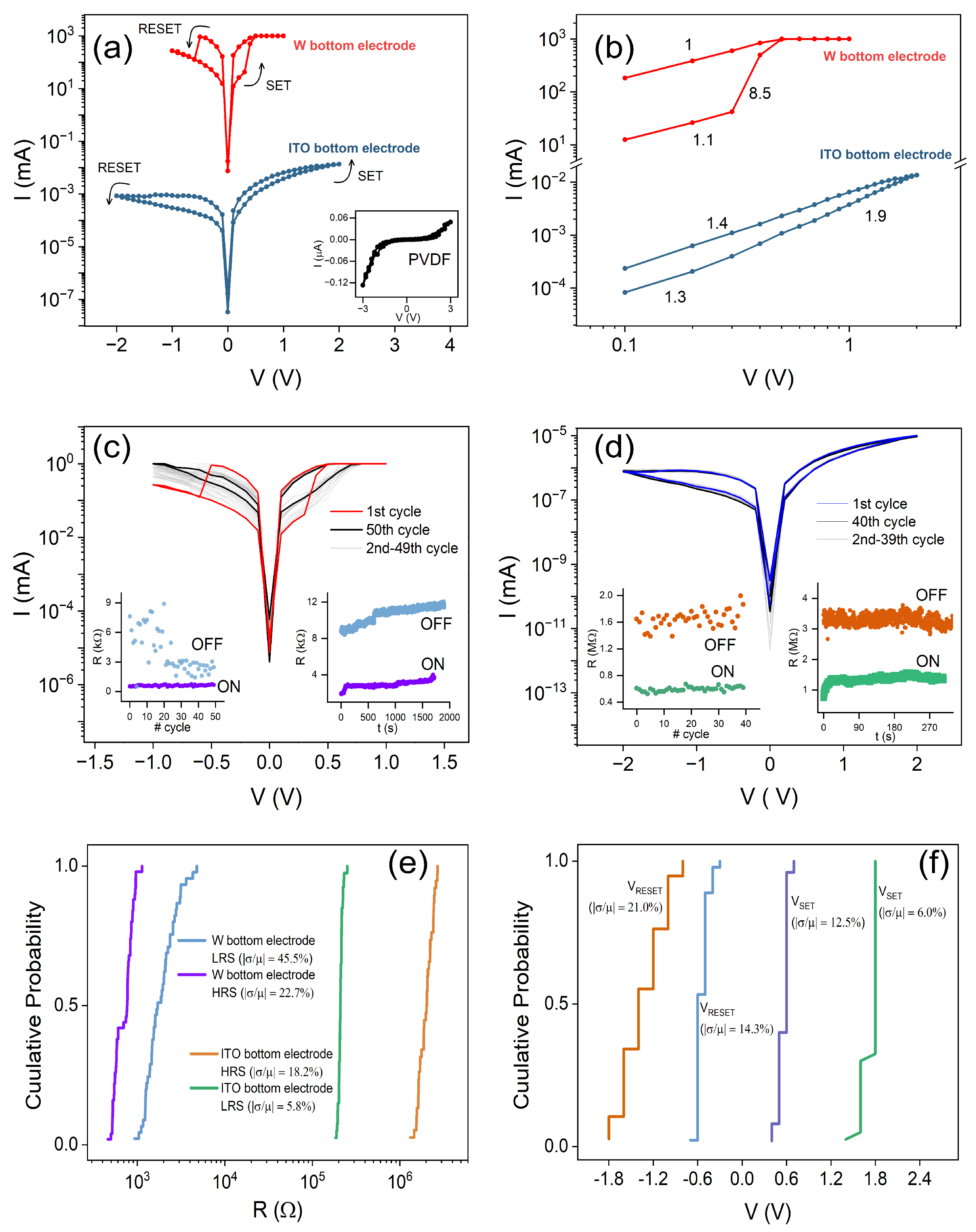
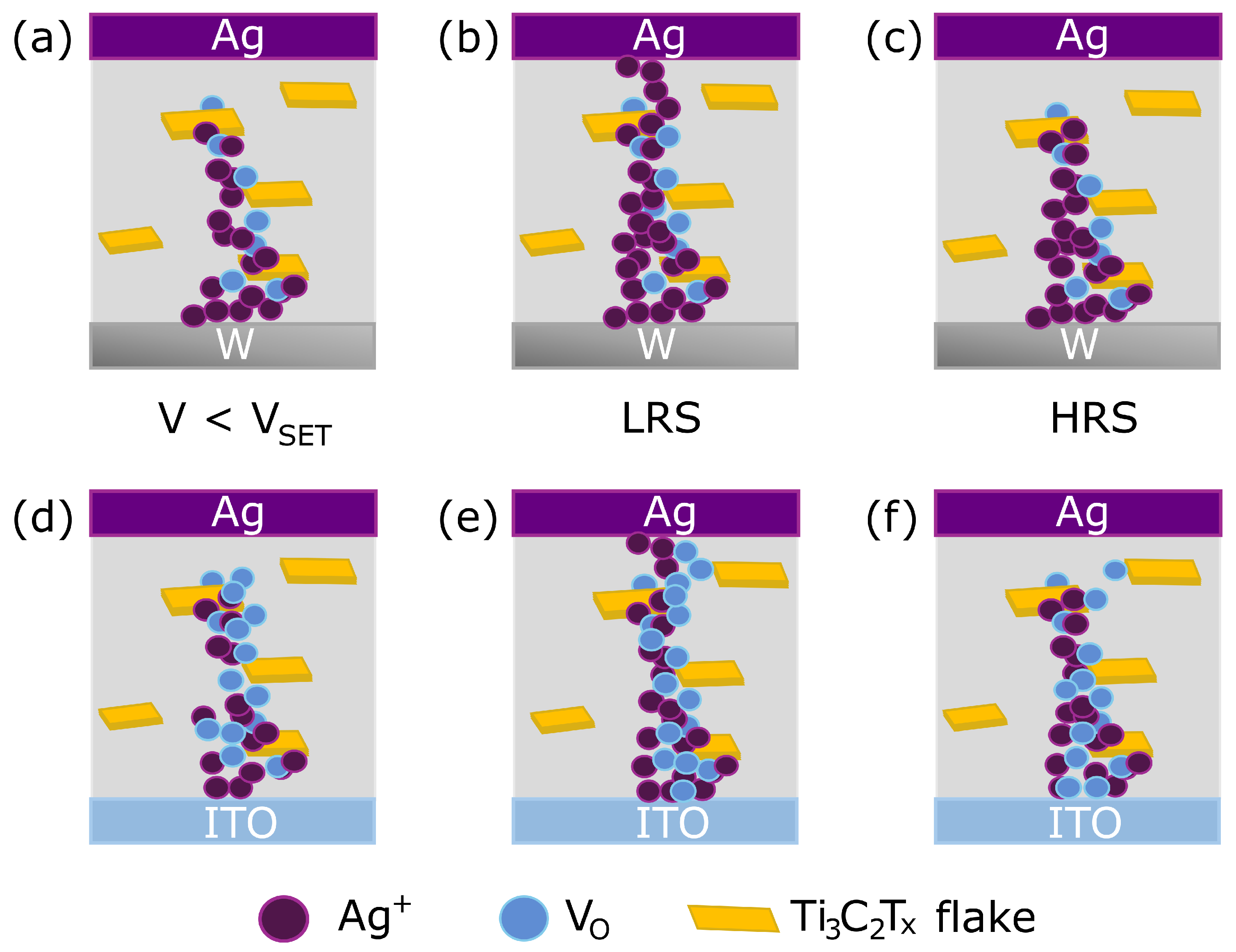
3.2. Electrical Characterization

To study the effects of MXenes and electrode material on resistive switching, we fabricated W/Ti3C2Tx:PVDF/Ag and ITO/Ti3C2Tx:PVDF/Ag structures. The measured experimental I-V curves are represented in Figure 2a, revealing bipolar resistive switching for both W and ITO bottom electrodes. It is interesting to note that, from what has been observed, no electroforming process is required to obtain switching behaviour. In the W/Ti3C2Tx:PVDF/Ag structure (red curve), the initial resistance is about 8 k Ω , and switching from low to high conductance (SET process) occurs at a bias of ≈0.3 V, reaching the current compliance of 1 mA, with a minimum resistance of 540 Ω , giving a ON/OFF ratio of 15. By sweeping the voltage to negative values, the high resistance state is recovered (RESET process) at −0.5 V. The characteristic RS curve of the ITO/Ti3C2Tx:PVDF/Ag structure (blue curve) exhibits a much more gradual HRS to LRS transition, with no well defined V S E T or V R E S E T . The initial resistance is 1.2 M Ω , with SET process at positive bias leading to a resistance of 430 k Ω , giving an ON/OFF ratio of 3. Furthermore, the hysteresis is less pronounced, appearing more collapsed. The HRS is obtained by sweeping to negative voltage values (RESET process), also more gradually. As a control, we fabricated W/PVDF/Ag, with no MXenes. The inset of Figure 2a shows the corresponding I−V behaviour, clearly demonstrating the absence of hysteresis in the curve, with a initial resistance of approximately 500 M Ω . This indicates the critical role of the MXenes for the observation of resistive switching.
To explore the conduction mechanisms present in these structures, the I−V curves are represented in logarithmic scale in Figure 2b. For the W-based structure, the slope of the curve at low voltage is 1.1, showing a close to linear relation (I ∝ V) similar to the ohmic conduction model. As voltage increases, a sudden slope enhancement to 8.5 is observed near the SET voltage, indicating an abrupt increase in current. The structure then turns into the LRS, meaning that all the traps in the active layer are filled and the movement of free charges is enabled, increasing the current. By this stage, the curve has a slope of 1, indicating ohmic conduction. Concerning the ITO-based structure, the low voltage region between 0 and 0.3 V presents a slope of 1.3. In the 0.3 to 2 V range, the slope increases to 1.9. This is in agreement with the Child conduction mechanism (I ∝ V 2 ), during which the injection of more carriers is limited by the space charge of the active layer. As the voltage is swept back to zero, the slope is 1.4. By these analyses, we can attribute the conduction of the structure in the HRS to trap-filled space charge limited conduction (SCLC). Comparing the two curves in Figure 2b, it is clear that the ITO-based structure shows a much more gradual switching to the LRS.
Figure 2c,d show the cyclability, endurance, and HRS/LRS retention of the W and ITO-based structures, respectively. The W/Ti3C2Tx:PVDF/Ag structure shows an endurance of over 50 cycles and a retention larger than 30 min. Concerning cycling, we see that the OFF resistance tends to gradually decrease after multiple cycles. The ITO/Ti3C2Tx:PVDF/Ag structure shows an endurance of at least 40 cycles, with constant ON and OFF resistances. Concerning retention, the ON state has been kept for at least 5 min. The cumulative probability distribution confirms the small variability of the LRS for both structures [Figure 2e], and lower in general for the ITO bottom electrode structure. Concerning the cumulative probability for SET and RESET voltages [Figure 2f], it shows basically the same variability for SET and RESET with the W bottom electrode, and minimum for SET with ITO, while maximum for RESET.
The resistive switching behaviours we obtained are influenced by both top active electrode and the presence of oxygen vacancy terminations in the MXene flakes, which also serve as nucleation centres, creating an interplay between the Ag+ ions and oxygen vacancies, as represented in Figure 3a–f, for W/Ti3C2Tx:PVDF/Ag and ITO/Ti3C2Tx:PVDF/Ag, respectively. This is the main difference from the single PVDF layer that did not show resistive switching. Concerning the top electrode effect, as voltage is increased, Ag atoms are oxidized, forming Ag+ ions that migrate towards the bottom electrode, eventually forming a filament that allows the free flow of charges in the LRS, leading to ohmic conduction. The MXene flakes serve as trapping sites in the dielectric layer that allow the nucleation of ions. Furthermore, the application of an electric field also creates oxygen vacancy movement that will drift and try to form a filament of vacancies, creating two competing mechanisms.
In fact, as seen above, the ITO-based structure displays a softer transition into LRS, indicating the relevance of oxygen vacancies role, in competition with the Ag filament formation. This is probably due to the ITO layer serving as an oxygen reservoir that feeds this competing mechanism and leads to a less pronounced switching.

4. Conclusions

In summary, conductive filament-based resistive switching is demonstrated in Ti3C2Tx:PVDF composites, revealing the crucial role of MXenes to enable this effect. Furthermore, PVDF improves the stability of the MXene flakes, which show no oxidation up to 10 months after fabrication. Both structures show bipolar non-volatile switching behaviour, being the ITO-based structure more stable during sweeping cycles, but presenting shorter retention of the ON state than the W-based one. Thus, further investigation of these structures taking advantage of the flexible PET/ITO substrate should be considered. The conduction mechanism in the active layer is governed by the space charge limited conduction in the HRS, trap-charge limited as V S E T is reached and ohmic conduction processes in the LRS. We consider that this originates from an interplay of both top active electrode and the MXene flakes serving as nucleation centres for Ag+ ions, as well as containing oxygen vacancies terminations, creating a competing mechanism which is more pronounced in the ITO-based structure. To support this, further measurements using in situ electrical or element mapping measurements should be performed. Our analysis provides a further understating of RS devices and performance based on MXenes integration with polymers and different electrode structures, a fundamental step towards their use in this technology.

Author Contributions

Conceptualization, M.G. and C.D. and J.V.; methodology, M.G. and H.T.; software, H.T. and J.V.; validation, C.D. and J.V.; formal analysis, M.G.; investigation, M.G. and H.T.; resources, C.D. and J.V.; data curation, M.G.; writing—original draft preparation, M.G.; writing—review and editing, M.G., C.D. and J.V.; visualization, M.G.; supervision, C.D. and J.V.; project administration, C.D. and J.V.; funding acquisition, C.D. and J.V. All authors have read and agreed to the published version of the manuscript.

Funding

This work was financially supported by FEDER through COMPETE2020—Programa Operacional Competitividade e Internacionalização (POCI) and by FCT through projects PTDC/NANMAT/4093/2021 and 2022.15710.UTA, and Foundation ‘la Caixa’—Caixa Research Health 2022 (grant HR22-00189). The authors also acknowledge Projects UIDB/04968/2025 and UIDP/04968/2025, financed by national funds through FCT/MCTES (PIDDAC).

Institutional Review Board Statement

Not applicable.

Data Availability Statement

The raw data supporting the conclusions of this article will be made available by the authors on request.

Conflicts of Interest

The authors declare no conflicts of interest.

Abbreviations

The following abbreviations are used in this manuscript:
2DTwo-Dimensional
FTIRFourier-Transform Infrared Spectroscopy
HRSHigh resistance state
LRSLow resistance state
MIMMetal-Insulator-Metal
RSResistive switching
SCLCSpace Charge Limited Conduction
SEMScanning Electron Microscopy
XRDX-ray Diffraction

References

  1. Chua, L. Memristor—The missing circuit element. IEEE Trans. Circuit Theory 1971, 18, 507–519. [Google Scholar] [CrossRef]
  2. Strukov, D.B.; Snider, G.S.; Stewart, D.R.; Williams, R.S. The missing memristor found. Nature 2008, 453, 80–83. [Google Scholar] [CrossRef] [PubMed]
  3. Dias, C.; Castro, D.; Aroso, M.; Ventura, J.; Aguiar, P. Memristor-Based Neuromodulation Device for Real-Time Monitoring and Adaptive Control of Neuronal Populations. ACS Appl. Electron. Mater. 2022, 4, 2380–2387. [Google Scholar] [CrossRef] [PubMed]
  4. Waser, R.; Dittmann, R.; Staikov, G.; Szot, K. Redox-Based Resistive Switching Memories—Nanoionic Mechanisms, Prospects, and Challenges. Adv. Mater. 2009, 21, 2632–2663. [Google Scholar] [CrossRef]
  5. Yang, J.J.; Strukov, D.B.; Stewart, D.R. Memristive devices for computing. Nat. Nanotechnol. 2013, 8, 13–24. [Google Scholar] [CrossRef]
  6. Liu, L.; Xiong, W.; Liu, Y.; Chen, K.; Xu, Z.; Zhou, Y.; Han, J.; Ye, C.; Chen, X.; Song, Z.; et al. Designing High-Performance Storage in HfO2/BiFeO3 Memristor for Artificial Synapse Applications. Adv. Electron. Mater. 2020, 6, 1901012. [Google Scholar] [CrossRef]
  7. Zhang, H.; Jiang, B.; Cheng, C.; Huang, B.; Zhang, H.; Chen, R.; Xu, J.; Huang, Y.; Chen, H.; Pei, W.; et al. A Self-Rectifying Synaptic Memristor Array with Ultrahigh Weight Potentiation Linearity for a Self-Organizing-Map Neural Network. Nano Lett. 2023, 23, 3107–3115. [Google Scholar] [CrossRef]
  8. Patnaik, A.; Acharya, A.; Tiwari, K.; Saha, P.; Sahoo, N.; Panda, D. Synaptic plasticity in zinc oxide-based flexible invisible transparent memristor by modulating oxygen concentration. J. Appl. Phys. 2024, 136, 045109. [Google Scholar] [CrossRef]
  9. Yang, J.; Zhang, F.; Xiao, H.M.; Wang, Z.P.; Xie, P.; Feng, Z.; Wang, J.; Mao, J.; Zhou, Y.; Han, S.T. A Perovskite Memristor with Large Dynamic Space for Analog-Encoded Image Recognition. ACS Nano 2022, 16, 21324–21333. [Google Scholar] [CrossRef]
  10. Patel, M.; Kumbhar, D.D.; Gosai, J.; Sekhar, M.R.; Mallajosyula, A.T.; Solanki, A. Hybrid Perovskite-Based Flexible and Stable Memristor by Complete Solution Process for Neuromorphic Computing. Adv. Electron. Mater. 2023, 9, 2200908. [Google Scholar] [CrossRef]
  11. Cao, F.; Hu, Z.; Yan, T.; Hong, E.; Deng, X.; Wu, L.; Fang, X. A Dual-Functional Perovskite-Based Photodetector and Memristor for Visual Memory. Adv. Mater. 2023, 35, 2304550. [Google Scholar] [CrossRef] [PubMed]
  12. Cao, G.; Meng, P.; Chen, J.; Liu, H.; Bian, R.; Zhu, C.; Liu, F.; Liu, Z. 2D Material Based Synaptic Devices for Neuromorphic Computing. Adv. Funct. Mater. 2021, 31, 2005443. [Google Scholar] [CrossRef]
  13. Duan, H.; Cheng, S.; Qin, L.; Zhang, X.; Xie, B.; Zhang, Y.; Jie, W. Low-Power Memristor Based on Two-Dimensional Materials. J. Phys. Chem. Lett. 2022, 13, 7130–7138. [Google Scholar] [CrossRef] [PubMed]
  14. Nirmal, K.A.; Kumbhar, D.D.; Kesavan, A.V.; Dongale, T.D.; Kim, T.G. Advancements in 2D layered material memristors: Unleashing their potential beyond memory. NPJ 2D Mater. Appl. 2024, 8, 83. [Google Scholar] [CrossRef]
  15. Rehman, M.M.; Samad, Y.A.; Gul, J.Z.; Saqib, M.; Khan, M.; Shaukat, R.A.; Chang, R.; Shi, Y.; Kim, W.Y. 2D materials-memristive devices nexus: From status quo to Impending applications. Prog. Mater. Sci. 2025, 152, 101471. [Google Scholar] [CrossRef]
  16. Teja Nibhanupudi, S.S.; Roy, A.; Veksler, D.; Coupin, M.; Matthews, K.C.; Disiena, M.; Ansh; Singh, J.V.; Gearba-Dolocan, I.R.; Warner, J.; et al. Ultra-fast switching memristors based on two-dimensional materials. Nat. Commun. 2024, 15, 2334. [Google Scholar] [CrossRef]
  17. Ares, P.; Novoselov, K.S. Recent advances in graphene and other 2D materials. Nano Mater. Sci. 2022, 4, 3–9. [Google Scholar] [CrossRef]
  18. An, J.; Zhao, X.; Zhang, Y.; Liu, M.; Yuan, J.; Sun, X.; Zhang, Z.; Wang, B.; Li, S.; Li, D. Perspectives of 2D Materials for Optoelectronic Integration. Adv. Funct. Mater. 2022, 32, 2110119. [Google Scholar] [CrossRef]
  19. Zhang, X.; Chen, H.; Cheng, S.; Guo, F.; Jie, W.; Hao, J. Tunable Resistive Switching in 2D MXene Ti3C2 Nanosheets for Non-Volatile Memory and Neuromorphic Computing. ACS Appl. Mater. Interfaces 2022, 14, 44614–44621. [Google Scholar] [CrossRef]
  20. Yan, X.; Wang, K.; Zhao, J.; Zhou, Z.; Wang, H.; Wang, J.; Zhang, L.; Li, X.; Xiao, Z.; Zhao, Q.; et al. A New Memristor with 2D Ti3C2Tx MXene Flakes as an Artificial Bio-Synapse. Small 2019, 15, 1900107. [Google Scholar] [CrossRef]
  21. Ling, S.; Zhang, C.; Ma, C.; Li, Y.; Zhang, Q. Emerging MXene-Based Memristors for In-Memory, Neuromorphic Computing, and Logic Operation. Adv. Funct. Mater. 2023, 33, 2208320. [Google Scholar] [CrossRef]
  22. Teixeira, H.; Dias, C.; Silva, A.V.; Ventura, J. Advances on MXene-Based Memristors for Neuromorphic Computing: A Review on Synthesis, Mechanisms, and Future Directions. ACS Nano 2024, 18, 21685–21713. [Google Scholar] [CrossRef] [PubMed]
  23. Gogotsi, Y.; Anasori, B. The Rise of MXenes. ACS Nano 2019, 13, 8491–8494. [Google Scholar] [CrossRef] [PubMed]
  24. Hart, J.L.; Hantanasirisakul, K.; Lang, A.C.; Anasori, B.; Pinto, D.; Pivak, Y.; Van Omme, J.T.; May, S.J.; Gogotsi, Y.; Taheri, M.L. Control of MXenes’ electronic properties through termination and intercalation. Nat. Commun. 2019, 10, 522. [Google Scholar] [CrossRef]
  25. Ahmad, S.; Ashraf, I.; Mansoor, M.A.; Rizwan, S.; Iqbal, M. An Overview of Recent Advances in the Synthesis and Applications of the Transition Metal Carbide Nanomaterials. Nanomaterials 2021, 11, 776. [Google Scholar] [CrossRef]
  26. Gong, Y.; Xing, X.; Wang, Y.; Lv, Z.; Zhou, Y.; Han, S.T. Emerging MXenes for Functional Memories. Small Sci. 2021, 1, 2100006. [Google Scholar] [CrossRef]
  27. Jiang, X.; Kuklin, A.V.; Baev, A.; Ge, Y.; Ågren, H.; Zhang, H.; Prasad, P.N. Two-dimensional MXenes: From morphological to optical, electric, and magnetic properties and applications. Phys. Rep. 2020, 848, 1–58. [Google Scholar] [CrossRef]
  28. Muhammed, M.; Mokkath, J. Surface termination dependent optical characteristics of MXene nanoflakes. Mater. Today Chem. 2023, 29, 101447. [Google Scholar] [CrossRef]
  29. Tang, M.; Li, J.; Wang, Y.; Han, W.; Xu, S.; Lu, M.; Zhang, W.; Li, H. Surface Terminations of MXene: Synthesis, Characterization, and Properties. Symmetry 2022, 14, 2232. [Google Scholar] [CrossRef]
  30. Lian, X.J.; Fu, J.K.; Gao, Z.X.; Gu, S.P.; Wang, L. High-performance artificial neurons based on Ag/MXene/GST/Pt threshold switching memristors. Chin. Phys. B 2023, 32, 017304. [Google Scholar] [CrossRef]
  31. Mao, H.; Gu, C.; Yan, S.; Xin, Q.; Cheng, S.; Tan, P.; Wang, X.; Xiu, F.; Liu, X.; Liu, J.; et al. MXene Quantum Dot/Polymer Hybrid Structures with Tunable Electrical Conductance and Resistive Switching for Nonvolatile Memory Devices. Adv. Electron. Mater. 2020, 6, 1900493. [Google Scholar] [CrossRef]
  32. Sang, M.; Liu, S.; Li, W.; Wang, S.; Li, J.; Li, J.; Xuan, S.; Gong, X. Flexible polyvinylidene fluoride(PVDF)/MXene(Ti3C2Tx)/Polyimide(PI) wearable electronic for body Monitoring, thermotherapy and electromagnetic interference shielding. Compos. Part A Appl. Sci. Manuf. 2022, 153, 106727. [Google Scholar] [CrossRef]
  33. Qin, Q.; Hu, Y.; Guo, S.; Yang, Y.; Lei, T.; Cui, Z.; Wang, H.; Qin, S. PVDF-based composites for electromagnetic shielding application: A review. J. Polym. Res. 2023, 30, 130. [Google Scholar] [CrossRef]
  34. Wang, Y.; Guo, T.; Tian, Z.; Bibi, K.; Zhang, Y.Z.; Alshareef, H.N. MXenes for Energy Harvesting. Adv. Mater. 2022, 34, 2108560. [Google Scholar] [CrossRef]
  35. Kou, L.; Sadri, R.; Momodu, D.; Roberts, E.P.L.; Mohammad Haniff, M.A.S.; Wu, C.; Dee, C.F.; Ooi, P.C. N -Doped Graphene/MXene Nanocomposite as a Temperature-Adaptive Neuromorphic Memristor. ACS Appl. Nano Mater. 2024, 7, 3631–3644. [Google Scholar] [CrossRef]
  36. Wu, Y.; Li, Y.; Wang, Y.; Liu, Q.; Chen, Q.; Chen, M. Advances and prospects of PVDF based polymer electrolytes. J. Energy Chem. 2022, 64, 62–84. [Google Scholar] [CrossRef]
  37. Dallaev, R.; Pisarenko, T.; Sobola, D.; Orudzhev, F.; Ramazanov, S.; Trčka, T. Brief Review of PVDF Properties and Applications Potential. Polymers 2022, 14, 4793. [Google Scholar] [CrossRef]
  38. Adomaviciute-Grabusove, S.; Popov, A.; Ramanavicius, S.; Sablinskas, V.; Shevchuk, K.; Gogotsi, O.; Baginskiy, I.; Gogotsi, Y.; Ramanavicius, A. Monitoring Ti3C2Tx MXene Degradation Pathways Using Raman Spectroscopy. ACS Nano 2024, 18, 13184–13195. [Google Scholar] [CrossRef]
  39. Cai, X.; Lei, T.; Sun, D.; Lin, L. A critical analysis of the α, β and γ phases in poly(vinylidene fluoride) using FTIR. RSC Adv. 2017, 7, 15382–15389. [Google Scholar] [CrossRef]
Figure 1. Structural characterization of the Ti3C2Tx:PVDF active layer. (a) SEM cross section image of the layer, revealing a thickness of 0.8 μm. The inset on the left shows a SEM image of the MXene flakes. The inset on the right shows the surface of the composite after deposition. (b) Comparison of the Raman spectra of dry MXene flakes and composite layer measured using the 785 nm laser. (c) Raman spectra of composite layer measured using the 633 nm laser. (d) XRD and (e) FTIR spectra of the composite layer.
Polymers 17 01309 g001
Figure 2. (a) I−V characteristics of W/Ti3C2Tx:PVDF/Ag (red) and ITO/Ti3C2Tx:PVDF/Ag (blue). The inset shows the I−V characteristic curve obtained for a W/PVDF/Ag control structure. (b) ln(I)−ln(V) characteristics of W/Ti3C2Tx:PVDF/Ag (red) and ITO/Ti3C2Tx:PVDF/Ag (blue). Cycling, endurance (left inset) and retention performance (right inset) of (c) W/Ti3C2Tx:PVDF/Ag and (d) ITO/Ti3C2Tx:PVDF/Ag. Cumulative probability of (e) resistance and (f) voltage in HRS and LRS, for both structures.
Polymers 17 01309 g002
Figure 3. Schematic representation of the conduction mechanism interplay between Ag ions and oxygen vacancies present as MXene surface terminations in the (ac) W/Ti3C2Tx:PVDF/Ag and (df) ITO/Ti3C2Tx:PVDF/Ag structures.
Polymers 17 01309 g003
Disclaimer/Publisher’s Note: The statements, opinions and data contained in all publications are solely those of the individual author(s) and contributor(s) and not of MDPI and/or the editor(s). MDPI and/or the editor(s) disclaim responsibility for any injury to people or property resulting from any ideas, methods, instructions or products referred to in the content.

