
Polymer Nanoparticles Applied in the CMP (Chemical Mechanical Polishing) Process of Chip Wafers for Defect Improvement and Polishing Removal Rate Response

Abstract
:
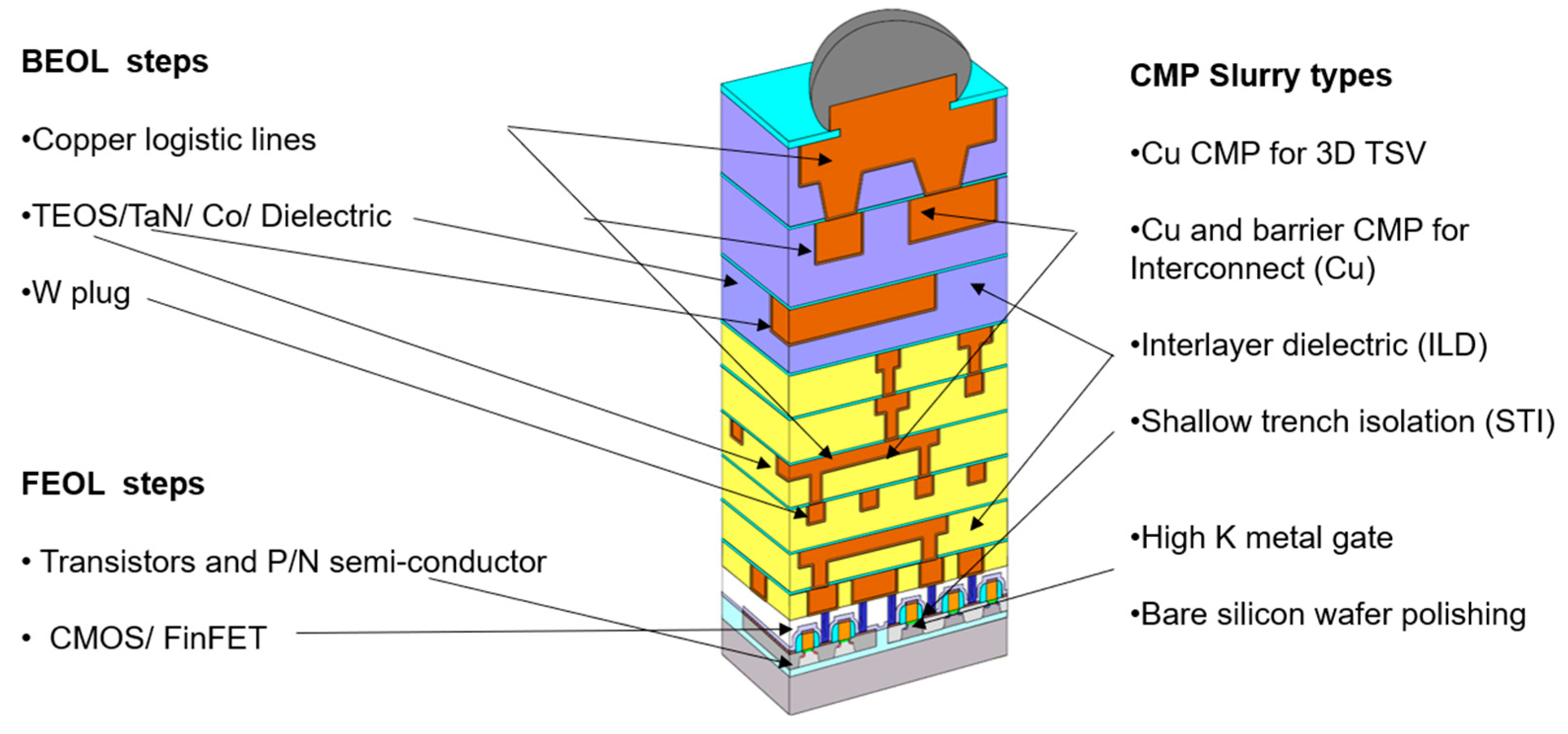
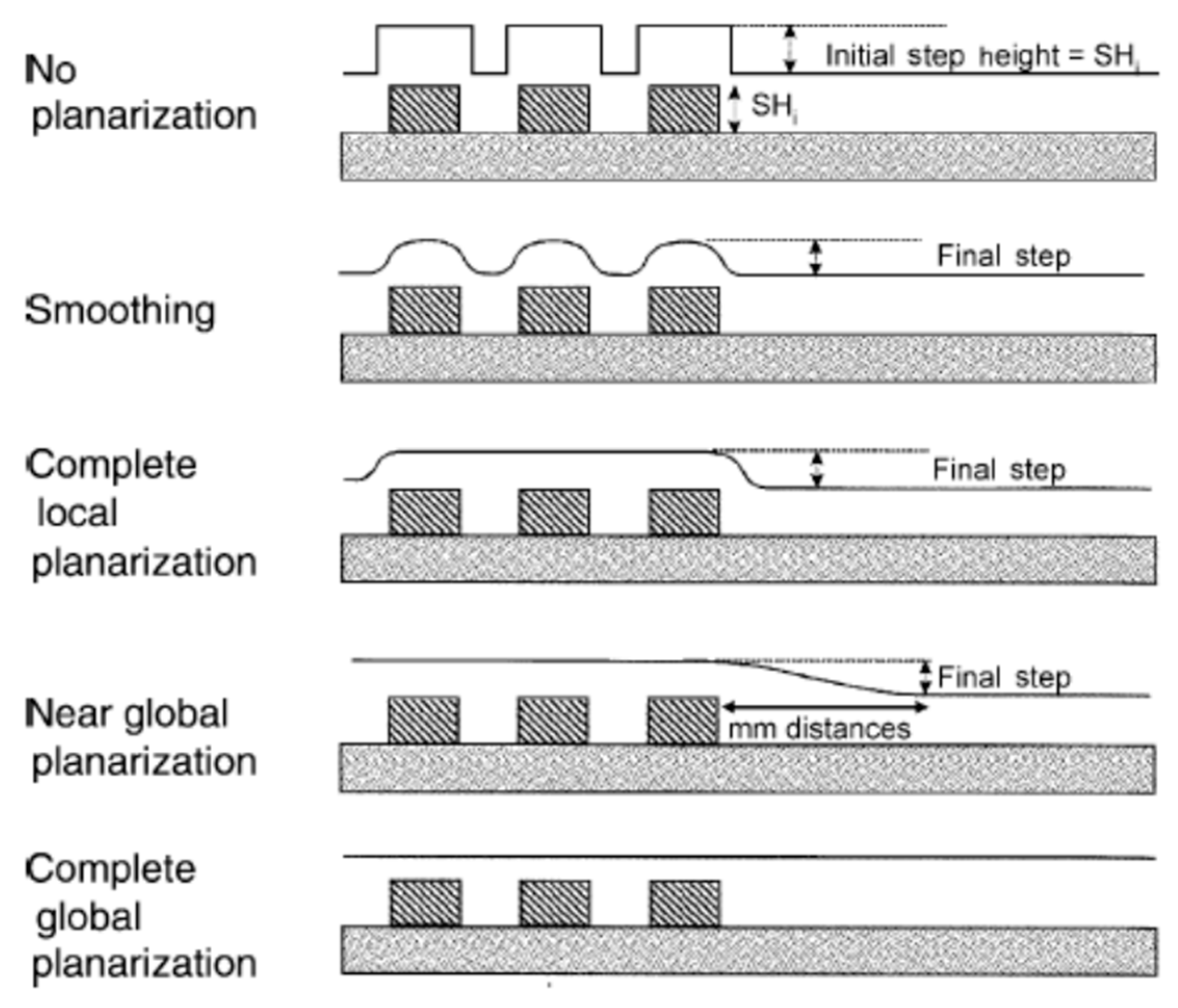
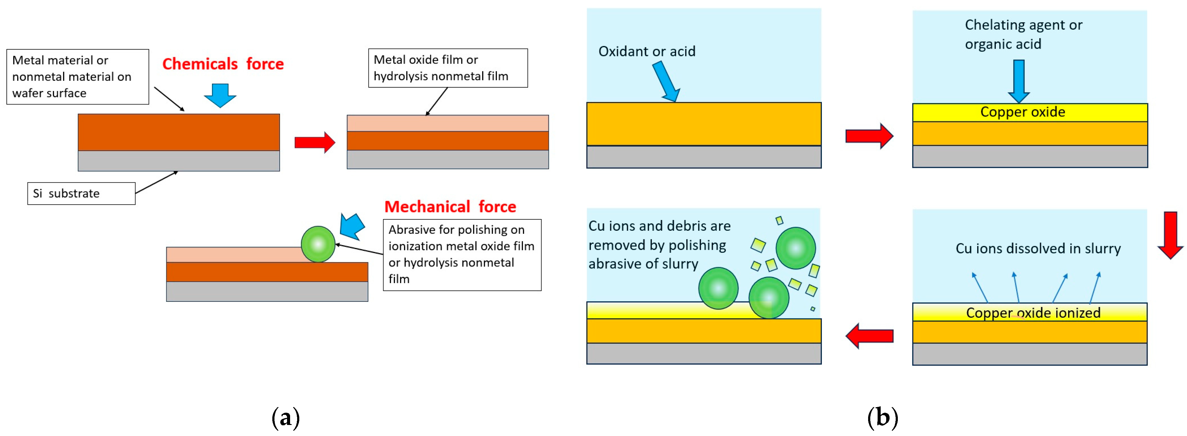
1. Introduction
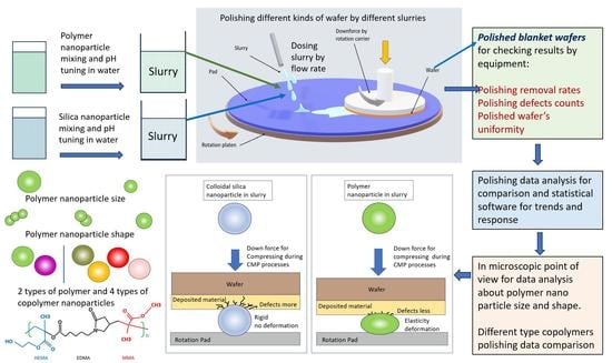
2. Materials and Methods
3. Results and Discussion
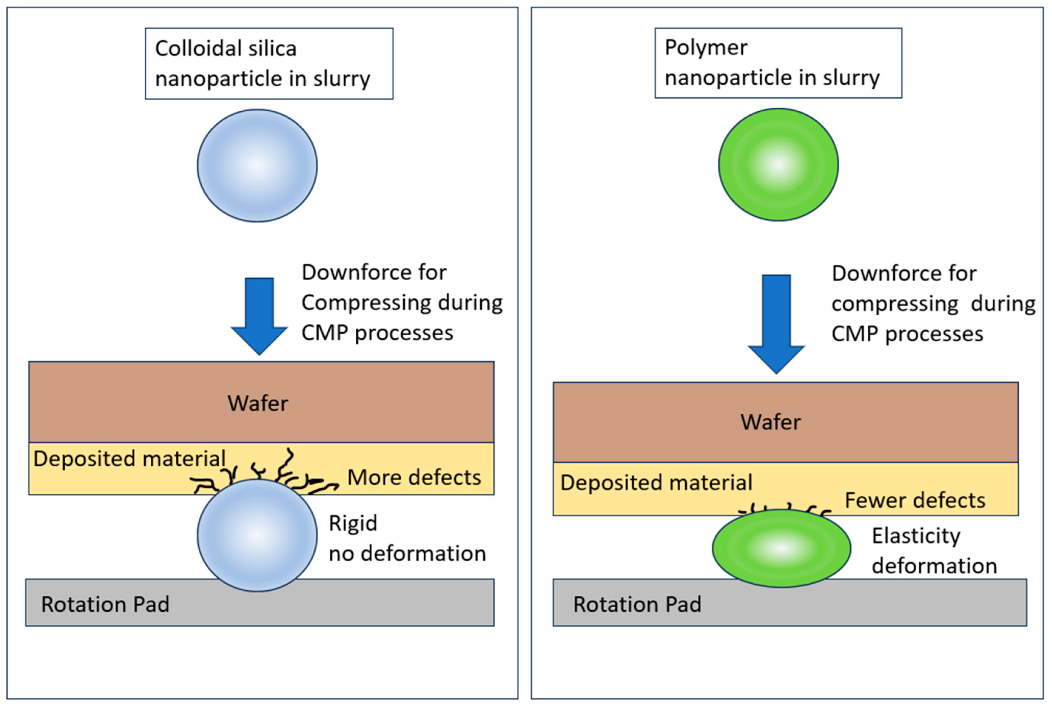
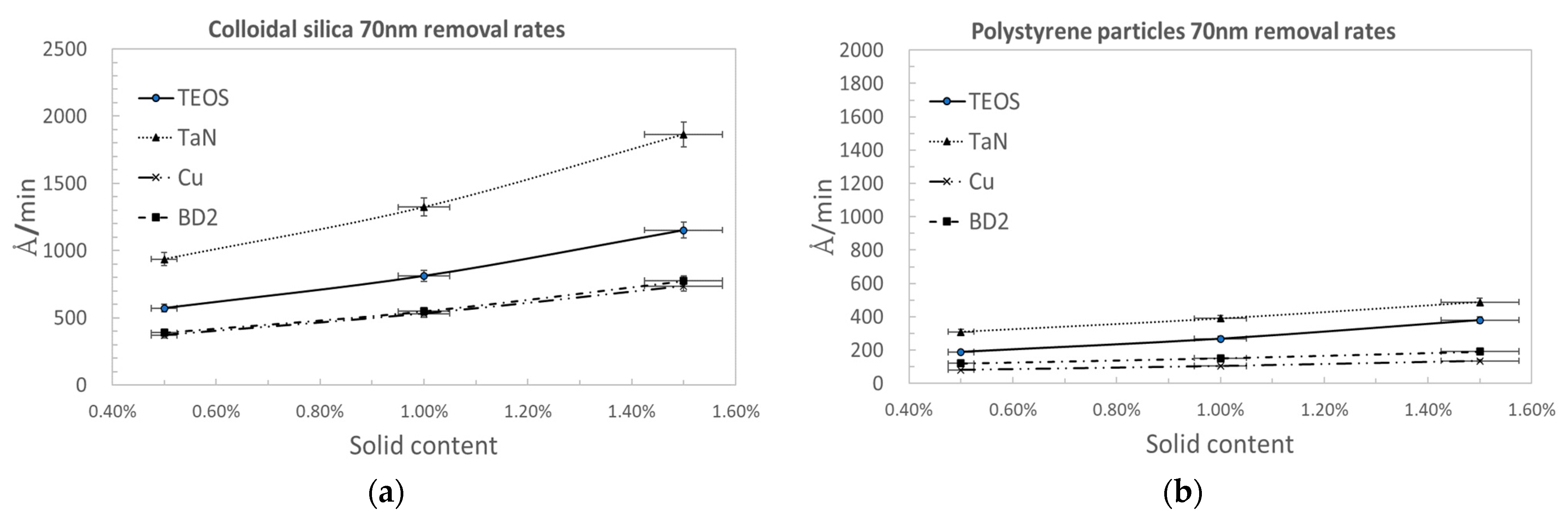
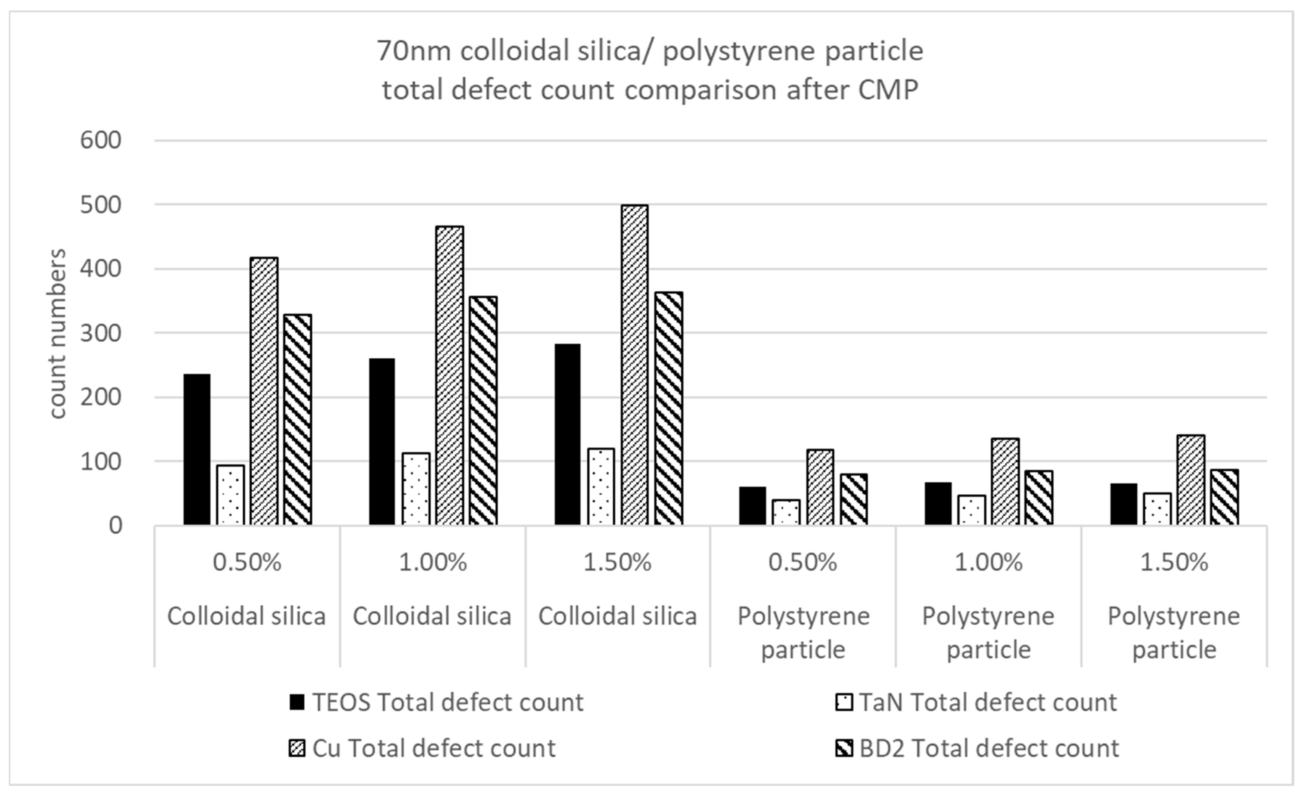
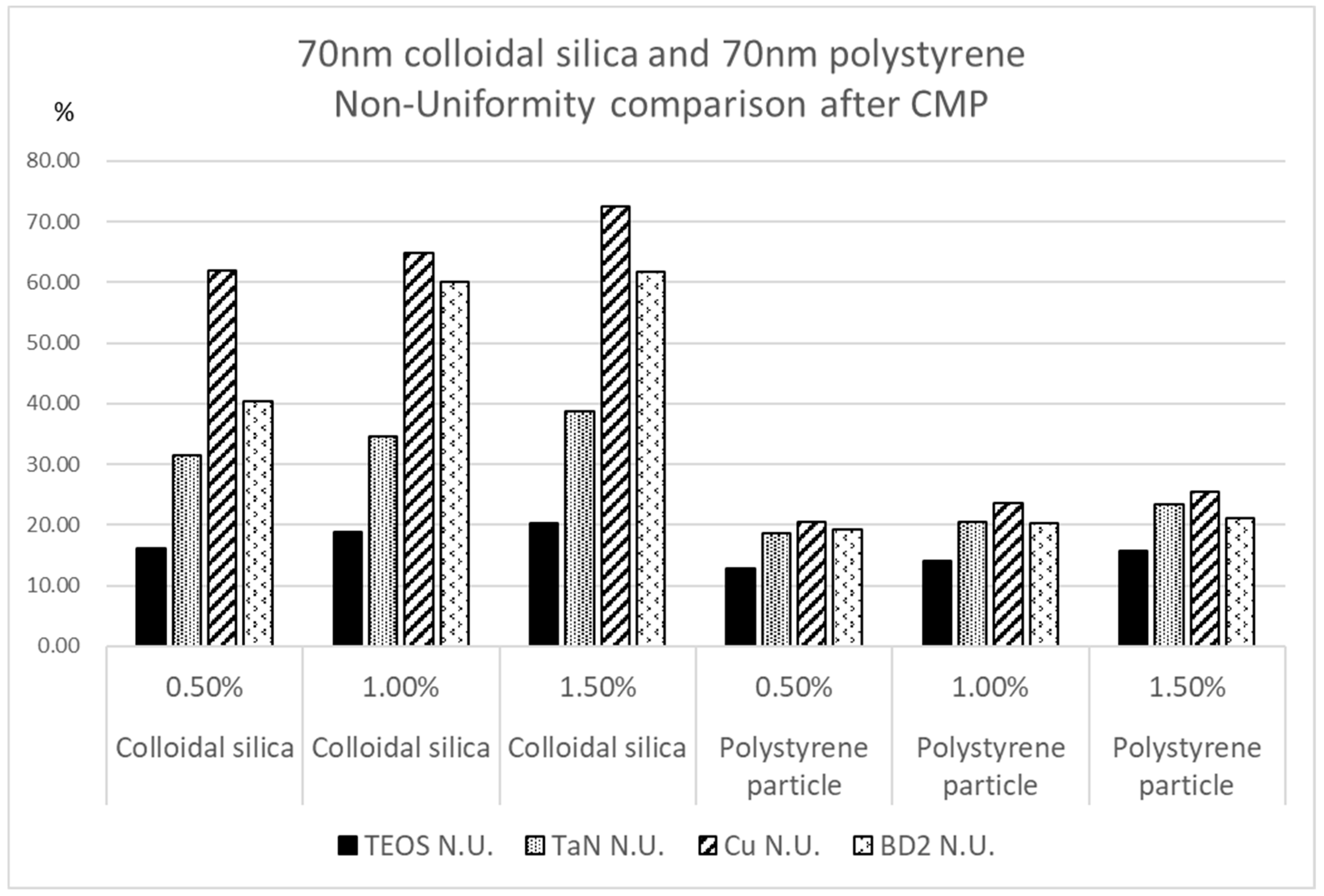
3.1. Comparison by Nanoparticle Solid Content of Traditional Silica Nanoparticles and Polymer Nanoparticles for CMP Polishing Performance
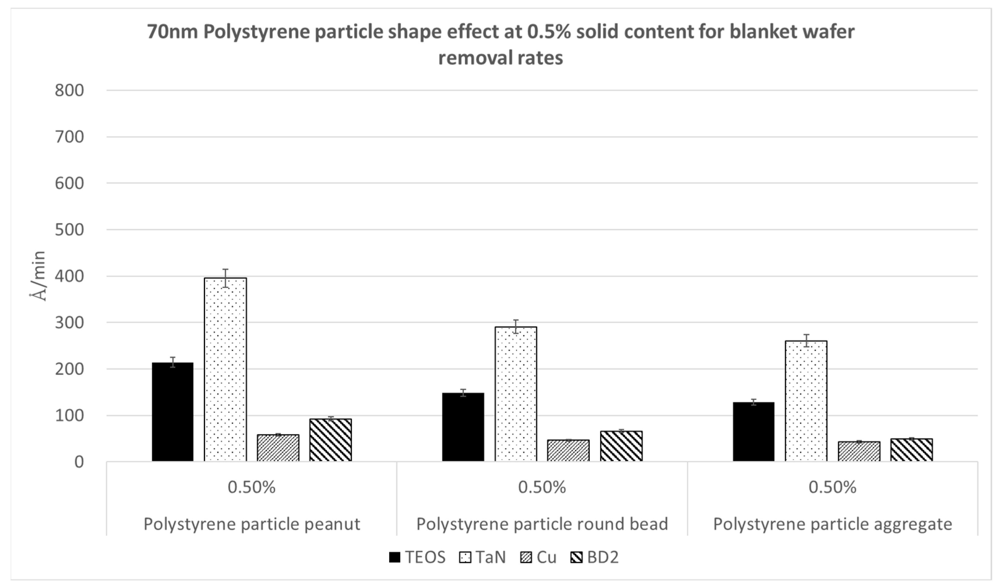
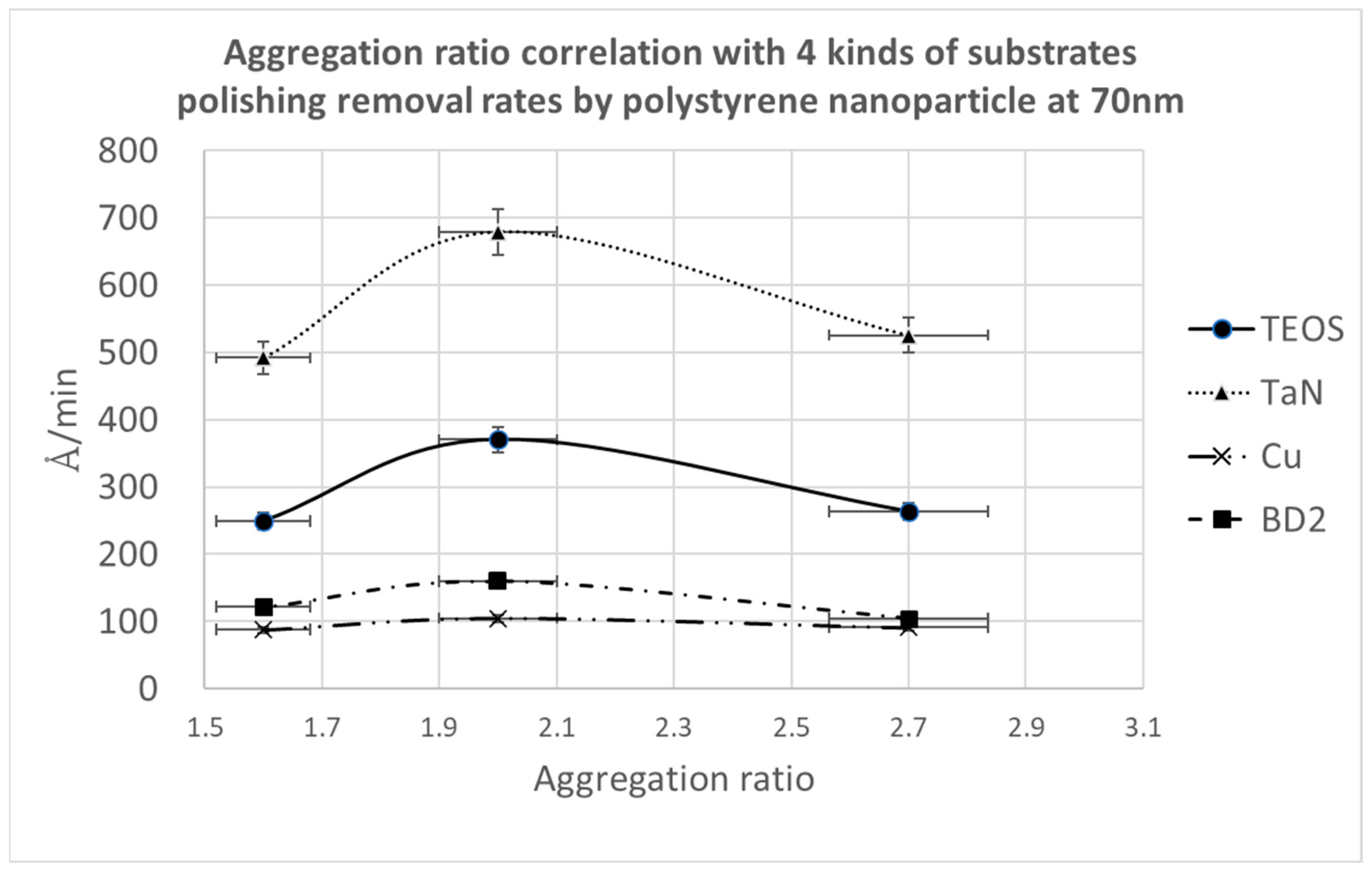
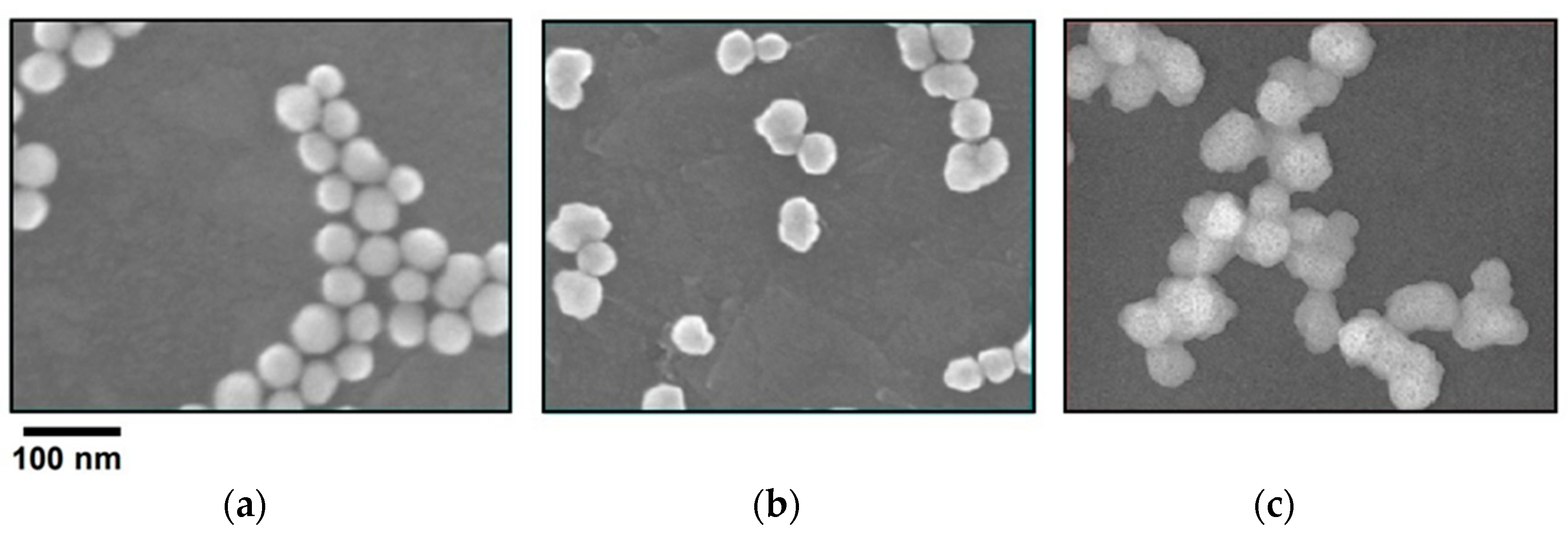
3.2. Effect of Polishing Particle Shape
3.3. Polymer Nanoparticle Size Effect
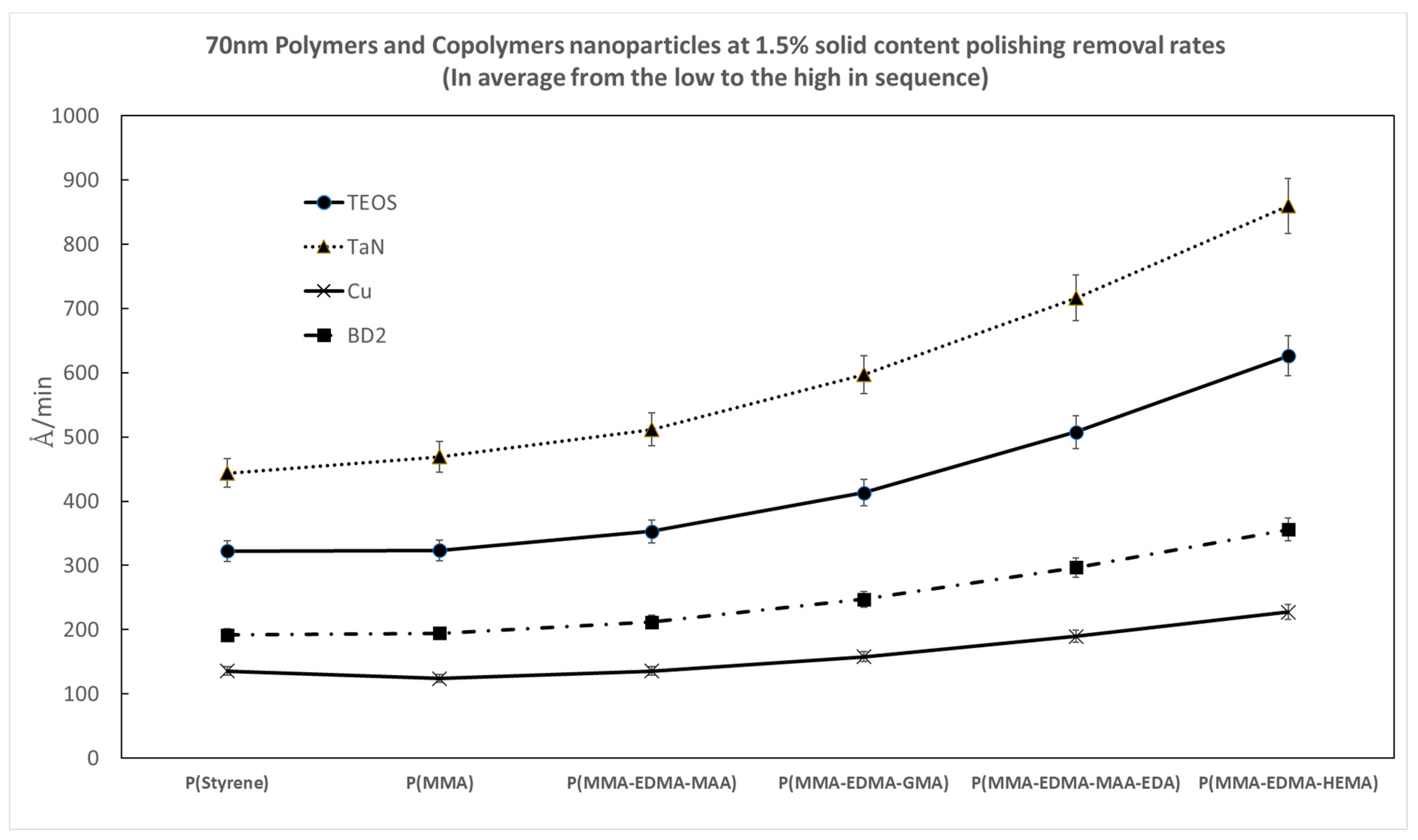
3.4. Effects of Various Copolymer Nanoparticle Molecules on CMP Polishing Performance
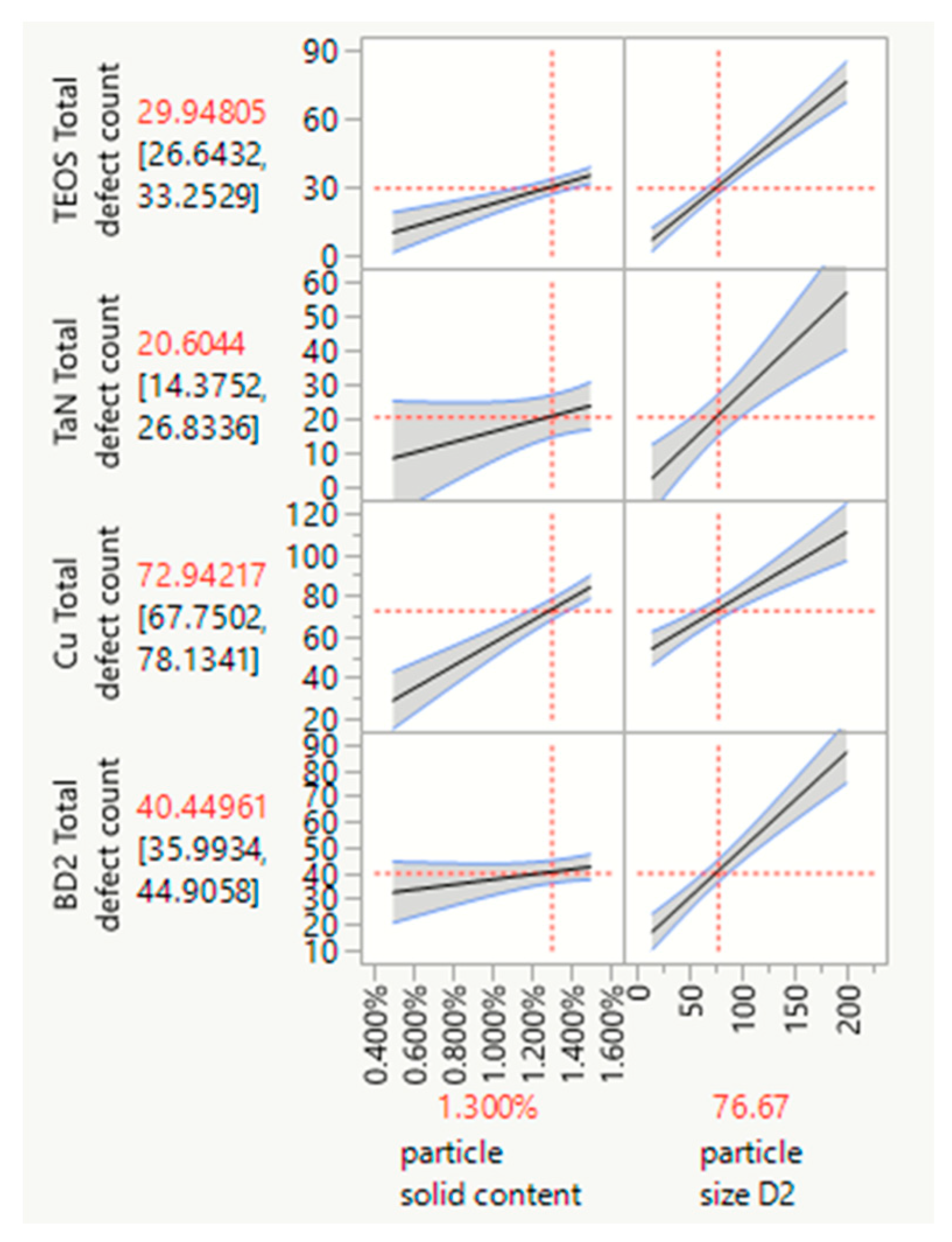
3.5. JMP® (SAS Institute) Statistic Software Analysis of the Polishing Data of Polymer Nanoparticles
3.6. A Comparison of Pattern Wafer Polishing Results between Colloidal Silica and Polymer Nanoparticles
4. Conclusions
Author Contributions
Funding
Institutional Review Board Statement
Data Availability Statement
Acknowledgments
Conflicts of Interest
References
- Park, Y.; Jeong, H.; Choi, S.; Jeong, H. Planarization of Wafer Edge Profile in Chemical Mechanical Polishing. Int. J. Precis. Eng. Manuf. 2013, 14, 11–15. [Google Scholar] [CrossRef]
- Tian, Y.; Zhong, Z.; Ng, J.H. Effects of chemical slurries on fixed abrasive chemical-mechanical polishing of optical silicon substrates. Int. J. Precis. Eng. Manuf. 2013, 14, 1447–1454. [Google Scholar] [CrossRef]
- Kim, D.; Kim, H.; Lee, S.; Jeong, H. Effect of initial deflection of diamond wire on thickness variation of sapphire wafer in multi-wire saw. Int. J. Precis. Eng. Manuf. Technol. 2015, 2, 117–121. [Google Scholar] [CrossRef]
- Lee, Y.; Seo, Y.-J.; Lee, H.; Jeong, H. Effect of diluted colloidal silica slurry mixed with ceria abrasives on CMP characteristic. Int. J. Precis. Eng. Manuf. Technol. 2016, 3, 13–17. [Google Scholar] [CrossRef]
- Lee, H.; Kim, M.; Jeong, H. Effect of non-spherical colloidal silica particles on removal rate in oxide CMP. Int. J. Precis. Eng. Manuf. 2015, 16, 2611–2616. [Google Scholar] [CrossRef]
- Maeng, J.-H.; Kim, D.-H.; Park, S.-M.; Kim, H.-J. The effect of chemical treatment on the strength and transmittance of soda-lime cover glass for mobile. Int. J. Precis. Eng. Manuf. 2014, 15, 1779–1783. [Google Scholar] [CrossRef]
- Lee, C.; Park, J.; Kinoshita, M.; Jeong, H. Analysis of pressure distribution and verification of pressure signal by changes load and velocity in chemical mechanical polishing. Int. J. Precis. Eng. Manuf. 2015, 16, 1061–1066. [Google Scholar] [CrossRef]
- Kang, E.-G.; Kim, J.-S.; Lee, S.-W.; Min, B.-K.; Lee, S.-J. Emission characteristics of high-voltage plasma diode cathode for metal surface modification. Int. J. Precis. Eng. Manuf. 2015, 16, 13–19. [Google Scholar] [CrossRef]
- Feng, H.; Tan, P.-K.; Yap, H.-H.; Low, G.; He, R.; Zhao, Y.-Z.; Liu, B.; Dawood, M.K.; Zhu, J.; Huang, Y.-M.; et al. A sample preparation methodology to reduce sample edge unevenness and improve efficiency in delayering the 20-nm node IC chips. In Proceedings of the 2015 IEEE 22nd International Symposium on the Physical and Failure Analysis of Integrated Circuits, Hsinchu, Taiwan, 29 June–2 July 2015. [Google Scholar]
- Clark, L.T.; Vashishtha, V.; Shifren, L.; Gujja, A.; Sinha, S.; Cline, B.; Ramamurthy, C.; Yeric, G. ASAP7: A 7-nm finFET predictive process design kit. Microelectron. J. 2016, 53, 105–115. [Google Scholar] [CrossRef]
- Sung, S.; Kim, C.-H.; Lee, J.; Jung, J.-Y.; Jeong, J.-H.; Choi, J.-H.; Lee, E.-S. Advanced metal lift-offs and nanoimprint for plasmonic metal patterns. Int. J. Precis. Eng. Manuf. Technol. 2014, 1, 25–30. [Google Scholar] [CrossRef]
- Heo, J.; Min, H.; Lee, M. Laser micromachining of permalloy for fine metal mask. Int. J. Precis. Eng. Manuf. Technol. 2015, 2, 225–230. [Google Scholar] [CrossRef]
- Lee, W.-S.; Kim, S.-Y.; Seo, Y.-J.; Lee, J.-K. An optimization of tungsten plug chemical mechanical polishing (CMP) using different consumables. J. Mater. Sci. Mater. Electron. 2001, 12, 63–68. [Google Scholar] [CrossRef]
- Duong, T.-H.; Kim, H.-C. Electrochemical etching technique for tungsten electrodes with controllable profiles for micro-electrical discharge machining. Int. J. Precis. Eng. Manuf. 2015, 16, 1053–1060. [Google Scholar] [CrossRef]
- Lee, J.; Park, S.; Park, J.; Cho, Y.S.; Shin, K.-H.; Lee, D. Analysis of adhesion strength of laminated copper layers in roll-to-roll lamination process. Int. J. Precis. Eng. Manuf. 2015, 16, 2013–2020. [Google Scholar] [CrossRef]
- Yu, J.H.; Rho, Y.; Kang, H.; Jung, H.S.; Kang, K.-T. Electrical Behavior of Laser-Sintered Cu based Metal-Organic Decomposition Ink in Air Environment and Application as Current Collectors in Supercapacitor. Int. J. Precis. Eng. Manuf. Green Technol. 2015, 2, 333–337. [Google Scholar] [CrossRef]
- Humpston, G. Cobalt: A universal barrier metal for solderable under bump metallisations. J. Mater. Sci. Mater. Electron. 2009, 21, 584–588. [Google Scholar] [CrossRef]
- Park, S.-J.; Lee, H.-S.; Jeong, H. Signal analysis of CMP process based on AE monitoring system. Int. J. Precis. Eng. Manuf. Technol. 2015, 2, 15–19. [Google Scholar] [CrossRef]
- Singh, R.K.; Lee, S.-M.; Choi, K.-S.; Basim, G.B.; Choi, W.; Chen, Z.; Moudgil, B.M. Fundamentals of Slurry Design for CMP of Metal and Dielectric Materials. MRS Bull. 2002, 27, 752–760. [Google Scholar] [CrossRef]
- Huang, I.-Y. ULSI Manufacturing Technology—(e) Chemical Mechanical Planarization; National Sun Yat-sen University: Kaohsiung, Taiwan, 2005; Chapter 3. [Google Scholar]
- Wang, Y.-G.; Chen, Y.; Zhao, Y.-W. Chemical Mechanical Planarization of Silicon wafers at natural pH for Green Manufacturing. Int. J. Precis. Eng. Manuf. 2015, 16, 2049–2054. [Google Scholar] [CrossRef]
- Chu, W.-S.; Kim, C.-S.; Lee, H.-T.; Choi, J.-O.; Park, J.-I.; Song, J.-H.; Jang, K.-H.; Ahn, S.-H. Hybrid manufacturing in micro/nano scale: A Review. Int. J. Precis. Eng. Manuf. Technol. 2014, 1, 75–92. [Google Scholar] [CrossRef]
- Lee, D.; Lee, H.; Jeong, H. The effects of a spray slurry nozzle on copper CMP for reduction in slurry consumption. J. Mech. Sci. Technol. 2015, 29, 5057–5062. [Google Scholar] [CrossRef]
- Lee, H.; Dornfeld, D.A.; Jeong, H. Mathematical Model-based Evaluation Methodology for Environmental Burden of Chemical Mechanical Planarization Process. Int. J. Precis. Eng. Manuf. Green Technol. 2014, 1, 11–15. [Google Scholar] [CrossRef]
- Lee, H.; Jeong, H. Chemical and mechanical balance in polishing of electronic materials for defect-free surfaces. CIRP Ann. 2009, 58, 485–490. [Google Scholar] [CrossRef]
- Li, Y. Micro-Electric Applications of Chemical Mechanical Planarization; Li, Y.-Z., Ed.; John Wiley & Sons Inc.: Hoboken, NJ, USA, 2008; pp. 4–5. [Google Scholar]
- Preston, F. The Theory and Design of Plate Glass Polishing Machines. J. Soc. Glass Technol. 1927, 11, 214–256. [Google Scholar]
- Kaufman, F.B.; Thompson, D.B.; Broadie, R.E.; Jaso, M.A.; Guthrie, W.L.; Pearson, D.J.; Small, M.B. Chemical-Mechanical Polishing for Fabricating Patterned W Metal Features as Chip Interconnects. J. Electrochem. Soc. 1991, 138, 3460–3465. [Google Scholar] [CrossRef]
- Lee, H.; Lee, D.; Jeong, H. Mechanical aspects of the chemical mechanical polishing process: A review. Int. J. Precis. Eng. Manuf. 2016, 17, 525–536. [Google Scholar] [CrossRef]
- Paul, E. A Model of Chemical Mechanical Polishing. J. Electrochem. Soc. 2001, 148, G355–G358. [Google Scholar] [CrossRef]
- Luo, J.; Dornfeld, D. Material removal mechanism in chemical mechanical polishing: Theory and modeling. IEEE Trans. Semicond. Manuf. 2001, 14, 112–133. [Google Scholar] [CrossRef]
- Moughton, A.O.; Hillmyer, M.A.; Lodge, T.P. Multicompartment Block Polymer Micelles. Macromolecules 2012, 45, 2–19. [Google Scholar] [CrossRef]
- Christine, Y.; June, L.; Feiyan, R.; Ngozi, O. Design of experiment and data analysis by JMP® (SAS institute) in analytical method validation. J. Pharm. Biomed. Anal. 2000, 23, 581–589. [Google Scholar]


| Item | Type | Material | Size (D2) | Size (D1) | Shape |
|---|---|---|---|---|---|
| A1 | Inorganic | Colloidal silica | 70 ± 5 nm | 41 nm | Round |
| AP-70R | Polymer | P(Styrene) | 70 ± 5 nm | 41 nm | Round |
| AP-70P | Polymer | P(Styrene) | 70 ± 5 nm | 36 nm | Peanut |
| AP-70A | Polymer | P(Styrene) | 70 ± 5 nm | 32 nm | Aggregated |
| AP-015R | Polymer | P(Styrene) | 15 ± 5 nm | 9 nm | Round |
| AP-035R | Polymer | P(Styrene) | 35 ± 5 nm | 21 nm | Round |
| AP-060R | Polymer | P(Styrene) | 60 ± 5 nm | 35 nm | Round |
| AP-100R | Polymer | P(Styrene) | 100 ± 5 nm | 59 nm | Round |
| AP-200R | Polymer | P(Styrene) | 200 ± 5 nm | 118 nm | Round |
| AP12-70R | Polymer | P(MMA) | 70 ± 5 nm | 41 nm | Round |
| AP14-70R | Copolymer | P(MMA-EDMA-MAA) | 70 ± 5 nm | 41 nm | Round |
| AP15-70R | Copolymer | P(MMA-EDMA-GMA) | 70 ± 5 nm | 41 nm | Round |
| AP18-70R | Copolymer | P(MMA-EDMA-MAA-EDA) | 70 ± 5 nm | 41 nm | Round |
| AP20-70R | Copolymer | P(MMA-EDMA-HEMA) | 70 ± 5 nm | 41 nm | Round |
| Platen | Head | Downforce for Head | Pad Type | Polishing Time | Pad Clean Disk & Procedure | Slurry Flow Rate |
|---|---|---|---|---|---|---|
| 87 rpm | 83 rpm | 2 psi | IC1010 | 1 min | 3M A189L | 200 mL/min |
| Ex-situ 5 lbf. |
| Size | Wafer ID | Materials | Deposit Method | Thickness |
|---|---|---|---|---|
| 8 inches | TEOS | Tetraethyl o-silicate | PECVD | 5000 Å |
| 8 inches | TaN | Tantalum Nitride | Sputtering and annealing | 2000 Å |
| 8 inches | Cu | Copper | Electroplating | 5000 Å |
| 8 inches | BD2 | Porous dielectric | Spin coat and curing | 5000 Å |
Disclaimer/Publisher’s Note: The statements, opinions and data contained in all publications are solely those of the individual author(s) and contributor(s) and not of MDPI and/or the editor(s). MDPI and/or the editor(s) disclaim responsibility for any injury to people or property resulting from any ideas, methods, instructions or products referred to in the content. |
© 2023 by the authors. Licensee MDPI, Basel, Switzerland. This article is an open access article distributed under the terms and conditions of the Creative Commons Attribution (CC BY) license (https://creativecommons.org/licenses/by/4.0/).
Share and Cite
Chiu, W.-L.; Huang, C.-I. Polymer Nanoparticles Applied in the CMP (Chemical Mechanical Polishing) Process of Chip Wafers for Defect Improvement and Polishing Removal Rate Response. Polymers 2023, 15, 3198. https://doi.org/10.3390/polym15153198
Chiu W-L, Huang C-I. Polymer Nanoparticles Applied in the CMP (Chemical Mechanical Polishing) Process of Chip Wafers for Defect Improvement and Polishing Removal Rate Response. Polymers. 2023; 15(15):3198. https://doi.org/10.3390/polym15153198
Chicago/Turabian StyleChiu, Wei-Lan, and Ching-I Huang. 2023. "Polymer Nanoparticles Applied in the CMP (Chemical Mechanical Polishing) Process of Chip Wafers for Defect Improvement and Polishing Removal Rate Response" Polymers 15, no. 15: 3198. https://doi.org/10.3390/polym15153198
APA StyleChiu, W.-L., & Huang, C.-I. (2023). Polymer Nanoparticles Applied in the CMP (Chemical Mechanical Polishing) Process of Chip Wafers for Defect Improvement and Polishing Removal Rate Response. Polymers, 15(15), 3198. https://doi.org/10.3390/polym15153198