Article

Electron Transport Layer Optimization for Efficient PTB7:PC70BM Bulk-Heterojunction Solar Cells

by
Syed Abdul Moiz
*,
Mohammed Saleh Alzahrani
and
Ahmed N. M. Alahmadi
Device Simulation Lab, Department of Electrical Engineering, Umm Al-Qura University, Makkah 21955, Saudi Arabia
*
Author to whom correspondence should be addressed.
Polymers 2022, 14(17), 3610; https://doi.org/10.3390/polym14173610
Submission received: 13 July 2022 / Revised: 10 August 2022 / Accepted: 26 August 2022 / Published: 1 September 2022
(This article belongs to the Special Issue Polymer Based Electronic Devices and Sensors)

Abstract

:
Bulk-heterojunction (BHJ) polymer solar cells have received a great deal of attention mainly due to the possibility of higher power conversion efficiency for photovoltaic applications. Therefore, in this study, relatively novel polymer BHJ solar cells are proposed (ITO/ETL/PTB7:PC70BM/PEDOT:PSS/Au) with various electron transport layers (ETL) such as zinc oxysulfide (Zn(O,S)), zinc selenide (ZnSe), and poly[(9,9-bis(3′-((N,N-dimethyl)-N-ethylammonium)-propyl)-2,7-fluorene)-alt-2,7-(9,9-dioctylfluorene)] dibromide (PFN-Br). Here, each ETL material is selected based on the energy bandgap compatibility with ITO as well as the PTB7:PC70BM active layer and is based on other physical properties, which are generally required for efficient photovoltaic responses. Each proposed device is comprehensively optimized and then photovoltaic responses are simulated and compared using the software SCAPS-1D. It was observed that the ITO/Zn(O,S)/PTB7:PC70BM/PEDOT:PSS/Au device offered the highest power-conversion efficiency of up to 17.15% with an open-circuit voltage of 0.85 volts, a short-circuit current of 28.23 mA/cm2, and a fill factor of 70.69%.

1. Introduction

Over the last few decades, the demand for energy has sharply risen due to economic, social, and industrial growth and development [1,2]. However, the current conventional energy reserves will be abruptly depleted over time. It is unanimously accepted that available energy reserves will not be sufficient to fulfill the enormous energy demand even in the near future [3]. Many researchers believe that the unlimited energy supply from renewable energy resources may be the best solution for fulfilling the never-ending demand for energy [4,5]. Unfortunately, many renewable energy resources are inherently polluting the environment and have some very serious greenhouse requirements. Among the many renewable energy resources, solar energy is considered one of the best options concerning greenhouse technology and has an unlimited and sustainable energy potential that can fulfill the future demand for energy [5,6,7,8].
The best candidate material for solar cells is still silicon, but the costs associated with silicon-processing technology for solar cells are very high due to higher-temperature processing as well as strict clean room technology requirements [9,10]. Therefore, other materials for solar-cell technologies that offer low-cost and highly efficient photovoltaic responses are under intense investigation. Organic/polymer conjugate materials are considered another option, not only for their low cost but also for their highly efficient solar-cell applications [11,12,13], light-emitting diodes [14], flexible transistors [15], and various other types of sensors [16,17]. However, for photovoltaic applications, the reported efficiency of polymer solar cells is still not up to the mark compared to the commercially available silicon-based solar cells.
The working principle of polymer solar cells is very similar to other inorganic solar cells but the photovoltaic processes are much more complicated [18]. Broadly speaking, the photovoltaic processes for polymer solar cells can be classified as the (i) optical absorption of photons, (ii) formation of excitons and diffusion, (iii) dissociation of the excitons into the free carriers; (iv) transportation of the free carriers toward the opposite electrodes; and (v) collection of free holes and electrons at their respective electrodes [19]. When photons strike the surface of active polymer layers, nearly all the photons are absorbed, which generates a huge amount of bound electron–hole pairs as excitons. Generally, these excitons are unfruitfully recombined within 10 to 20 nm of radium due to the strong electrostatic binding energy (exciton binding energy) before reaching their respective transport layers. The remaining fruitful excitons are dissociated into free charge carriers and then transported through the respective transport layers to collect at the electrode and generate some electrical energy for the connected load [20,21]. From the above discussion, it can be inferred that the major obstacle to the efficient polymer solar cell is the lack of exciton dissociation before reaching the respective transport layers. Huge research efforts are being carried out to improve the exciton dissociation for an efficient photovoltaic response.
Among many other solutions, polymer bulk-heterojunction solar cells offer a unique and efficient solution for exciton dissociation and reduction of exciton recombination losses. The polymer BHJ solar cells simply consist of a heterojunction mixture of both electron-donating (polymers) and electron-accepting (fullerenes) materials at the nanoscale domain to enhance the dissociation of excitons, which helps to achieve a reported photovoltaic efficiency in the range of 10–13% [22,23,24]. The bulk heterojunction offers a high interfacial surface area, which plays a vital role in the dissociation of excitons. The selection of the electron-donating and accepting material for efficient BHJ solar cells that combine low bandgap light absorption, adequate energy level positions, and reasonably high carrier mobilities is a challenging task. Recently, a derivative of benzodithiophene generally known as PTB7 has been considered a promising active material for heterojunction and the PTB7:PC70BM solar cell shows an excellent photovoltaic response [25,26,27]. Therefore, PTB7:PCBM is selected as the active BHJ layer for this study.
The active PTB7:PCBM layer also interacts with other functional transport materials. These functional materials are generally classified into two well-defined layers: the hole transport and electron transport layers. The main objectives of these functional layers are to selectively transport the electrons/holes as well as block the holes/electrons at the same time [28]. For the hole transport layer, the water-soluble poly(3,4-ethylene dioxythiophene): poly(styrene sulfonate) (PEDOT:PSS) is the most commonly reported material not only for BHJ solar cells [29] but also for polymer-nanowire hybrid solar cells [30], perovskite solar cells [31], and many other types of solar cells and light-emitting diodes [32,33]. PEDOT:PSS has attracted a great deal of research attention due to its excellent and unique properties, for example, it is lightweight, very flexible, and low-cost, has simple processability, is highly transparent, can be deposited on various types of substrates, and has promising electrical and thermoelectric properties [30].
On the other hand, the appropriate materials for the efficient electron transport layer are one of the more serious concerns for polymer-based solar cells and other polymer electronic devices. Because many polymer/non-polymer materials do not fulfill the minimum requirements of an efficient electron transport layer such as (i) a compatible HOMO/LUMO level with the active layer, (ii) acceptable electron mobility, (iii) good environmental and thermal stability, and (iv) simple thin-film processability [34]. Therefore, based on these criteria, zinc oxysulfide (Zn(O,S)), zinc selenide (ZnSe), and poly[(9,9-bis(3′-((N,N-dimethyl)-N-ethylammonium)-propyl)-2,7-fluorene)-alt-2,7-(9,9-dioctylfluorene)] dibromide (PFN-Br) are randomly selected as the electron transport materials for the PTB7:PC70BM BHJ active layer, where PEDOT:PSS is used as the hole transport layer.
Similarly, the physics regarding the doping of organic semiconductors either as the hole or electron transport layers for photovoltaic devices is still not very clear, but it has been experimentally observed that the charge transport process for any conducting polymer with a very high doping density is controlled by the ionized impurity scattering, which severely degrades the carrier mobility and hence the overall photovoltaic response [35,36]. Therefore, in this study, all the layer doping densities of the proposed solar cells are optimized up to 1021 cm−3 for realistic analysis and design.
Simulation and modeling with SCAPS-1D is a very efficient method to systematically investigate the overall photovoltaic response as a function of the various parameters of the electron transport layer. As a result, in this study, we first optimized each layer before investigating and optimizing the photovoltaic response of the ITO/ETL/PTB7:PC70BM/PEDOT:PSS/Au devices as a function of various electron transport layers, such as Zn(O,S), ZnSe, and PFN-Br, and then proposed the most efficient and novel device for photovoltaic applications.

2. Device Modeling and Simulation Methods

2.1. Simulation Methodology

Various types of software are available for the simulation and modeling of solar cells. Among these, SCAPS-1D is very popular and highly reported due to being open source and reasonable agreements have been observed between experimental findings and SCAPS-1D (SCAPS 3.8, ELIS-University of Gent, Gent, Belgium) simulation results [37,38,39]. Therefore, the modeling of the proposed solar-cell devices was performed with the help of SCAPS-1D software version 3.3.07. The SCAPS-1D offers many optical, electrical, and photovoltaic tools to comprehensively model the overall photovoltaic response of any type of solar cell. Recently, many solar cells including BHJ solar cells were also modeled and reported successfully with the help of SCAPS-1D software [27,40,41,42].
To model the overall photovoltaic response of a solar cell, SCAPS-1D executes four well-defined sets of semiconductor equations such as (i) the Poisson equation (Equation (1)), (ii) continuity equations (Equations (2) and (3)), (iii) charge transport equations (Equations (4)–(6)), and (iv) the absorption coefficient equation (Equation (7)).
d 2 ( x ) d x 2 = q o r   ( p ( x ) n ( x ) + N D N A + ρ p ρ n )
d J n d x = G R
d J p d x = G R
J = J n + J p
J n = D n   d n d x + μ n   n d d x
J p = D p   d p d x + μ p   p d d x
α   ( λ ) = ( A + B h ν )   h ν E g
where ϕ is the electrostatic potential, e is the electric charge, εr is the relative permittivity, ε0 is the absolute permittivity, NA/ND are the shallow acceptor/donor impurity densities, ρn/ρp are the electron/hole density distributions, n(x)/p(x) are the electron/hole densities as a function of x, Jp/Jn are the hole/electron current densities, G is the generation, and R is the recombination rate. Dn/Dp are the electron and hole diffusion coefficients, respectively, and µn/µp are the electron/hole mobilities, respectively. α(λ) is the absorption coefficient, h is the Plank constant, ν is the frequency of photons, Eg is the bandgap of the semiconductor absorber layer, and A, B are arbitrary constants.

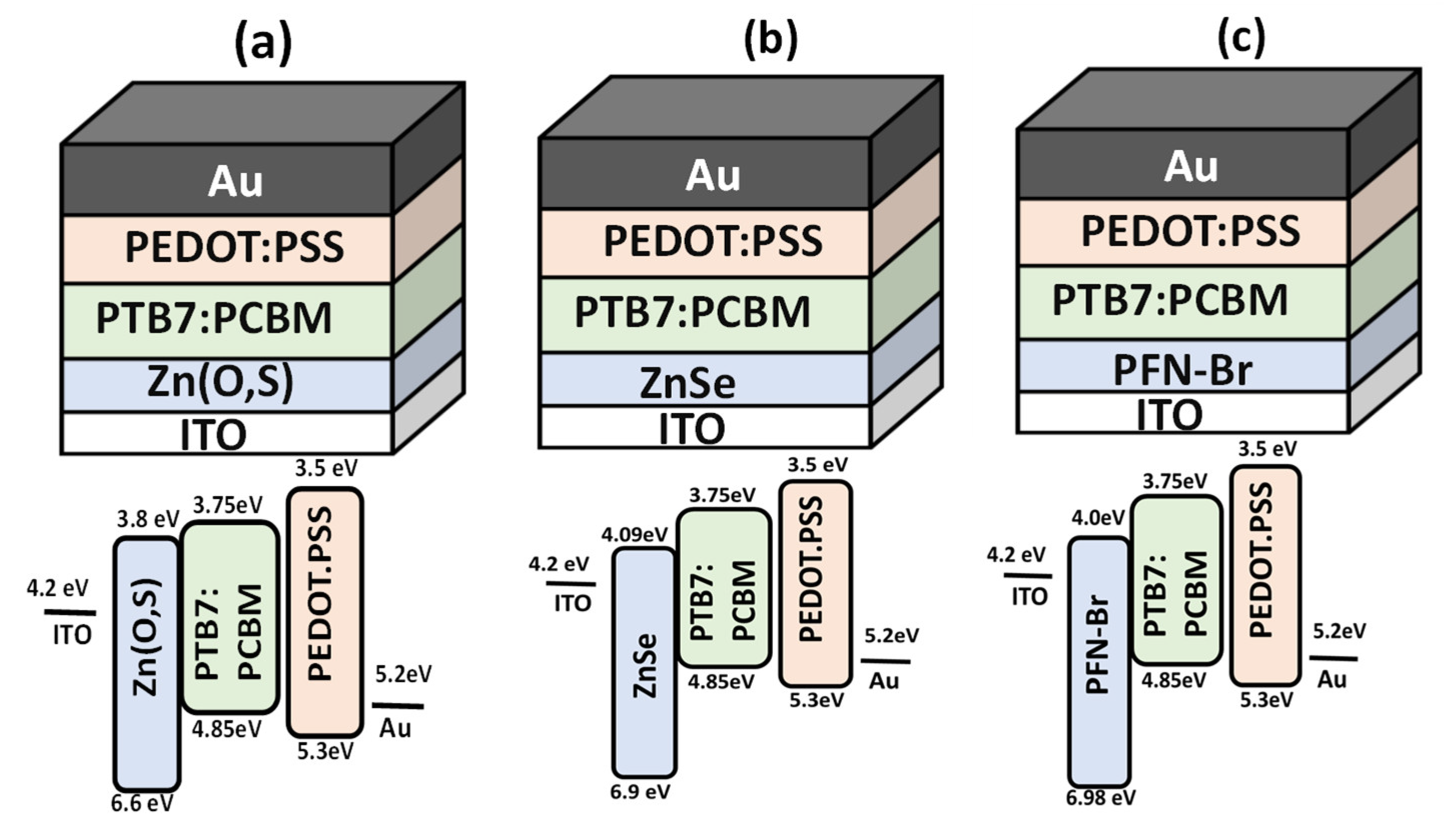
2.2. Device Structure:

The detailed photovoltaic responses of the proposed devices were investigated, evaluated, and compared as a function of the different electron transport layers. These devices are
  • ITO/Zn(O,S)/PTB7:PC70BM/PEDOT:PSS/Ag (Zn(O,S) device);
  • ITO/ZnSe/PTB7:PC70BM/PEDOT:PSS/Ag (ZnSe device);
  • ITO/PFN-Br/PTB7:PC70BM/PEDOT:PSS/Ag (PFN-Br device).
Figure 1 shows the block diagram of each proposed device with its energy bandgap diagram. It can be observed that the conduction band (or LUMO level) of all electron transport layers is in between the conduction band of ITO and PTB7:PCBM, which is the first criterion for the selection of the electron transport layer for any solar cell.
The successive thin-film deposition of a water-soluble conducting polymer even by the spin-coating method is not an issue in modern device fabrication technology. The most popular approach for the fabrication of organic photovoltaic devices involves the use of orthogonal solvents, i.e., the alternating use of organic solvents and water for the application of consecutive layers to prevent the dissolution of the previous layers. Detailed information can be found in the literature [43].

2.3. Simulation Parameters

The quality of a simulation depends on the reliability of physical and material parameters. Therefore, all physical and materials parameters required by SCAPS-1D were carefully extracted and cited from the various literature for PTB7:PC70BM as the active BHJ layer; PEDOT:PSS as the hole transport layer; and Zn(O,S), ZnSe, and PFN-Br as the electron transport layer, and are listed in Table 1. Similar to many other semiconducting polymers/oxide materials, PTB7, PEDOT:PSS, Zn(O,S), ZnSe, and PFN-Br are considered disordered semiconducting materials. They intrinsically offer both energetic and spatial disorders that can be modeled in terms of traps [44]. The presence of these traps is one of the main causes for observing the poor photovoltaic efficiency of such solar cells. Thus, to improve the quality of the simulation, bulk trap density (1014 cm−3) is introduced in all electron transport layers as shown in Table 1. Similarly, all photovoltaic simulations were carried out via 100 mW/cm2 illumination by a standard solar simulator (A.M. 1.5) under ambient room temperature conditions.

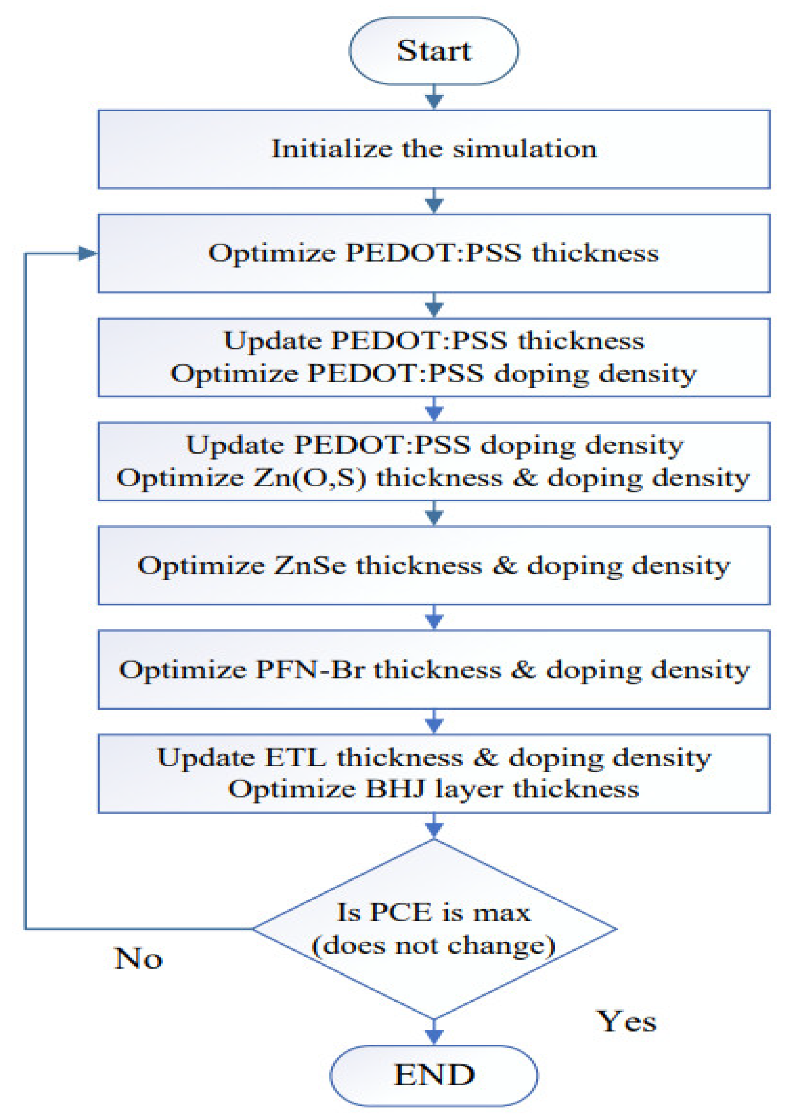
2.4. Simulation Flowchart

The general flow chart of the simulation process used in this study to determine the most suitable ETL for the proposed solar cell is shown in Figure 2. The simulation was initialized in the first stage with the suitable boundary conditions and material parameters listed in Table 1. In the second stage, the thickness of PEDOT:PSS as a hole transport layer was optimized and then updated in the SCAPS-1D software before executing the third stage. Similarly, in the third stage, the doping density of PEDOT:PSS was optimized and then updated in the SCAPS software before executing the next stage and so on. In the same way, the ETLs’ (Zn(S,O), ZnSe, and PFN-Br) thickness and doping density were optimized. In the final stage of the simulation, very small, increments/decrements (±5%) of the optimized values were varied to determine which of the proposed devices with the optimized parameters gave the maximum power conversion efficiency for the overall photovoltaic response.

3. Results and Discussion

3.1. Optimization of PEDOT:PSS Layer Thickness

According to the flow chart above, the thickness of PEDOT:PSS was optimized in the first stage, as PEDOT:PSS is the most commonly reported hole transport material for organic/inorganic type solar cells. From the published results, we did not find a PEDOT:PSS thickness above ~300 nm for any efficient photovoltaic device. Therefore, the proposed solar cells were simulated from 75 to 300 nm for the thickness optimization of the hole transport layer. Figure 3 shows the photovoltaic parameters such as open-circuit voltage, short-circuit current, fill factor, and power conversion efficiency as a function of PEDOT:PSS thickness for the Zn(S,O), ZnSe, and PFN-Br devices from 75 to 300 nm. All photovoltaic parameters slightly improved (or were nearly constant) as the thickness of PEDOT:PSS increased. If the maximum power conversion efficiency is the main criteria for determining the optimum thickness of PEDOT:PSS, then it can be inferred from the figure that 300 nm is the optimum thickness of PEDOT:PSS for all the devices, and among these, the device containing an ETL with Zn(O,S) shows the highest power conversion efficiency.
Now, the question arises of how the electron transport layer can affect the thickness of the hole transport layer. The simple answer is that the overall power conversion efficiency depends on the balance of both the electron and hole carriers collected at their respective electrodes [45,46], which in turn directly depends on the nature of the transport layer. Therefore, each device behaves differently as a function of the PEDOT:PSS layer thickness.

3.2. Optimization PEDOT:PSS Doping Density

The doping density of PEDOT:PSS was optimized in the next stage. Figure 4 shows the photovoltaic parameters such as the open-circuit voltage, short-circuit current, fill factor, and power conversion efficiency as a function of the PEDOT:PSS doping density from 1012 to 1021 cm−3 for the Zn(S, O), ZnSe, and PFN-Br devices. Similar to how the thickness of PEDOT:PSS depends on the nature of the electron transport layer as discussed above, the doping density of PEDOT:PSS also depends on the nature and parameters of the electron transport layer. Generally, the proper doping process increases the conductivity and hence improves the overall charge transport process of PEDOT:PSS as a hole transport layer. In Figure 4, the complex photovoltaic responses of the proposed devices can be seen as a function of the doping density, and the nearly constant open-circuit voltage response especially at a higher doping density confirms the formation of the ohmic contact between the anode and BHJ active layer regardless of the doping of the PEDOT:PSS for all the devices [47]. Similarly, the short-circuit current abruptly increased at ~1016 cm−3 and then became relatively constant, especially for the Zn(O,S) and ZnSe devices. As the maximum power conversion efficiency is the main criteria to determine the optimum doping of PEDOT:PSS, then it can be inferred that efficiency increased up to 1018 cm−3 for all devices and then became nearly constant so it can be justified that the 1018 cm−3 is the optimum doping of PEDOT:PSS for each device. Although the Zn(S,O) and ZnSe devices offered relatively good efficiency, the PFN-Br device showed poor photovoltaic performance.

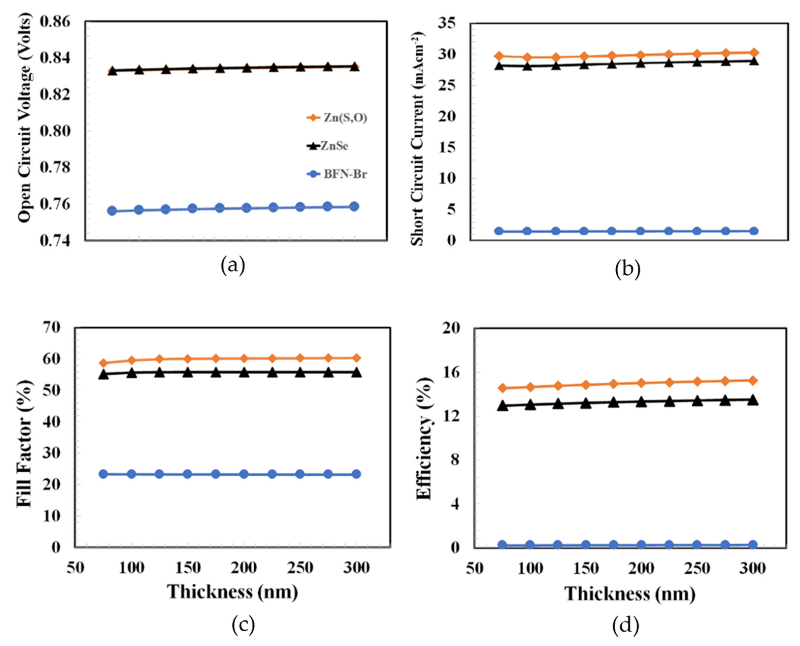
3.3. Optimization of Electron Transport Layer Thickness

The thickness optimization of the electron transport layer is more crucial compared to PEDOT:PSS because it not only helps to improve the electron transportation and collection process but also offers a path to the photons to manage the solar harvesting in the PTB7:PC70BM as the active layer. So, the electron transport layer interacts with the bulk-heterojunction layer on one side and the transparent ITO on the other side. Figure 5 shows the photovoltaic parameters such as open-circuit voltage, short-circuit current, fill factor, and power conversion efficiency as a function of the Zn(S,O), ZnSe, and PFN-Br layers’ thicknesses, which varied from 75 nm to 300 nm. Except for PFN-Br, the electron transport layers (Zn(S,O) and ZnSe) showed very similar photovoltaic responses. For the three devices, the maximum power conversion efficiencies were obtained at 75 nm. Generally, the thin electron transport layer poses some advantages such as higher built-in potential and efficient electron transport. The extra built-in potential plays a significant role in the further dissociation of excitons into the free charge carriers and offers extra drift force to further improve the transport to their respective electrodes [48,49]

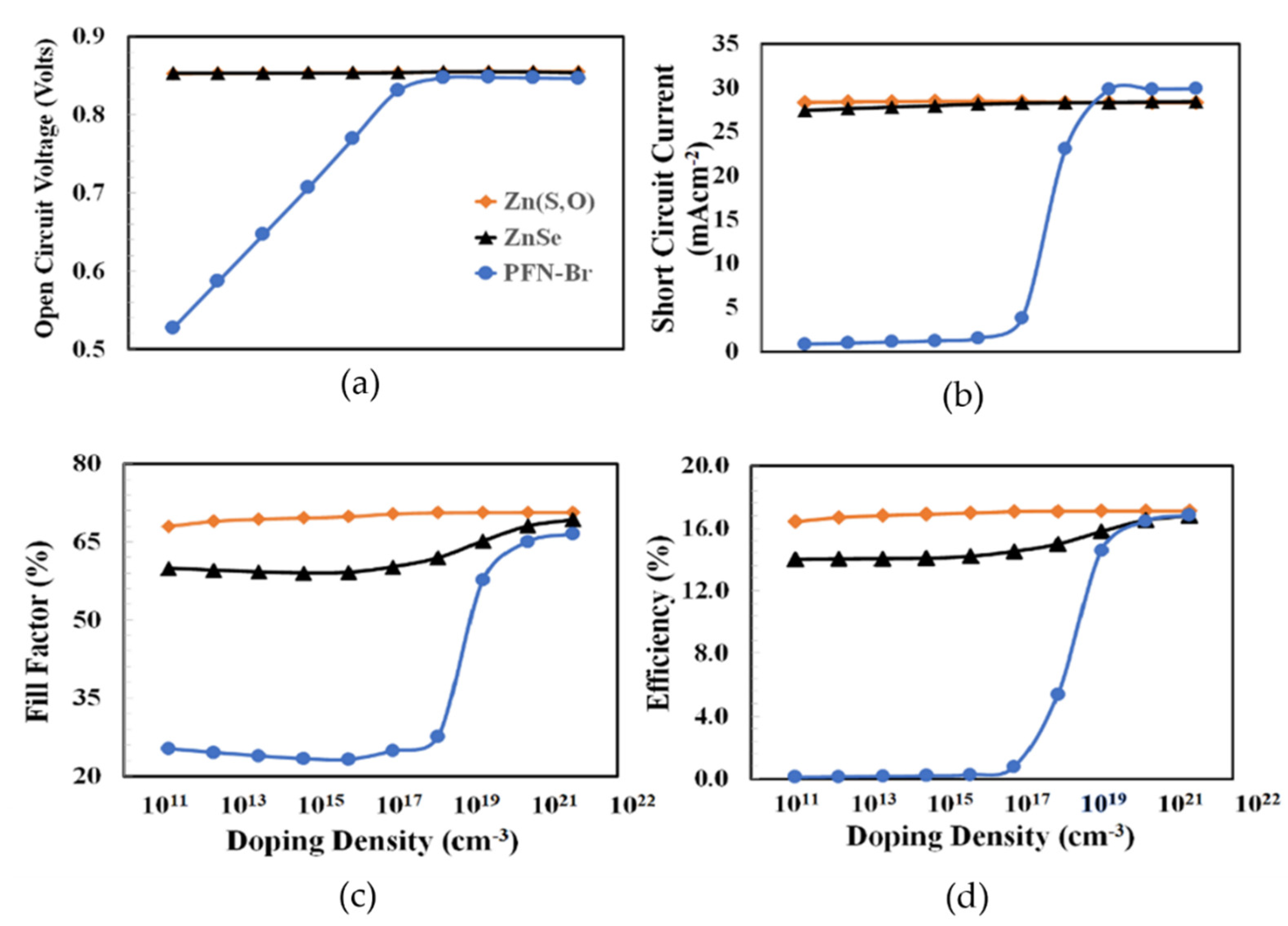
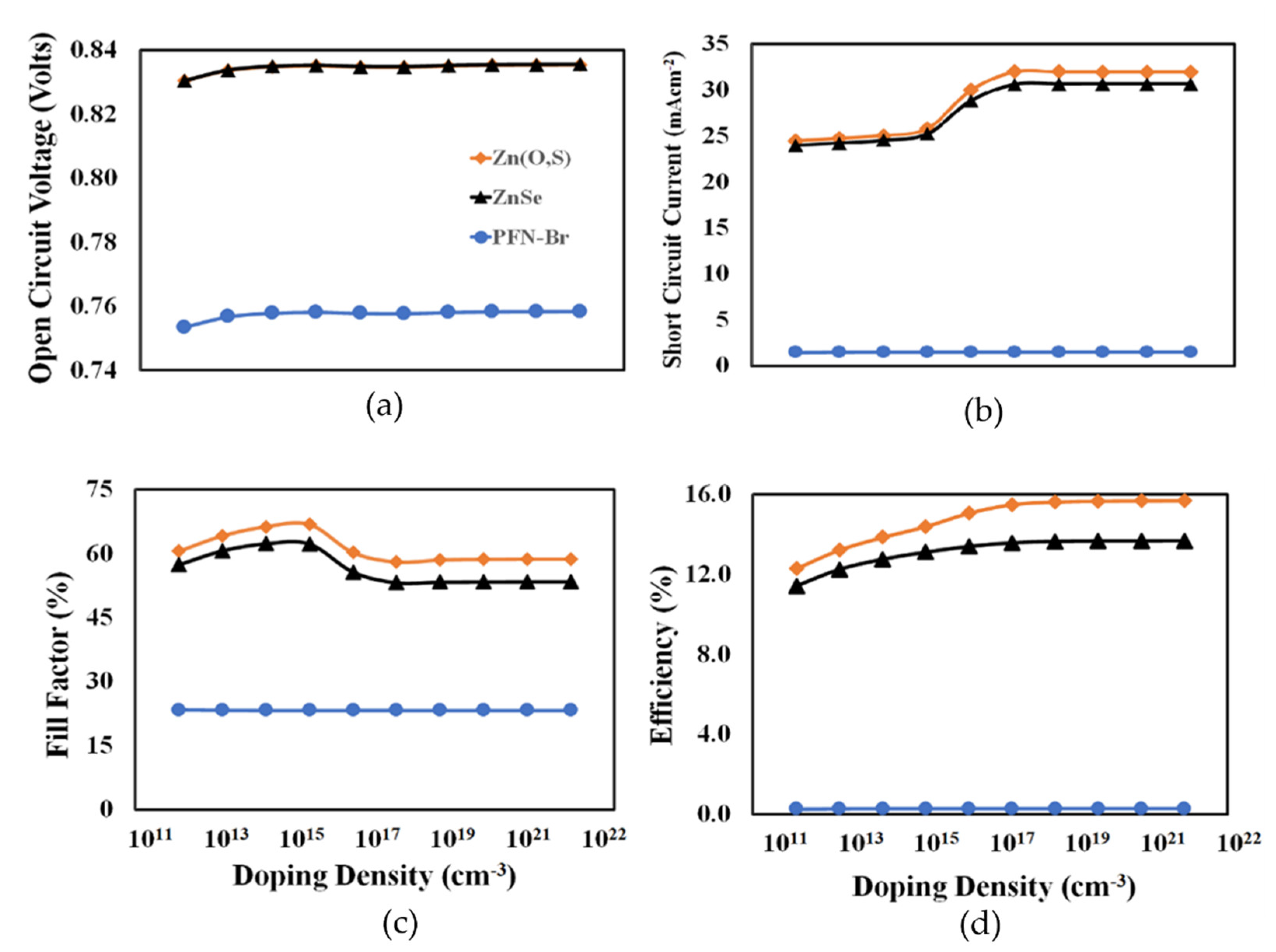
3.4. Optimization of Electron Transport Layer Doping

In the next step of the simulation, the doping density of the electron transport layer of each device was optimized. Like the hole transport layer, the optical and electrical characteristics of the electron transport layer can also be modified by appropriate doping. The proper doping of the electron transport layer causes a reduction in the bulk resistance of the transport layer, which in turn helps to improve the charge transport as well as the charge collection process and hence the overall photovoltaic performance by the formation of ohmic contact with the transparent ITO electrode [50,51,52].
Figure 6 shows the photovoltaic parameters such as open-circuit voltage, short-circuit current, fill factor, and power conversion efficiency as a function of the electron transport layer doping density for the Zn(S,O), ZnSe, and PFN-Br devices, respectively. Very complicated photovoltaic responses were observed, where all devices showed improvements in their photovoltaic parameters with the increasing doping density but at different rates. The PFN-Br device showed significant improvements, especially after doping at 1016 cm−3. Both the ZnSe and Zn(O,S) devices showed very similar increasing responses with the increasing doping density. From the results it can be inferred that the 1020 cm−3 doping density was the optimum electron transport layer doping density for all the devices, giving the maximum possible power conversion efficiency.

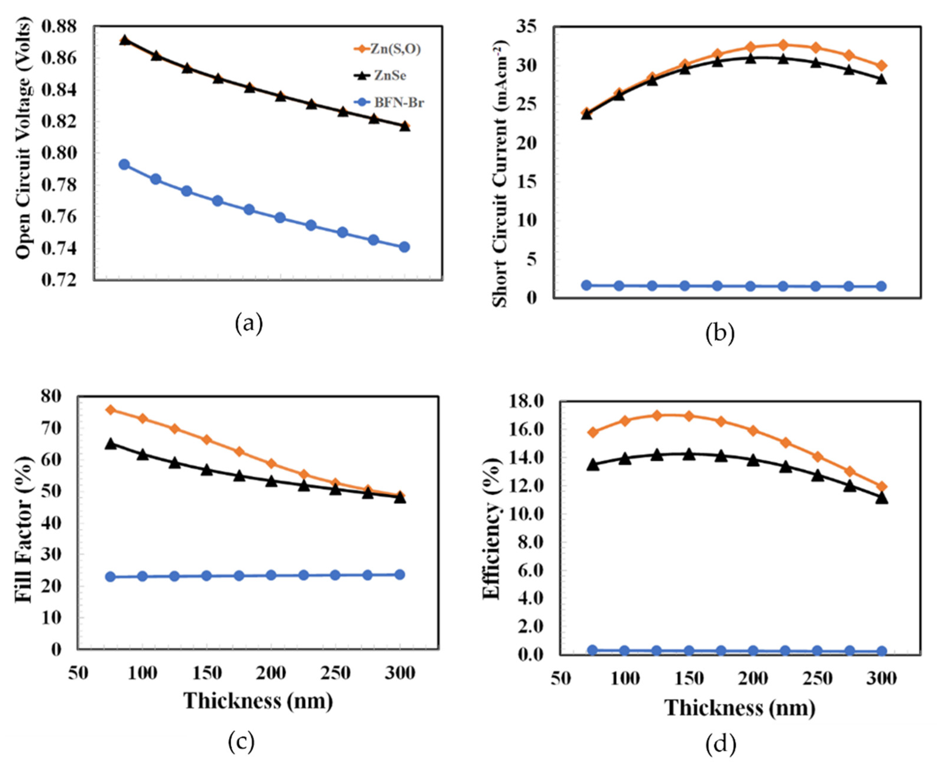
3.5. Optimization of BHJ Active Layer Thickness

As an n-i-p-type device structure was used for all the proposed photovoltaic devices, where a PTB7:PC70BM bulk-heterojunction layer was used as an insulator layer; therefore, only thickness optimization is required here for the PTB7:PC70BM bulk-heterojunction layer. The thickness optimization of an active BHJ layer is a key challenge for the improvement of photovoltaic responses. The optimum thickness of the BHJ layer is the compromise of many factors. On one side, the thickness should be so thin that it allows the dissociation of excitons into free electrons and hole pairs and as well as efficiently transports these free charges toward their respective electrodes [53,54,55]. On the other side, the thickness of the active layer should be thick enough to absorb most of the photons that fall on its surface and generate as many electron–hole pairs as possible. Generally, it is observed from the literature that most of the reported BHJ layer thicknesses for efficient polymer solar cells lie in the range of 80 to 150 nm [56,57,58].
Figure 7 shows the photovoltaic parameters such as open-circuit voltage, short-circuit current, fill factor, and power conversion efficiency as a function of the active layer thickness for the Zn(S, O), ZnSe, and PFN-B devices, respectively. The figure demonstrates that the open-circuit voltages of all the devices decreased with the increasing BHJ layer thickness because at higher thicknesses, more recombinations take place, which in turn causes a lower open-circuit voltage.
Both short-circuit current and power conversion efficiency behaved with nearly similar responses. However, initially, efficiency increased and reached a maximum value (approximately 125 nm) and then started to decrease. So, it can be inferred from the above discussion that all the parameters discussed above gave the optimum thickness of the BHJ layer at 125 nm to give the maximum power conversion efficiency for the proposed solar cell.

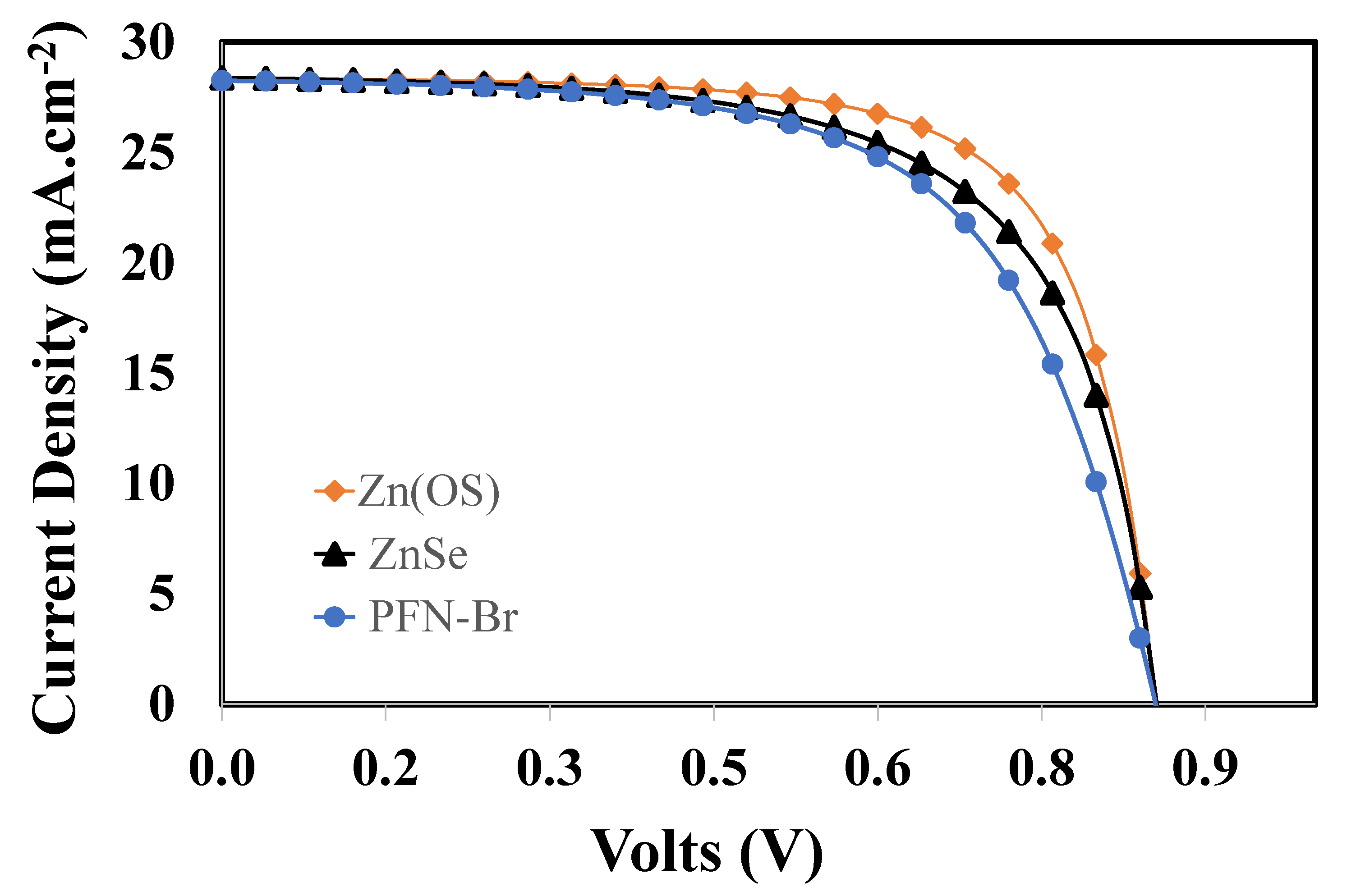
3.6. Overall Photovoltaic Response of the Proposed Devices

The overall photovoltaic current-voltage response of the proposed ITO/ETL/PTB7:PC70BM/PEDOT:PSS/Au devices were simulated and compared as shown in Figure 8, where each layer of each device was already fully optimized concerning film thickness and doping density. Here, Table 2 shows the photovoltaic parameters of each optimized device calculated from the simulated photocurrent responses (Figure 8). The simulation results clearly demonstrate that all devices performed very well, and their maximum power conversion efficiencies were found to be 17.15%, 15.81%, and 15.09% for the Zn(O,S), ZnSe, and PFN-Br devices, respectively.
The photovoltaic parameters such as the open-circuit voltages and short-circuit currents of the devices were found to offer more or less very similar maximum values within a very small range, which demonstrates that the fill factor was the decisive parameter for the selection of the highly efficient photovoltaic Zn(O,S) device compared to the other photovoltaic devices, as shown in Table 2. The fill factor (FF) is a very crucial photovoltaic parameter that demonstrates how the illuminated current-voltage response can be compared with a squared (ideal) current-voltage response for a given organic solar cell. Mathematically, the fill factor can be expressed as
F F = P i n J S C V O C = V m a x J m a x J S C V O C
where Pin, Vmax, Jmax, JSC, and VOC are the input power, maximum voltage, maximum current, short-circuit current, and open-circuit voltage, respectively. There are several independent parameters, such as mobility, series resistance, shunt resistance, morphology, and molecular weight, of both host and dopants that can significantly affect the fill factor in a very complex way [59,60]. From Table 2, it can be observed that Zn(O,S) offered the highest (70.69%) fill factor compared to ZnSe (65.15%) and PFN-Br (62.49), which could be attributed to the relatively lower built-in potential of Zn(O,S) with the PTB7:PC70BM BHJ layer [61]. Such a lower built-in potential not only improves the photovoltaic diode parameters but also improves the electron collection efficiency and hence the fill factor for the efficient photovoltaic responses. So, it can be justified that these parameters were optimized for the ITO/Zn(O,S)/PTB7:PC70BM/PEDOT:PSS/Au device to give the maximum power conversion efficiency of 17.15% compared to the other proposed devices.

4. Conclusions

In this study, a comparatively new polymer BHJ active material PTB7:PC70BM was sandwiched between efficient hole and electron transport materials. Consequently, in order to determine the most efficient solar cell, we proposed ITO/ETL/PTB7:PC70BM/PEDOT:PSS/Au with different electron transport layers, such as zinc oxysulfide (Zn(O,S)), zinc selenide (ZnSe), and poly[(9,9-bis(3′-((N,N-dimethyl)-N-ethylammonium)-propyl)-2,7-fluorene)-alt-2,7-(9,9-dioctylfluorene)] dibromide (PFN-Br), for the photovoltaic devices. Each ETL material was selected based on the energy bandgap compatibility between the ITO and PTB7:PC70BM active layer and other physical parameters. In the first stage, we optimized each layer and then simulated the photovoltaic responses through SCAPS-1D. From the photo current-voltage characteristics, it was observed that all devices behaved with nearly similar responses, whereas the ITO/Zn(O,S)/PTB7:PC70BM/PEDOT:PSS/Au device showed a maximum efficiency of up to 17.15% (Voc = 0.85 V, Jsc = 28.37 mA/cm2, and FF = 70.69%). It was also observed that these photovoltaic parameters, such as open-circuit voltage and short-circuit current, were the same for all devices, except for the fill factor. It demonstrated that the fill factor was the decisive parameter for maximum efficiency compared to the other proposed devices. The fill factor itself depends on many independent parameters such as mobility, series resistance, shunt resistance, morphology, and the molecular weight of both hosts. Therefore, it can be assumed that all these parameters were optimized for the ITO/Zn(O,S)/PTB7:PC70BM/PEDOT:PSS/Au device to give the highest power conversion efficiency of 17.15% compared to the other proposed devices.

Author Contributions

S.A.M., M.S.A. and A.N.M.A. contributed equally to the conceptualization, methodology, validation, formal analysis, and writing of the manuscript. All authors have read and agreed to the published version of the manuscript.

Funding

This research received no external funding.

Institutional Review Board Statement

Not applicable.

Informed Consent Statement

Not applicable.

Data Availability Statement

Available on the request.

Acknowledgments

The authors acknowledge the use of the SCAPS-1D program developed by Marc Burgelman et al. at the University of Gent for all the simulations reported in this work.

Conflicts of Interest

The authors declare no conflict of interest.

References

  1. Perez, M.; Perez, R. Update 2022—A Fundamental Look at Supply Side Energy Reserves for the Planet. Sol. Energy Adv. 2022, 2, 100014. [Google Scholar] [CrossRef]
  2. Shafiee, S.; Topal, E. When Will Fossil Fuel Reserves Be Diminished? Energy Policy 2009, 37, 181–189. [Google Scholar] [CrossRef]
  3. Kabir, E.; Kumar, P.; Kumar, S.; Adelodun, A.A.; Kim, K.H. Solar Energy: Potential and Future Prospects. Renew. Sustain. Energy Rev. 2018, 82, 894–900. [Google Scholar] [CrossRef]
  4. Gross, R.; Leach, M.; Bauen, A. Progress in Renewable Energy. Environ. Int. 2003, 29, 105–122. [Google Scholar] [CrossRef]
  5. Dincer, I. Renewable Energy and Sustainable Development: A Crucial Review. Renew. Sustain. Energy Rev. 2000, 4, 105–122. [Google Scholar] [CrossRef]
  6. Colasante, A.; D’Adamo, I.; Morone, P. What Drives the Solar Energy Transition? The Effect of Policies, Incentives and Behavior in a Cross-Country Comparison. Energy Res. Soc. Sci. 2022, 85, 102405. [Google Scholar] [CrossRef]
  7. Liang, C.; Gu, H.; Xia, J.; Mei, S.; Pang, P.; Zhang, N.; Guo, J.; Guo, R.; Shen, Y.; Yang, S.; et al. Recent Progress in Perovskite-Based Reversible Photon–Electricity Conversion Devices. Adv. Funct. Mater. 2022, 32, 2108926. [Google Scholar] [CrossRef]
  8. Liang, C.; Xing, G. Doping Electron Transporting Layer: An Effective Method to Enhance J SC of All-Inorganic Perovskite Solar Cells. Energy Environ. Mater. 2021, 4, 500–501. [Google Scholar] [CrossRef]
  9. Saga, T. Advances in Crystalline Silicon Solar Cell Technology for Industrial Mass Production. NPG Asia Mater. 2010, 2, 96–102. [Google Scholar] [CrossRef]
  10. Ballif, C.; Haug, F.J.; Boccard, M.; Verlinden, P.J.; Hahn, G. Status and Perspectives of Crystalline Silicon Photovoltaics in Research and Industry. Nat. Rev. Mater. 2022, 7, 597–616. [Google Scholar] [CrossRef]
  11. Li, Y.; Huang, W.; Zhao, D.; Wang, L.; Jiao, Z.; Huang, Q.; Wang, P.; Sun, M.; Yuan, G. Recent Progress in Organic Solar Cells: A Review on Materials from Acceptor to Donor. Molecules 2022, 27, 1800. [Google Scholar] [CrossRef] [PubMed]
  12. Moiz, S.A.; Alahmadi, A.N.M.; Karimov, K.S. Improved Organic Solar Cell by Incorporating Silver Nanoparticles Embedded Polyaniline as Buffer Layer. Solid-State Electron. 2020, 163, 107658. [Google Scholar] [CrossRef]
  13. Helgesen, M.; Søndergaard, R.; Krebs, F.C. Advanced Materials and Processes for Polymer Solar Cell Devices. J. Mater. Chem. 2010, 20, 36–60. [Google Scholar] [CrossRef]
  14. Kuik, M.; Wetzelaer, G.J.A.H.; Nicolai, H.T.; Craciun, N.I.; de Leeuw, D.M.; Blom, P.W.M. 25th Anniversary Article: Charge Transport and Recombination in Polymer Light-Emitting Diodes. Adv. Mater. 2014, 26, 512–531. [Google Scholar] [CrossRef]
  15. Garnier, F.; Hajlaoui, R.; Yassar, A.; Srivastava, P. All-Polymer Field-Effect Transistor Realized by Printing Techniques. Science 1994, 265, 1684–1686. [Google Scholar] [CrossRef] [PubMed]
  16. Harsányi, G. Polymer films in sensor applications: A review of present uses and future possibilities. Sens. Rev. 2000, 20, 98–105. [Google Scholar] [CrossRef]
  17. Cichosz, S.; Masek, A.; Zaborski, M. Polymer-based sensors: A review. Polym. Test. 2018, 67, 342–348. [Google Scholar] [CrossRef]
  18. Yin, H.; Yan, C.; Hu, H.; Ho, J.K.W.; Zhan, X.; Li, G.; So, S.K. Recent Progress of All-Polymer Solar Cells—From Chemical Structure and Device Physics to Photovoltaic Performance. Mater. Sci. Eng. R Rep. 2020, 140, 100542. [Google Scholar] [CrossRef]
  19. Brédas, J.L.; Norton, J.E.; Cornil, J.; Coropceanu, V. Molecular Understanding of Organic Solar Cells: The Challenges. ACC Chem. Res. 2009, 42, 1691–1699. [Google Scholar] [CrossRef]
  20. Hendry, E.; Schins, J.M.; Candeias, L.P.; Siebbeles, L.D.A.; Bonn, M. Efficiency of Exciton and Charge Carrier Photogeneration in a Semiconducting Polymer. Phys. Rev. Lett. 2004, 92, 196601. [Google Scholar] [CrossRef] [Green Version]
  21. Moiz, S.A.; Nahhas, A.M.; Um, H.-D.; Jee, S.-W.; Cho, H.K.; Kim, S.-W.; Lee, J.-H. A Stamped PEDOT:PSS–Silicon Nanowire Hybrid Solar Cell. Nanotechnology 2012, 23, 145401. [Google Scholar] [CrossRef] [PubMed]
  22. Heeger, A.J. 25th Anniversary Article: Bulk Heterojunction Solar Cells: Understanding the Mechanism of Operation. Adv. Mater. 2014, 26, 10–28. [Google Scholar] [CrossRef] [PubMed]
  23. Zhao, W.; Li, S.; Yao, H.; Zhang, S.; Zhang, Y.; Yang, B.; Hou, J. Molecular Optimization Enables over 13% Efficiency in Organic Solar Cells. J. Am. Chem. Soc. 2017, 139, 7148–7151. [Google Scholar] [CrossRef] [PubMed]
  24. Kang, H.; Kim, G.; Kim, J.; Kwon, S.; Kim, H.; Lee, K. Bulk-Heterojunction Organic Solar Cells: Five Core Technologies for Their Commercialization. Adv. Mater. 2016, 28, 7821–7861. [Google Scholar] [CrossRef]
  25. He, Z.; Zhong, C.; Su, S.; Xu, M.; Wu, H.; Cao, Y. Enhanced Power-Conversion Efficiency in Polymer Solar Cells Using an Inverted Device Structure. Nat. Photonics 2012, 6, 591–595. [Google Scholar] [CrossRef]
  26. Kwiatkowska, E.; Mech, W.; Wincukiewicz, A.; Korona, K.P.; Zarębska, K.; Kamińska, M.; Skompska, M. Investigation of Polyaniline Doped with Camphorsulfonic Acid in Chloroform Solution as a Hole Transporting Layer in PTB7: PCBM and Perovskite-Based Solar Cells. Electrochim. Acta 2021, 380, 138264. [Google Scholar] [CrossRef]
  27. Alahmadi, A.N.M. Design of an Efficient PTB7:PC70BM-Based Polymer Solar Cell for 8% Efficiency. Polymers 2022, 14, 889. [Google Scholar] [CrossRef]
  28. Ratcliff, E.L.; Zacher, B.; Armstrong, N.R. Selective Interlayers and Contacts in Organic Photovoltaic Cells. J. Phys. Chem. Lett. 2011, 2, 1337–1350. [Google Scholar] [CrossRef] [PubMed]
  29. Girtan, M.; Rusu, M. Role of ITO and PEDOT: PSS in Stability/Degradation of Polymer: Fullerene Bulk Heterojunctions Solar Cells. Sol. Energy Mater. Sol. Cells 2010, 94, 446–450. [Google Scholar] [CrossRef]
  30. Moiz, S.A.; Alahmadi, A.N.M.; Aljohani, A.J. Design of Silicon Nanowire Array for PEDOT: PSS-Silicon Nanowire-Based Hybrid Solar Cell. Energies 2020, 13, 3797. [Google Scholar] [CrossRef]
  31. Moiz, S.A.; Alahmadi, A.N.M.; Aljohani, A.J. Design of a Novel Lead-Free Perovskite Solar Cell for 17.83% Efficiency. IEEE Access 2021, 9, 54254–54263. [Google Scholar] [CrossRef]
  32. van Dijken, A.; Perro, A.; Meulenkamp, E.A.; Brunner, K. The Influence of a PEDOT:PSS Layer on the Efficiency of a Polymer Light-Emitting Diode. Org. Electron. 2003, 4, 131–141. [Google Scholar] [CrossRef]
  33. Nguyen, T.P.; le Rendu, P.; Long, P.D.; de Vos, S.A. Chemical and Thermal Treatment of PEDOT:PSS Thin Films for Use in Organic Light Emitting Diodes. Surf. Coat. Technol. 2004, 180–181, 646–649. [Google Scholar] [CrossRef]
  34. Zhao, X.; Zhan, X. Electron Transporting Semiconducting Polymers in Organic Electronics. Chem. Soc. Rev. 2011, 40, 3728–3743. [Google Scholar] [CrossRef] [PubMed]
  35. Lee, S.; Paine, D.C.; Gleason, K.K. Heavily Doped poly (3,4-ethylenedioxythiophene) Thin Films with High Carrier Mobility Deposited Using Oxidative CVD: Conductivity Stability and Carrier Transport. Adv. Funct. Mater. 2014, 24, 7187–7196. [Google Scholar] [CrossRef]
  36. Shao, G. Work function and electron affinity of semiconductors: Doping effect and complication due to fermi level pinning. Energy Environ. Mater. 2021, 4, 273–276. [Google Scholar] [CrossRef]
  37. Burgelman, M.; Nollet, P.; Degrave, S. Modelling Polycrystalline Semiconductor Solar Cells. Thin Solid Film. 2000, 361, 527–532. [Google Scholar] [CrossRef]
  38. Minbashi, M.; Omrani, M.K.; Memarian, N.; Kim, D.H. Comparison of Theoretical and Experimental Results for Band-Gap-Graded CZTSSe Solar Cell. Curr. Appl. Phys. 2017, 17, 1238–1243. [Google Scholar] [CrossRef]
  39. Verschraegen, J.; Burgelman, M. Numerical Modeling of Intra-Band Tunneling for Heterojunction Solar Cells in Scaps. Thin Solid Film. 2007, 515, 6276–6279. [Google Scholar] [CrossRef]
  40. Dridi, C.; Touafek, N.; Mahamdi, R. Inverted PTB7: PC70BM Bulk Heterojunction Solar Cell Device Simulations for Various Inorganic Hole Transport Materials. Optik 2022, 252, 168447. [Google Scholar] [CrossRef]
  41. Chiew, E.K.; Yahaya, M.; Othman, A.P. Electrical Characterization of P3HT/PCBM Bulk Heterojunction Organic Solar Cell. Int. J. Comput. Mater. Sci. Eng. 2012, 01, 1250004. [Google Scholar] [CrossRef]
  42. Moiz, S.A.; Alahmadi, A.N.M. Design of Dopant and Lead-Free Novel Perovskite Solar Cell for 16.85% Efficiency. Polymers 2021, 13, 2110. [Google Scholar] [CrossRef] [PubMed]
  43. Aguirre, J.C.; Hawks, S.A.; Ferreira, A.S.; Yee, P.; Subramaniyan, S.; Jenekhe, S.A.; Tolbert, S.H.; Schwartz, B.J. Sequential Processing for Organic Photovoltaics: Design Rules for Morphology Control by Tailored Semi-Orthogonal Solvent Blends. Adv. Energy Mater. 2015, 5, 1402020. [Google Scholar] [CrossRef]
  44. Groves, C.; Blakesley, J.C.; Greenham, N.C. Effect of charge trapping on geminate recombination and polymer solar cell performance. Nano Lett. 2010, 10, 1063–1069. [Google Scholar] [CrossRef] [PubMed]
  45. Hu, Z.; Zhang, J.; Hao, Z.; Zhao, Y. Influence of Doped PEDOT: PSS on the Performance of Polymer Solar Cells. Sol. Energy Mater. Sol. Cells 2011, 95, 2763–2767. [Google Scholar] [CrossRef]
  46. Chi, D.; Huang, S.; Yue, S.; Liu, K.; Lu, S.; Wang, Z.; Qu, S.; Wang, Z. Ultra-Thin ZnO Film as an Electron Transport Layer for Realizing the High Efficiency of Organic Solar Cells. RSC Adv. 2017, 7, 14694–14700. [Google Scholar] [CrossRef]
  47. Swami, S.K.; Chaturvedi, N.; Kumar, A.; Kumar, V.; Garg, A.; Dutta, V. Spray Deposited Gallium Doped Zinc Oxide (GZO) Thin Film as the Electron Transport Layer in Inverted Organic Solar Cells. Sol. Energy 2022, 231, 458–463. [Google Scholar] [CrossRef]
  48. Lee, S.; Lee, J.H.; Lee, J.H.; Kim, J.J. The Mechanism of Charge Generation in Charge-Generation Units Composed of p-Doped Hole-Transporting Layer/HATCN/n-Doped Electron-Transporting Layers. Adv. Funct. Mater. 2012, 22, 855–860. [Google Scholar] [CrossRef]
  49. Yap, C.C.; Yahaya, M.; Salleh, M.M. Influence of Thickness of Functional Layer on Performance of Organic Salt-Doped OLED with ITO/PVK:PBD:TBAPF6/Al Structure. Curr. Appl. Phys. 2008, 8, 637–644. [Google Scholar] [CrossRef]
  50. Ratcliff, E.L.; Lee, P.A.; Armstrong, N.R. Work Function Control of Hole-Selective Polymer/ITO Anode Contacts: An Electrochemical Doping Study. J. Mater. Chem. 2010, 20, 2672–2679. [Google Scholar] [CrossRef]
  51. Kirchartz, T.; Agostinelli, T.; Campoy-Quiles, M.; Gong, W.; Nelson, J. Understanding the Thickness-Dependent Performance of Organic Bulk Heterojunction Solar Cells: The Influence of Mobility, Lifetime, and Space Charge. J. Phys. Chem. Lett. 2012, 3, 3470–3475. [Google Scholar] [CrossRef] [PubMed]
  52. Moiz, S.A. Optimization of Hole and Electron Transport Layer for Highly Efficient Lead-Free Cs2TiBr6-Based Perovskite Solar Cell. Photonics 2022, 9, 23. [Google Scholar] [CrossRef]
  53. Blom, P.W.M.; Mihailetchi, V.D.; Koster, L.J.A.; Markov, D.E. Device Physics of Polymer: Fullerene Bulk Heterojunction Solar Cells. Adv. Mater. 2007, 19, 1551–1566. [Google Scholar] [CrossRef]
  54. Waldauf, C.; Scharber, M.C.; Schilinsky, P.; Hauch, J.A.; Brabec, C.J. Physics of Organic Bulk Heterojunction Devices for Photovoltaic Applications. J. Appl. Phys. 2006, 99, 104503. [Google Scholar] [CrossRef]
  55. Gasparini, N.; Wadsworth, A.; Moser, M.; Baran, D.; McCulloch, I.; Brabec, C.J. The Physics of Small Molecule Acceptors for Efficient and Stable Bulk Heterojunction Solar Cells. Adv. Energy Mater. 2018, 8, 1703298. [Google Scholar] [CrossRef]
  56. Nam, S.; Seo, J.; Woo, S.; Kim, W.H.; Kim, H.; Bradley, D.D.C.; Kim, Y. Inverted Polymer Fullerene Solar Cells Exceeding 10% Efficiency with Poly(2-Ethyl-2-Oxazoline) Nanodots on Electron-Collecting Buffer Layers. Nat. Commun. 2015, 6, 8929. [Google Scholar] [CrossRef]
  57. Yao, H.; Zhao, W.; Zheng, Z.; Cui, Y.; Zhang, J.; Wei, Z.; Hou, J. PBDT-TSR: A Highly Efficient Conjugated Polymer for Polymer Solar Cells with a Regioregular Structure. J. Mater. Chem. A 2016, 4, 1708–1713. [Google Scholar] [CrossRef]
  58. Ye, L.; Zhang, S.; Zhao, W.; Yao, H.; Hou, J. Highly Efficient 2D-Conjugated Benzodithiophene-Based Photovoltaic Polymer with Linear Alkylthio Side Chain. Chem. Mater. 2014, 26, 3603–3605. [Google Scholar] [CrossRef]
  59. Jao, M.H.; Liao, H.C.; Su, W.F. Achieving a High Fill Factor for Organic Solar Cells. J. Mater. Chem. A 2016, 4, 5784–5801. [Google Scholar] [CrossRef]
  60. Qi, B.; Wang, J. Fill Factor in Organic Solar Cells. Phys. Chem. Chem. Phys. 2013, 15, 8972–8982. [Google Scholar] [CrossRef]
  61. Korir, B.K.; Kibet, J.K.; Ngari, S.M. Computational Simulation of a Highly Efficient Hole Transport-Free Dye-Sensitized Solar Cell Based on Titanium Oxide (TiO2) and Zinc Oxysulfide (ZnOS) Electron Transport Layers. J. Electron. Mater. 2021, 50, 7259–7274. [Google Scholar] [CrossRef]
Figure 1. The device block structure and energy band diagram for (a) ITO/Zn(O,S)/PTB7:PC70BM/PEDOT:PSS/Au, (b) ITO/ZnSe/PTB7:PC70BM/PEDOT:PSS/Au, (c) ITO/PFN-Br/PTB7:PC70BM/PEDOT:PSS/Au.
Polymers 14 03610 g001
Figure 2. Shows the flow chart used to determine the maximum power-conversion efficiency of the proposed photovoltaic ITO/ETL/PTB7:PC70BM/PEDOT:PSS/Au devices with various ETL (Zn(O,S), ZnSe, and PFN-Br) layers.
Polymers 14 03610 g002
Figure 3. Shows the photovoltaic parameters of (a) open-circuit voltage, (b) short-circuit current, (c) fill factor, and (d) power conversion efficiency as a function of PEDOT:PSS thickness for ITO/Zn(O,S)/PTB7:PC70BM/PEDOT:PSS/Au, ITO/ZnSe/PTB7:PC70BM/PEDOT:PSS/Au, ITO/PFN-Br/PTB7:PC70BM/PEDOT:PSS/Au, respectively.
Polymers 14 03610 g003
Figure 4. The photovoltaic parameters of (a) open-circuit voltage, (b) short-circuit current, (c) fill factor, and (d) power conversion efficiency as a function of the PEDOT:PSS doping density for ITO/Zn(O,S)/PTB7:PC70BM/PEDOT:PSS/Au, ITO/ZnSe/PTB7:PC70BM/PEDOT:PSS/Au, ITO/PFN-Br/PTB7:PC70BM/PEDOT:PSS/Au, respectively.
Polymers 14 03610 g004
Figure 5. The photovoltaic parameters of (a) open-circuit voltage, (b) short-circuit current, (c) fill factor, and (d) power conversion efficiency as a function of electron transport layer (Zn(O,S), ZnSe, PFN-Br) thickness for TO/Zn(O,S)/PTB7:PC70BM/PEDOT:PSS/Au, ITO/ZnSe/PTB7:PC70BM/PEDOT:PSS/Au, ITO/PFN-Br/PTB7:PC70BM/PEDOT:PSS/Au, respectively.
Polymers 14 03610 g005
Figure 6. The photovoltaic parameters of (a) open-circuit voltage, (b) short-circuit current, (c) fill factor, and (d) power conversion efficiency as a function of the electron transport layer (Zn(O,S), ZnSe, PFN-Br) doping density for ITO/Zn(O,S)/PTB7:PC70BM/PEDOT:PSS/Au, ITO/ZnSe/PTB7:PC70BM/PEDOT:PSS/Au, ITO/PFN-Br/PTB7:PC70BM/PEDOT:PSS/Au, respectively.
Polymers 14 03610 g006
Figure 7. The photovoltaic parameters of (a) open-circuit voltage, (b) short-circuit current, (c) fill factor, and (d) power conversion efficiency as a function of the PTB7:PCBM active layer thickness for ITO/Zn(O,S)/PTB7:PCBM/PEDOT:PSS/Au, ITO/ZnSe/PTB7:PCBM/PEDOT:PSS/Au, ITO/PFN-Br/PTB7:PCBM/PEDOT:PSS/Au, respectively.
Polymers 14 03610 g007
Figure 8. The overall photovoltage parameters of the optimized devices ITO/Zn(O,S)/PTB7:PC70BM/PEDOT:PSS/Au, ITO/ZnSe/PTB7:PC70BM/PEDOT:PSS/Au, ITO/PFN-Br/PTB7:PC70BM/PEDOT:PSS/Au, respectively.
Polymers 14 03610 g008
Table 1. The physical and material parameters of the active BHJ, hole transport, and electron transport layers used in the simulation, as required by SCAPS-1D.
ParametersSymbolUnitPEDOT:PSSBHJETL
Zn(O,S)ZnSePFN-Br
ThicknessTnm300300757575
Energy Band GapEgeV1.801.102.82.812.98
Electron AffinityΧeV3.503.753.804.094.00
Dielectric Permittivity εr-3.003.909.008.605.00
Effective Density of States at Conduction Band NCcm−32.2 × 10186 × 10192.2 × 1018 2.2 × 10¹⁸ 1.0 × 10¹⁹
Effective Density of States at Valance Band NVcm−31.8 × 10¹⁹ 2.0 × 10¹⁹ 1.8 × 10¹⁹ 1.8 × 10¹⁸ 1.0 × 10¹⁹
Electron Thermal Velocity Vecm/s1.0 × 107 1.0 × 10⁷ 1.0 × 10⁷ 1.0 × 10⁷ 1.0 × 10⁷
Hole Thermal Velocity Vhcm/s1.0 × 107 1.0 × 10⁷ 1.0 × 10⁷ 1.0 × 10⁷ 1.0 × 10⁷
Electron Mobility µecm2/V·s14.4 × 10−4 1.0 × 10² 4.0 × 10² 2.0 × 10⁻⁶
Hole Mobilityµhcm2/V·s2.0 × 101 2.5 × 10⁻⁴ 2.5 × 101 1.1 × 10² 1.0 × 10⁻⁴
Donor Density NDcm−3-1.0 × 10¹⁹ 1.0 × 10¹⁹ 1.0 × 10¹⁹ 1.0 × 10¹⁹
Hole Density NAcm−31.0 × 10¹⁸ 1.0 × 10¹⁹ ---
Defect Density Ntcm−31.0 × 10¹⁴ 1.0 × 10¹⁴ 1.0 × 10¹⁴ 1.0 × 10¹⁴ 1.0 × 10¹⁴
Table 2. The overall photovoltaic parameters for the optimized Zn(O,S), ZnSe, and PFN-Br devices.
ETLVoc (Volt)Jsc
(mA/cm2)
FF (%)PCE (%)
Zn(O,S)0.854928.37670.6917.15
ZnSe0.855128.37065.1515.81
PFN-Br0.854628.25562.4915.09
Publisher’s Note: MDPI stays neutral with regard to jurisdictional claims in published maps and institutional affiliations.

