
Development of a Custom-Made 3D Printing Protocol with Commercial Resins for Manufacturing Microfluidic Devices

 ,
,  ,
, 
Abstract
:1. Introduction
2. Materials and Methods
2.1. 3D Printer
2.2. Resins Used and Absorbance Test
2.3. 3D Printing Protocol
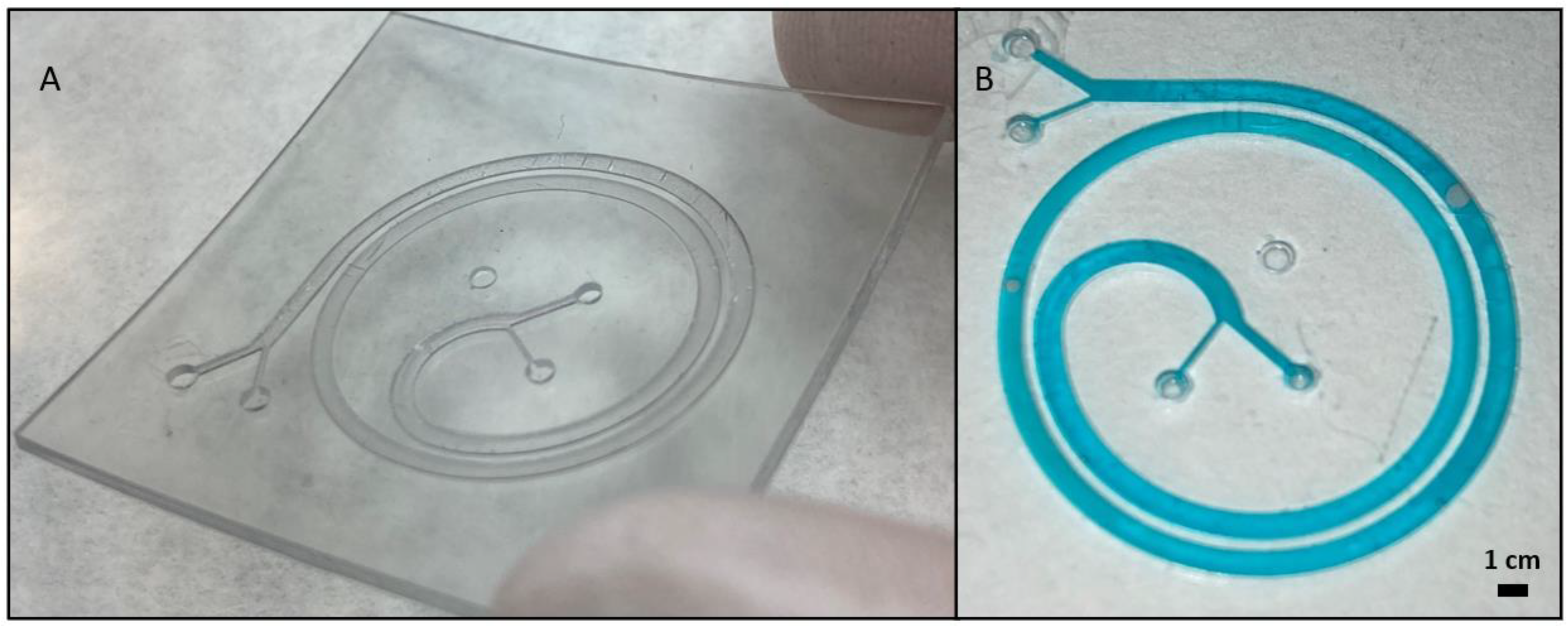
2.4. Chip Manufacturing
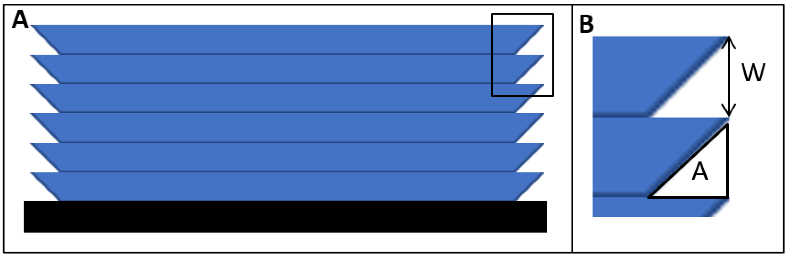
2.5. Dimensional Characterization
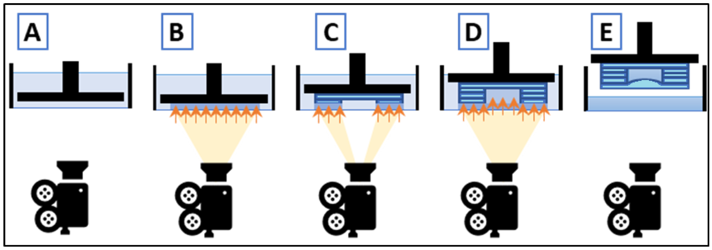
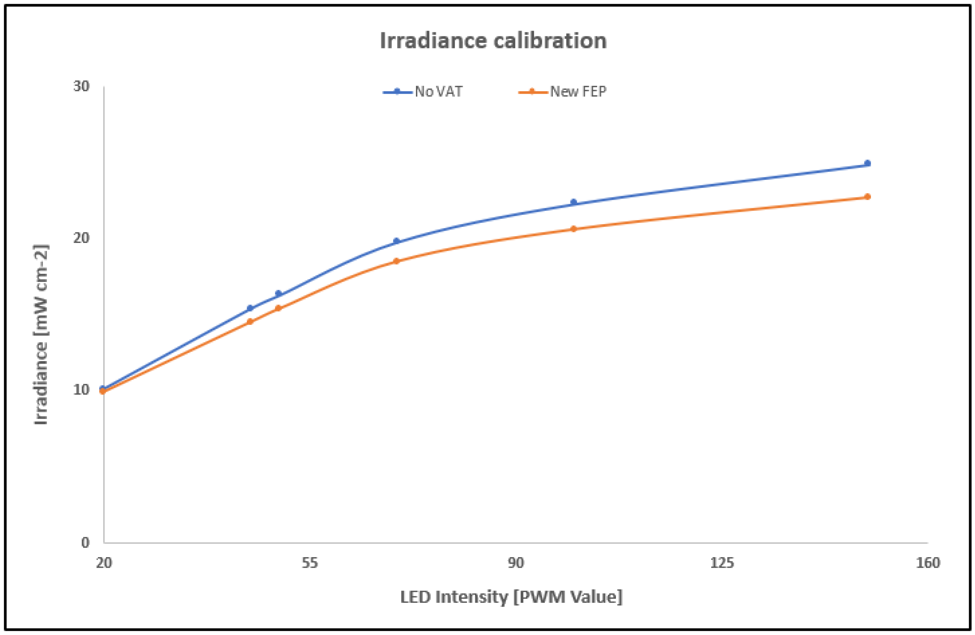
2.6. Projector Irradiance Calibration
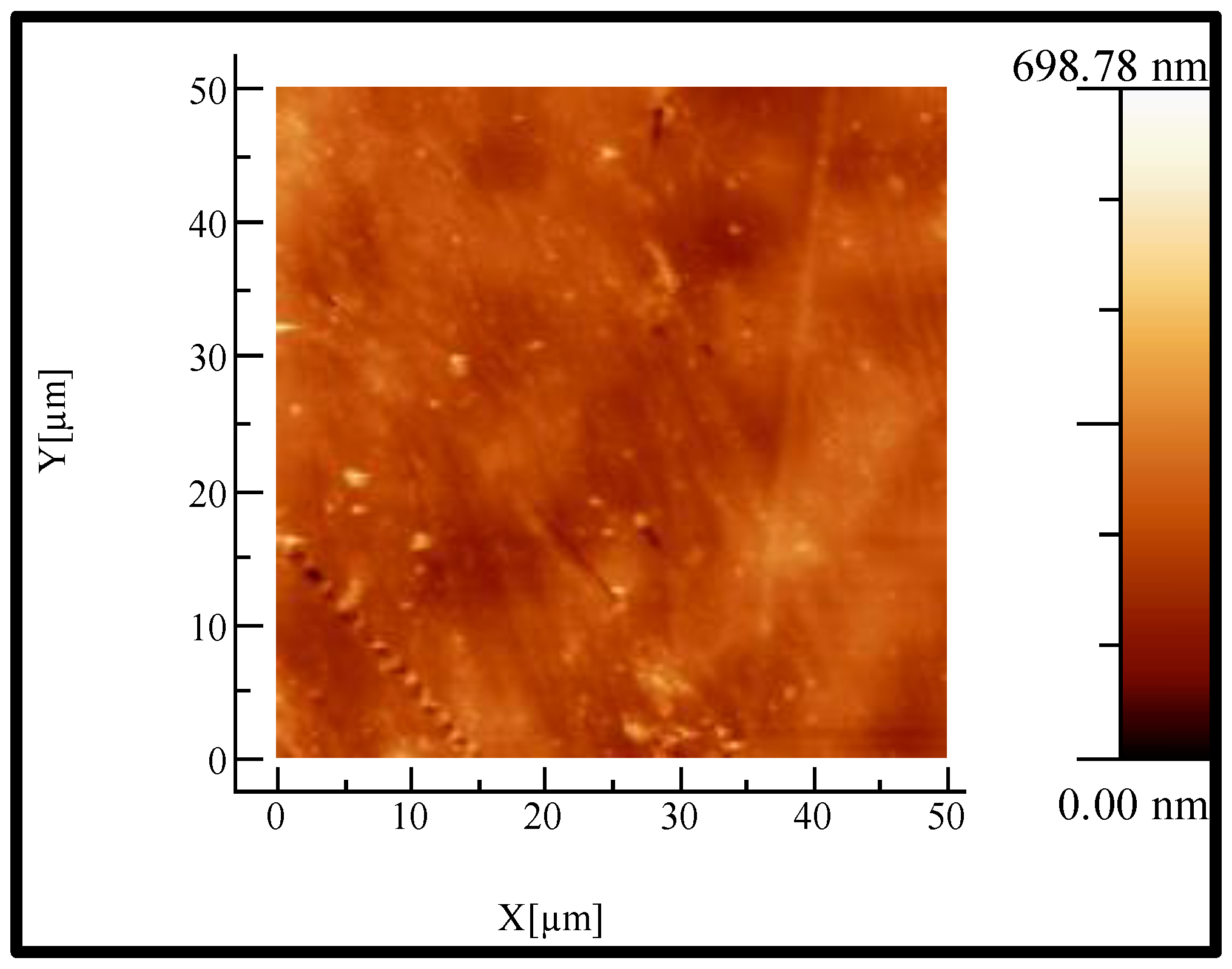
2.7. Rugosity Test Atomic Force Microscopy
3. Results
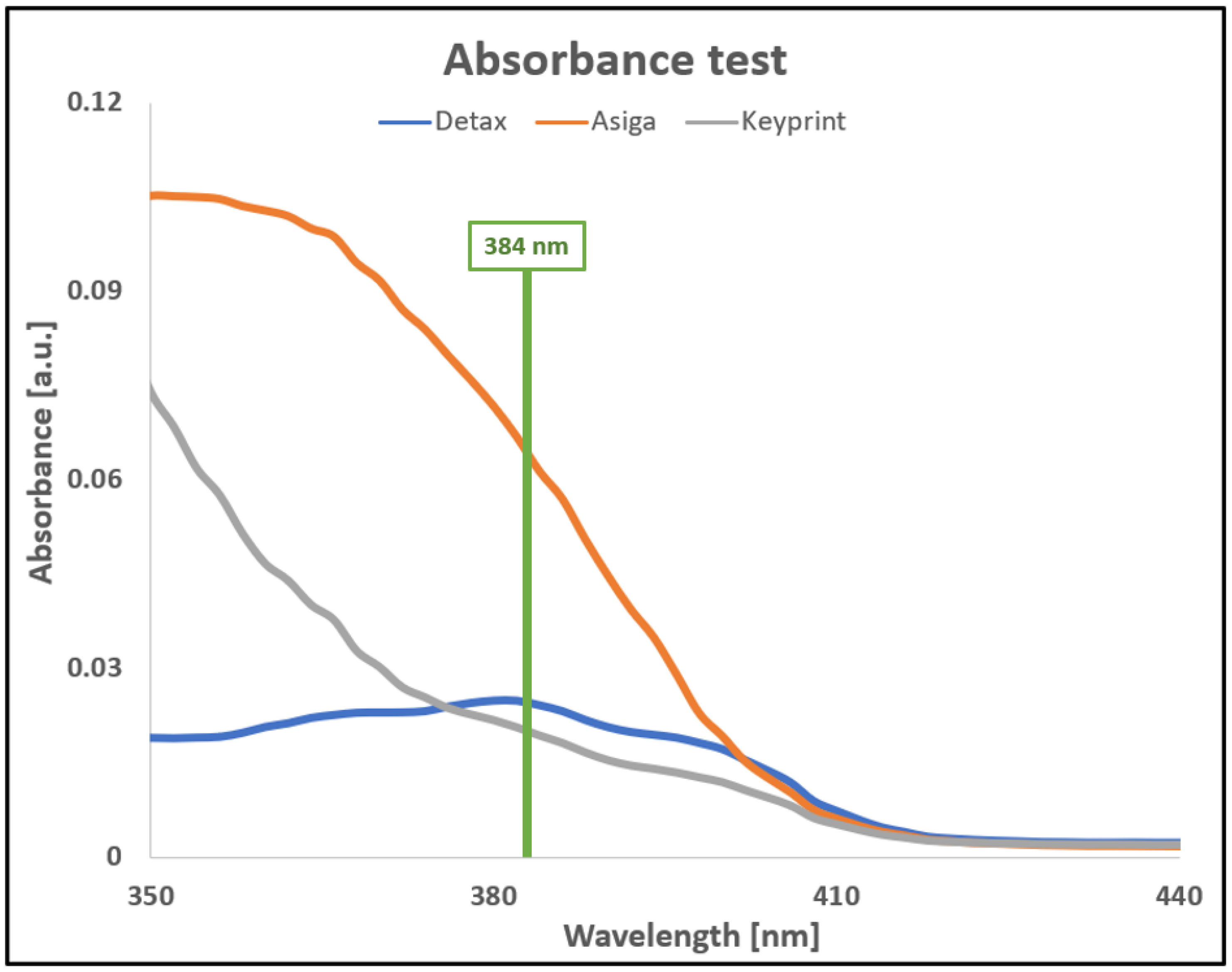
3.1. Absorbance Characterization
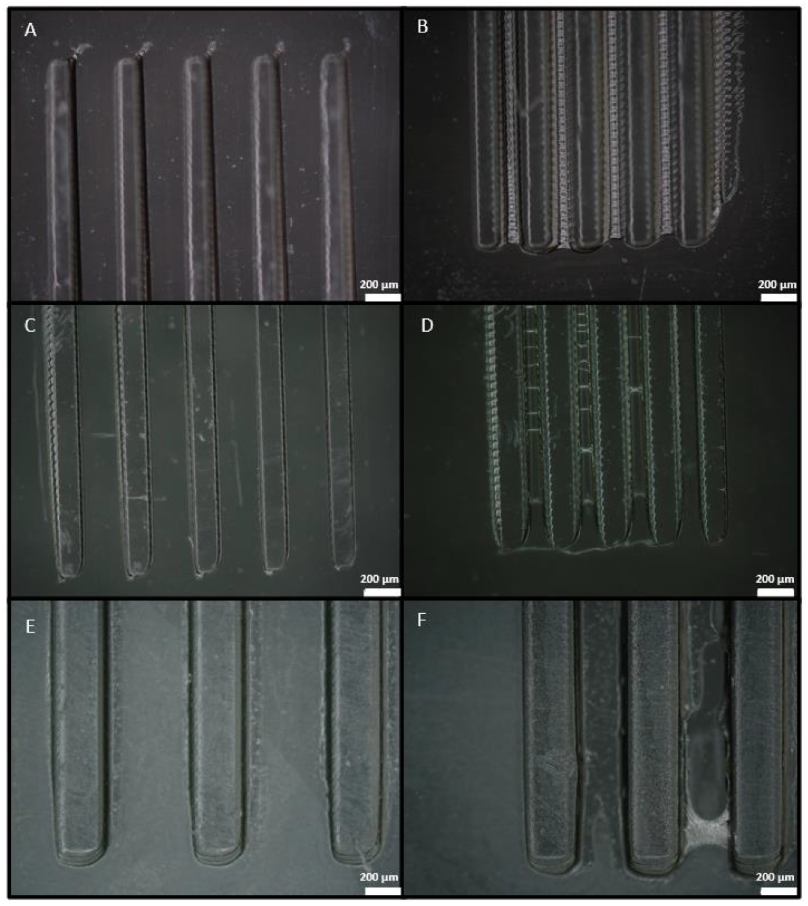
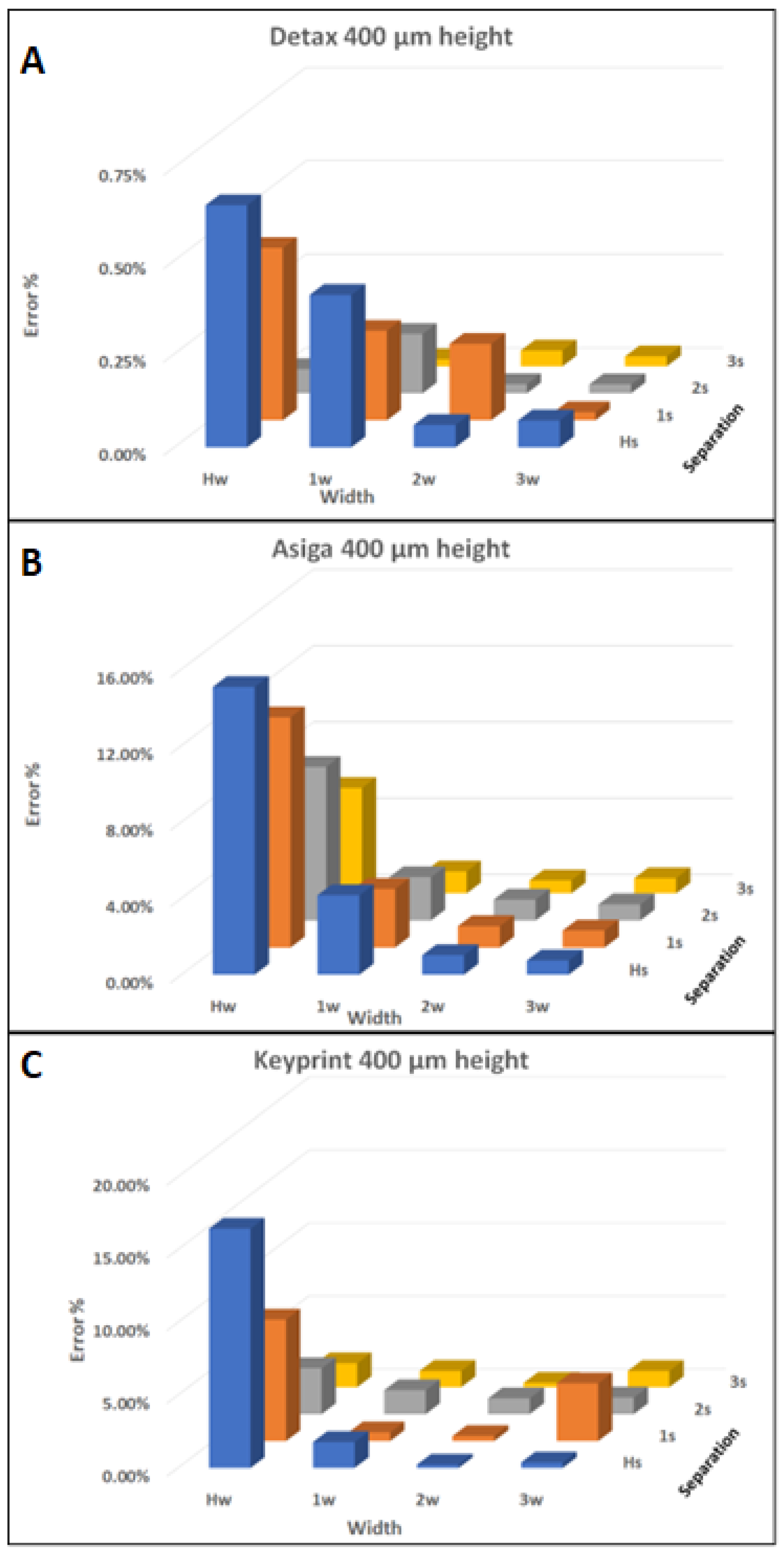
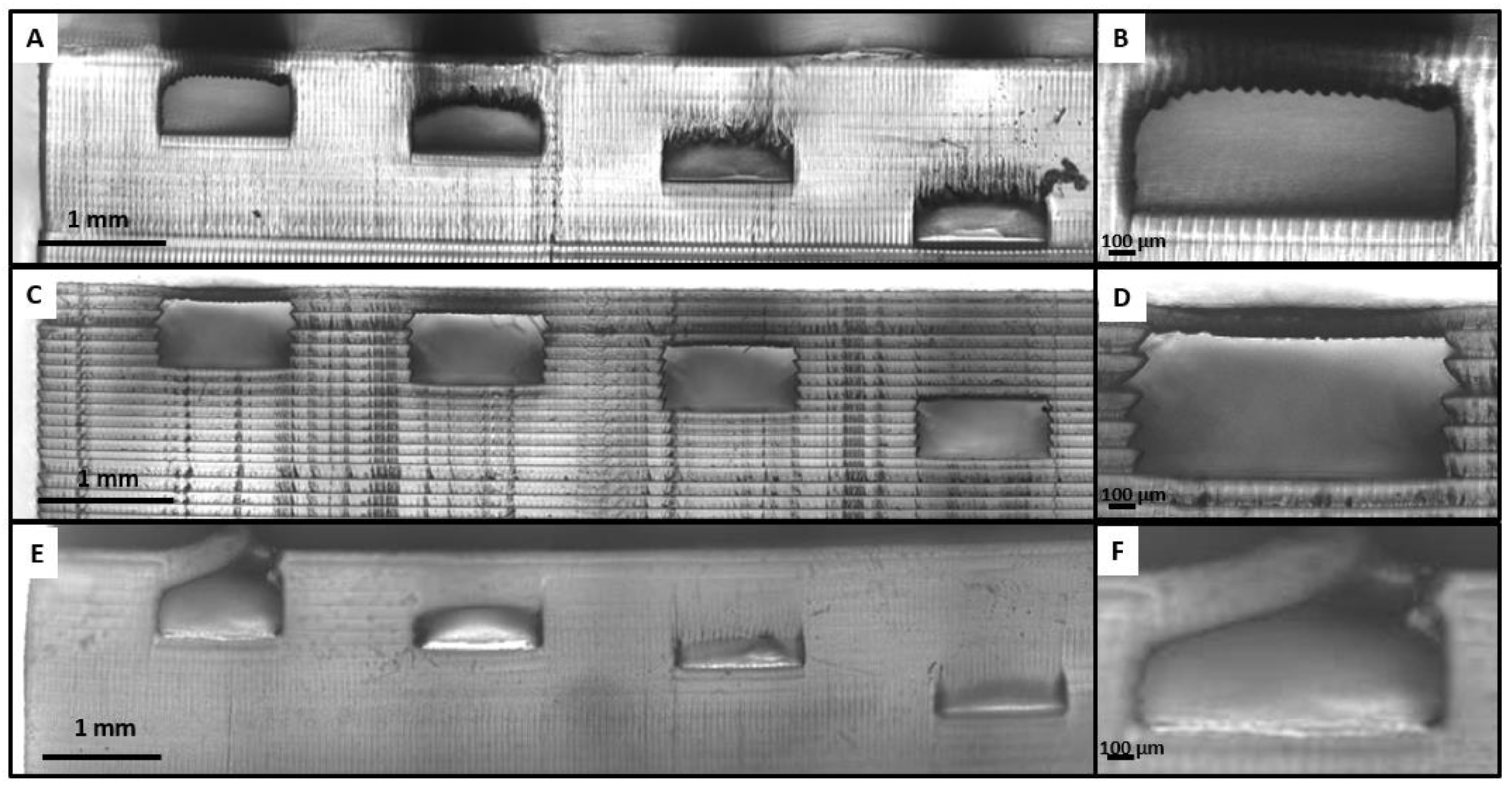
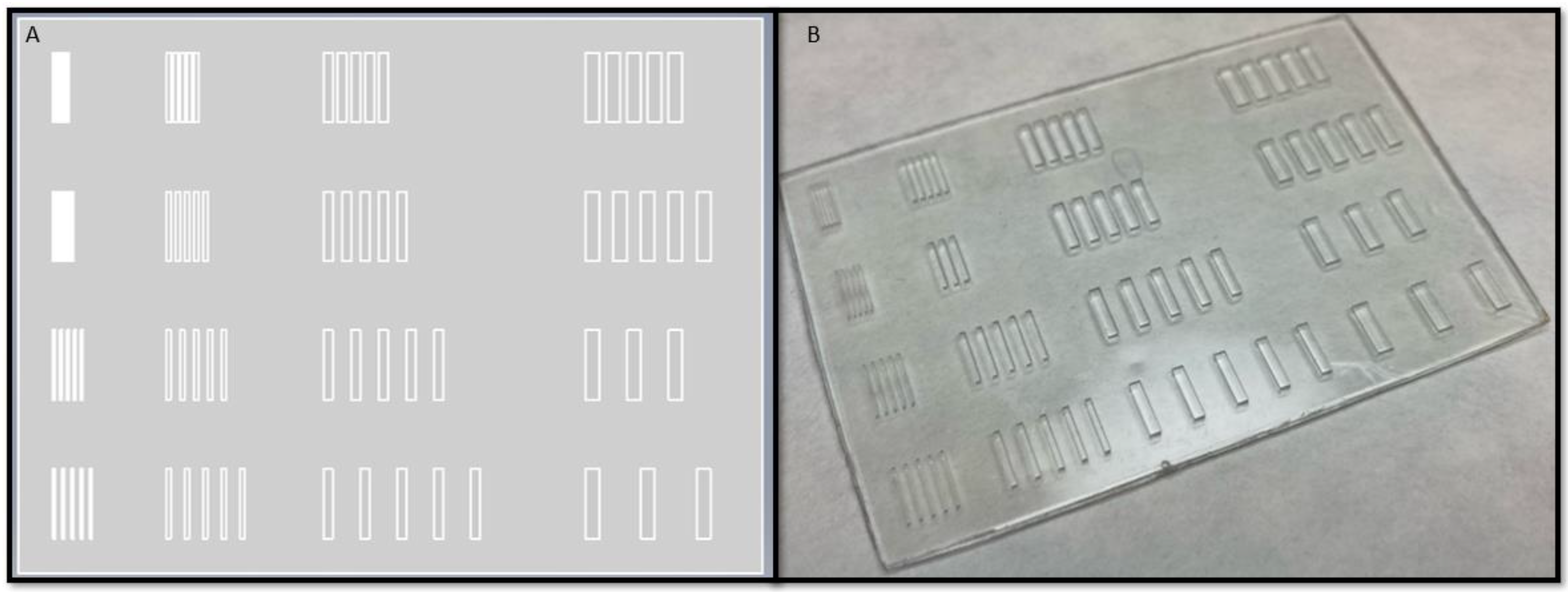
3.2. Width Dimensioning
3.3. Z Dimensioning
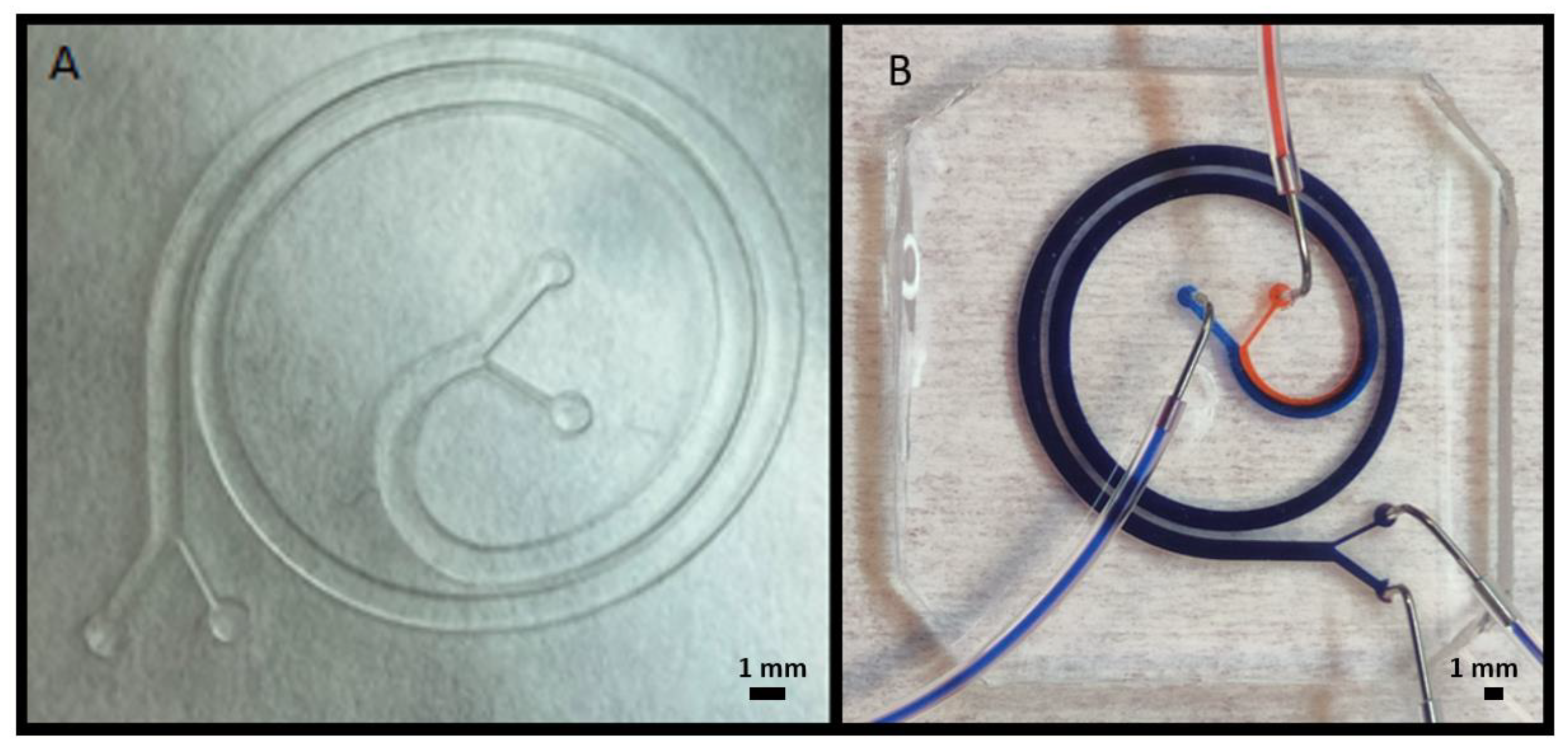
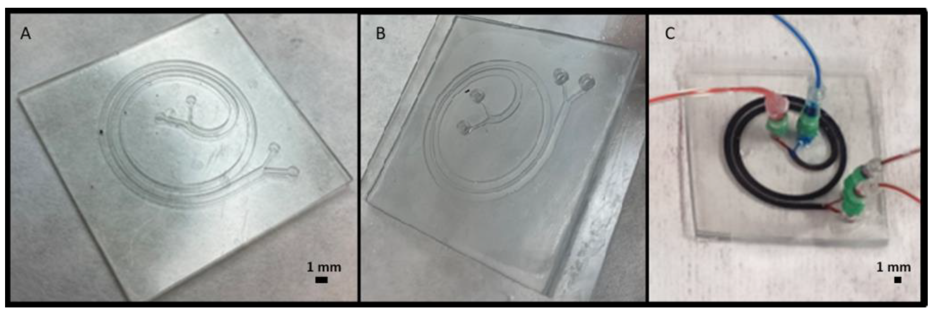
3.4. Microfluidic Devices Fabrication Using 3D Printed Molds or Assembling 3D Printed Parts
3.5. Microfluidic Devices Fabrication in One-Step
4. Discussion
5. Conclusions
Author Contributions
Funding
Institutional Review Board Statement
Informed Consent Statement
Data Availability Statement
Acknowledgments
Conflicts of Interest
Appendix A

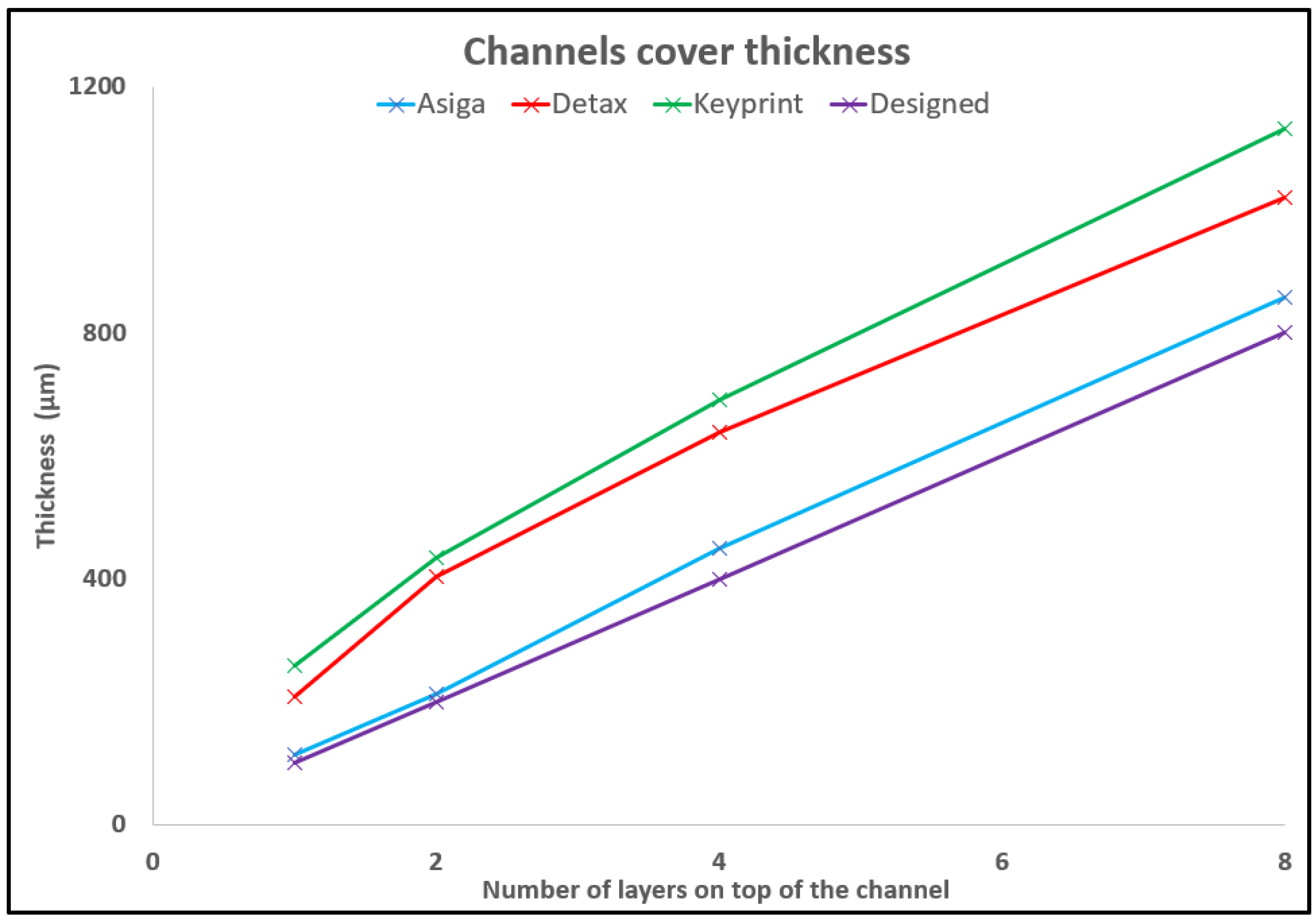
| Resin\Number of Layers | 1 | 2 | 4 | 8 |
|---|---|---|---|---|
| Asiga | 114.5 | 212.3 | 448.9 | 857.6 |
| Detax | 207.2 | 404.2 | 637.4 | 1019.6 |
| Keyprint | 259.1 | 435.0 | 690.4 | 1131.8 |
| Designed | 100.0 | 200.0 | 400.0 | 800.0 |
Appendix B

References
- Whitesides, G.M. The origins and the future of microfluidics. Nature 2006, 442, 368–373. [Google Scholar] [CrossRef] [PubMed]
- Gale, B.K.; Jafek, A.R.; Lambert, C.J.; Goenner, B.L.; Moghimifam, H.; Nze, U.C.; Kamarapu, S.K. A Review of Current Methods in Microfluidic Device Fabrication and Future Commercialization Prospects. Inventions 2018, 3, 60. [Google Scholar] [CrossRef] [Green Version]
- Bhattacharjee, N.; Urrios, A.; Kang, S.; Folch, A. The upcoming 3D-printing revolution in microfluidics. Lab Chip 2016, 16, 1720–1742. [Google Scholar] [CrossRef] [Green Version]
- Au, A.K.; Huynh, W.; Horowitz, L.F.; Folch, A. 3D-Printed Microfluidics. Angew. Chem. Int. Ed. 2016, 55, 3862–3881. [Google Scholar] [CrossRef] [PubMed]
- Li, F.; Macdonald, N.P.; Guijt, R.M.; Breadmore, M.C. Increasing the functionalities of 3D printed microchemical devices by single material, multimaterial, and print-pause-print 3D printing. Lab Chip 2019, 19, 35–49. [Google Scholar] [CrossRef] [PubMed] [Green Version]
- Waheed, S.; Cabot, J.M.; Macdonald, N.P.; Lewis, T.; Guijt, R.M.; Paull, B.; Breadmore, M.C. 3D printed microfluidic devices: Enablers and barriers. Lab Chip 2016, 16, 1993–2013. [Google Scholar] [CrossRef] [PubMed] [Green Version]
- Hull, C. StereoLithography: Plastic prototypes from CAD data without tooling. Mod. Cast. 1988, 78, 38. [Google Scholar]
- Crump, S.S. Apparatus and Method for Creating Three-Dimensional Objects. U.S. Patent No. 5,121,329, 9 June 1992. [Google Scholar]
- Eng, H.; Maleksaeedi, S.; Yu, S.; Choong, Y.; Wiria, F.; Tan, C.; Su, P.; Wei, J. 3D Stereolithography of Polymer Composites Reinforced with Orientated Nanoclay. Procedia Eng. 2017, 216, 1–7. [Google Scholar] [CrossRef]
- Kuo, A.P.; Bhattacharjee, N.; Lee, Y.; Castro, K.; Kim, Y.T.; Folch, A. High-Precision Stereolithography of Biomicrofluidic Devices. Adv. Mater. Technol. 2019, 4, 1800395. [Google Scholar] [CrossRef]
- Beauchamp, M.J.; Gong, H.; Woolley, A.T.; Nordin, G.P. 3D Printed Microfluidic Features Using Dose Control in X, Y, and Z Dimensions. Micromachines 2018, 9, 326. [Google Scholar] [CrossRef] [Green Version]
- Kardar, P.; Ebrahimi, M.; Bastani, S. Influence of temperature and light intensity on the photocuring process and kinetics parameters of a pigmented UV curable system. J. Therm. Anal. 2014, 118, 541–549. [Google Scholar] [CrossRef]
- Au, A.K.; Lee, W.; Folch, A. Mail-order microfluidics: Evaluation of stereolithography for the production of microfluidic devices. Lab Chip 2014, 14, 1294–1301. [Google Scholar] [CrossRef] [PubMed] [Green Version]
- O’Neill, P.F.; Kent, N.; Brabazon, D.; Neill PF, O.; Kent, N.; Brabazon, D. Mitigation and control of the overcuring effect in mask projection micro-stereolithography. AIP Publ. LLC 2017, 1896, 200012. [Google Scholar] [CrossRef] [Green Version]
- Macdonald, N.P.; Cabot, J.M.; Smejkal, P.; Guijt, R.M.; Paull, B.; Breadmore, M.C. Comparing Microfluidic Performance of Three-Dimensional (3D) Printing Platforms. Anal. Chem. 2017, 89, 3858–3866. [Google Scholar] [CrossRef]
- Enders, A.; Siller, I.G.; Urmann, K.; Hoffmann, M.R.; Bahnemann, J. 3D Printed Microfluidic Mixers—A Comparative Study on Mixing Unit Performances. Small 2019, 15, e1804326. [Google Scholar] [CrossRef] [Green Version]
- Bazaz, S.R.; Rouhi, O.; Raoufi, M.A.; Ejeian, F.; Asadnia, M.; Jin, D.; Warkiani, M.E. 3D Printing of Inertial Microfluidic Devices. Sci. Rep. 2020, 10, 5929. [Google Scholar] [CrossRef] [Green Version]
- Detax. Available online: https://www.detax.de/en/shop/produkte/Freeprint-ortho.php (accessed on 21 January 2022).
- Keyprint. Available online: https://keyprint.keystoneindustries.com/keyortho-ibt/ (accessed on 21 January 2022).
- Asiga. Available online: https://www.asiga.com/products/materials/ (accessed on 21 January 2022).
- Horcas, I.; Fernández, R.; Gómez-Rodriguez, J.M.; Colchero, J.; Gomez-Herrero, J.; Baro, A.M. WSXM: A software for scanning probe microscopy and a tool for nanotechnology. Rev. Sci. Instrum. 2007, 78, 13705. [Google Scholar] [CrossRef] [PubMed]
- Mostafa, K.G.; Nobes, D.S.; Qureshi, A.J. Investigation of Light-Induced Surface Roughness in Projection Micro-ScienceDirect Investigation of Light-Induced Surface Roughness in Projection Micro- Stereolithography Additive Manufacturing (PµSLA). Procedia CIRP 2020, 92, 187–193. [Google Scholar] [CrossRef]
- Di Carlo, D. Inertial microfluidics. Lab Chip 2009, 9, 3038–3046. [Google Scholar] [CrossRef]
- Hou, H.W.; Warkiani, M.E.; Khoo, B.L.; Li, Z.R.; Soo, R.A.; Tan, D.S.-W.; Lim, W.-T.; Han, J.; Bhagat, A.A.S.; Lim, C.T. Isolation and retrieval of circulating tumor cells using centrifugal forces. Sci. Rep. 2013, 3, 1259. [Google Scholar] [CrossRef] [Green Version]
- Zhou, Y. Balance between bonding and deposition during fused deposition modeling of polycarbonate and acrylonitrile-butadiene-styrene composites. Polym. Compos. 2019, 41, 60–72. [Google Scholar] [CrossRef]


| Variable | Detax | Asiga | Keyprint |
|---|---|---|---|
| Exposure time for burn in layer (s) | 6 | 40 | 7 |
| Exposure time for normal layer (s) | 2 | 20 | 4 |
| Layer thickness (µm) | 100 | 100 | 100 |
| Light power (PWM) | 35 | 35 | 35 |
| Resin | Designed Height (µm) | Average Height Error |
|---|---|---|
| Detax | 600 | 7.14% |
| 400 | 9.35% | |
| 200 | 22.32% | |
| Asiga | 600 | 16.73% |
| 400 | 17.39% | |
| 200 | 27.25% | |
| Keyprint | 600 | 34.43% |
| 400 | 46.38% |
| Resin | Feature Type | Width Error | Height Error |
|---|---|---|---|
| Detax | Extrusion | 0.14% | 0.94% |
| Embossed | 0.30% | 3.62% | |
| Asiga | Extrusion | 0.24% | 0.93% |
| Embossed | 0.31% | 4.98% | |
| Keyprint | Extrusion | 0.34% | 3.40% |
| Embossed | 1.43% | 4.67% |
Publisher’s Note: MDPI stays neutral with regard to jurisdictional claims in published maps and institutional affiliations. |
© 2022 by the authors. Licensee MDPI, Basel, Switzerland. This article is an open access article distributed under the terms and conditions of the Creative Commons Attribution (CC BY) license (https://creativecommons.org/licenses/by/4.0/).
Share and Cite
Subirada, F.; Paoli, R.; Sierra-Agudelo, J.; Lagunas, A.; Rodriguez-Trujillo, R.; Samitier, J. Development of a Custom-Made 3D Printing Protocol with Commercial Resins for Manufacturing Microfluidic Devices. Polymers 2022, 14, 2955. https://doi.org/10.3390/polym14142955
Subirada F, Paoli R, Sierra-Agudelo J, Lagunas A, Rodriguez-Trujillo R, Samitier J. Development of a Custom-Made 3D Printing Protocol with Commercial Resins for Manufacturing Microfluidic Devices. Polymers. 2022; 14(14):2955. https://doi.org/10.3390/polym14142955
Chicago/Turabian StyleSubirada, Francesc, Roberto Paoli, Jessica Sierra-Agudelo, Anna Lagunas, Romen Rodriguez-Trujillo, and Josep Samitier. 2022. "Development of a Custom-Made 3D Printing Protocol with Commercial Resins for Manufacturing Microfluidic Devices" Polymers 14, no. 14: 2955. https://doi.org/10.3390/polym14142955
APA StyleSubirada, F., Paoli, R., Sierra-Agudelo, J., Lagunas, A., Rodriguez-Trujillo, R., & Samitier, J. (2022). Development of a Custom-Made 3D Printing Protocol with Commercial Resins for Manufacturing Microfluidic Devices. Polymers, 14(14), 2955. https://doi.org/10.3390/polym14142955