
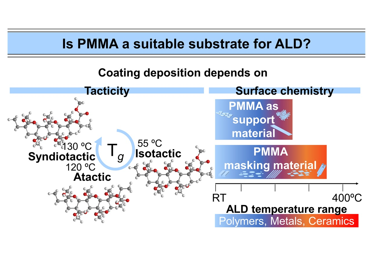
Is Poly(methyl methacrylate) (PMMA) a Suitable Substrate for ALD?: A Review

 , ,
, ,  and
and
Abstract
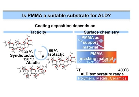
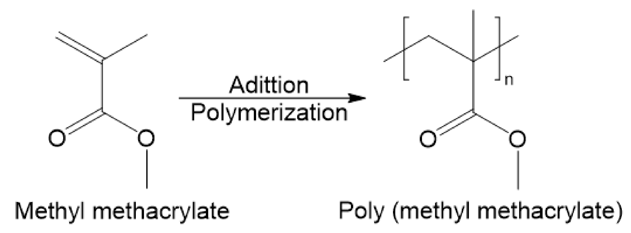
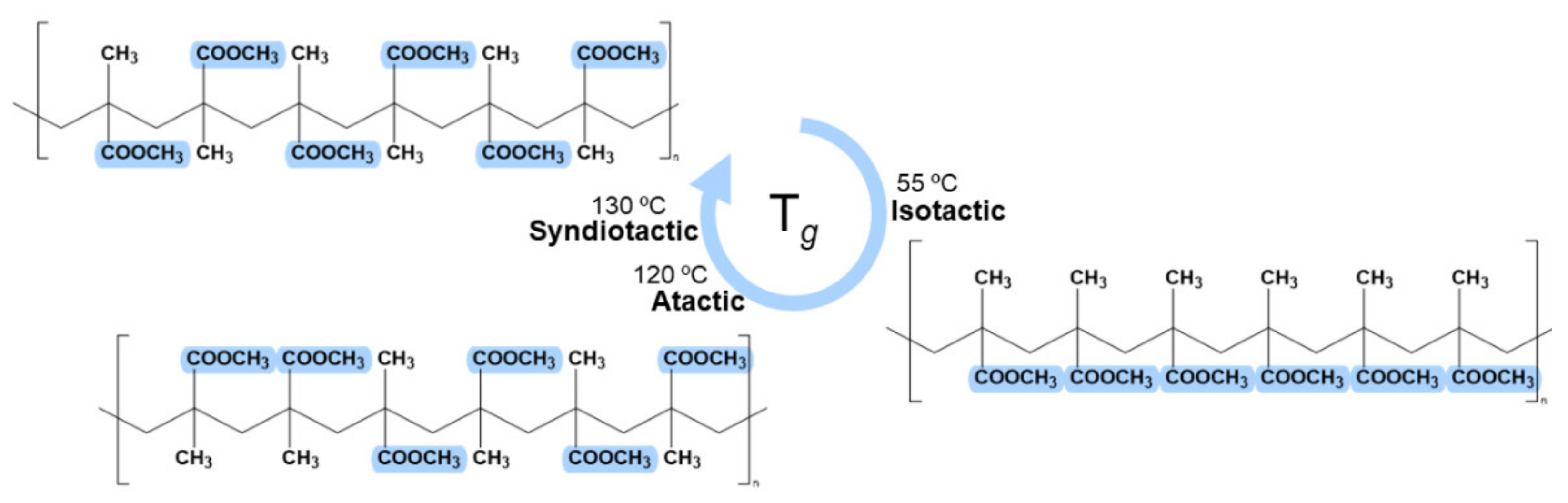
1. Introduction
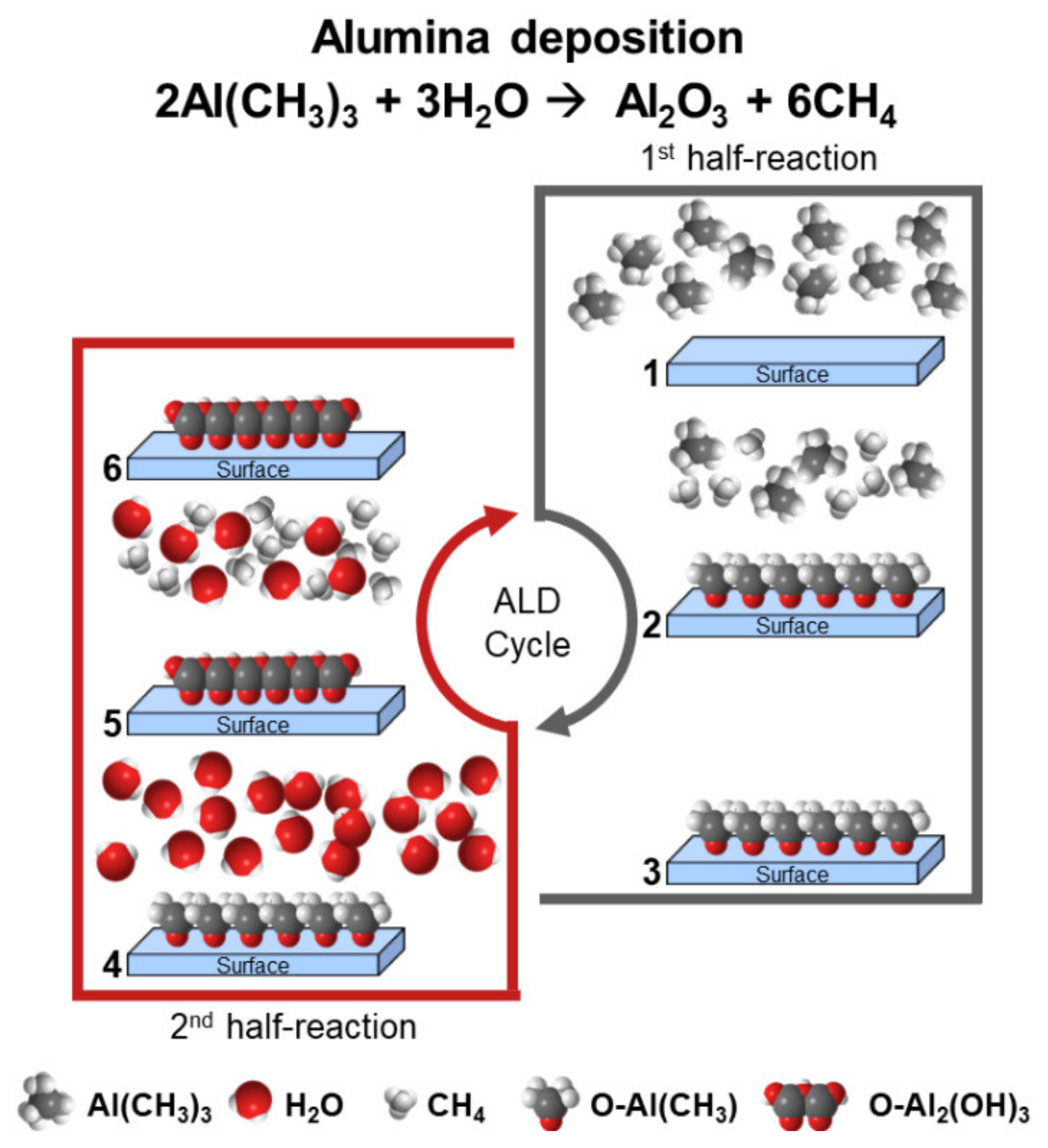
2. Brief History of Atomic Layer Deposition
3. Coatings on PMMA by Thermal Atomic Layer Deposition
3.1. PMMA Challenges for ALD
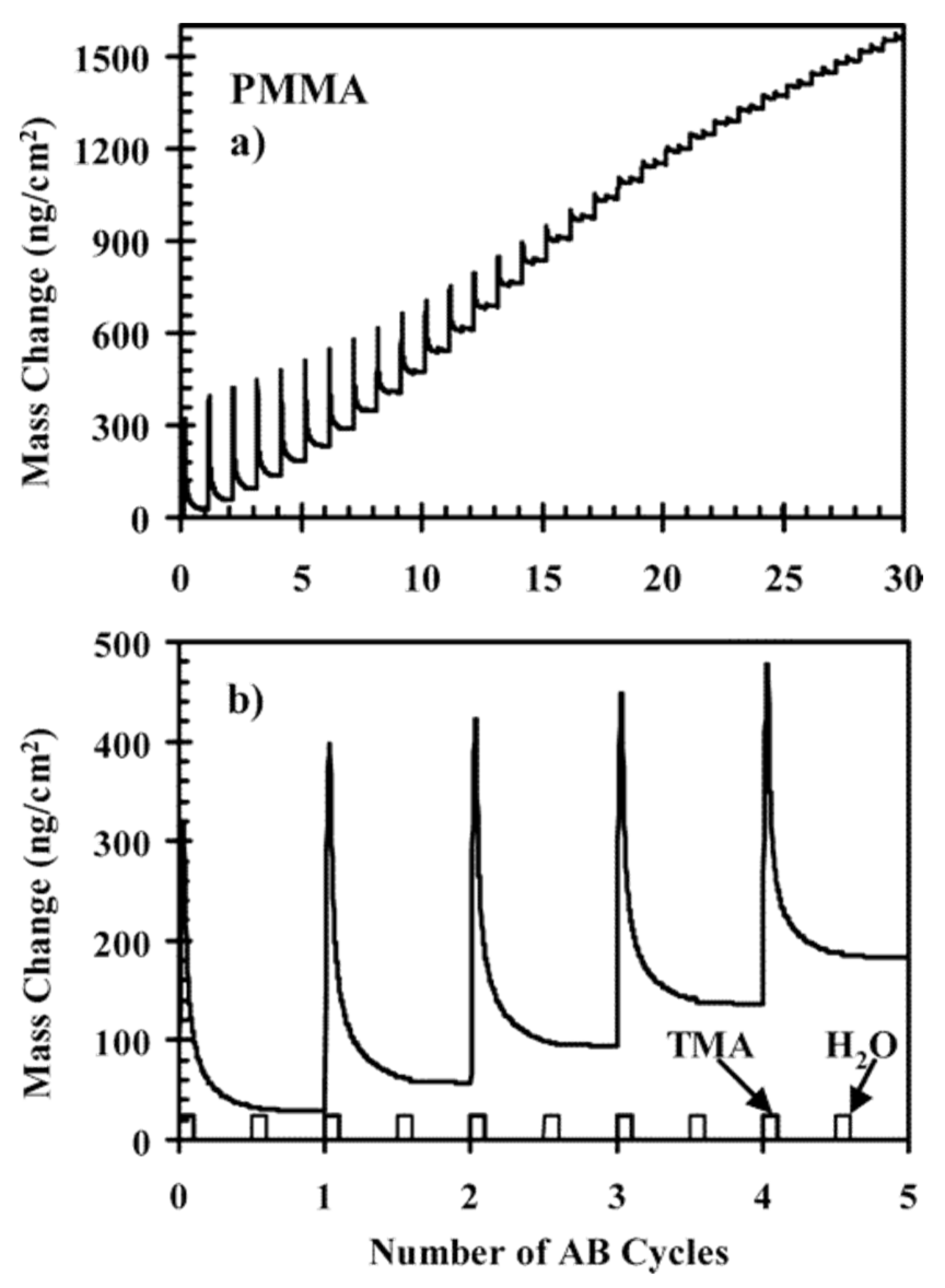
3.2. Nucleation and Growth Studies
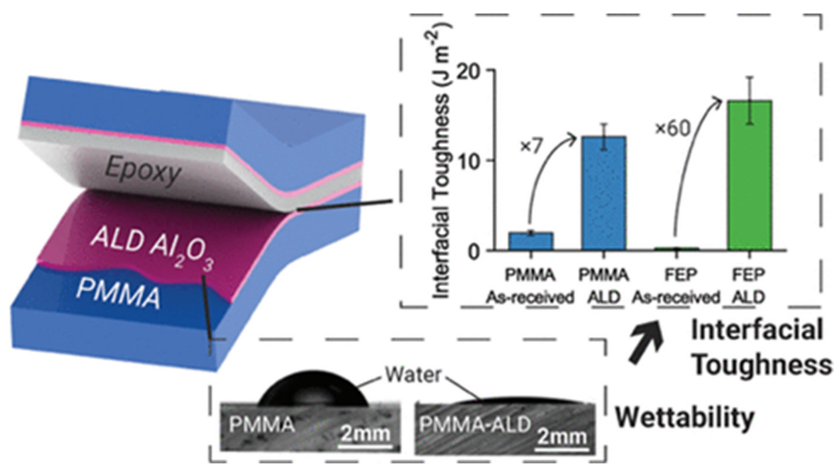
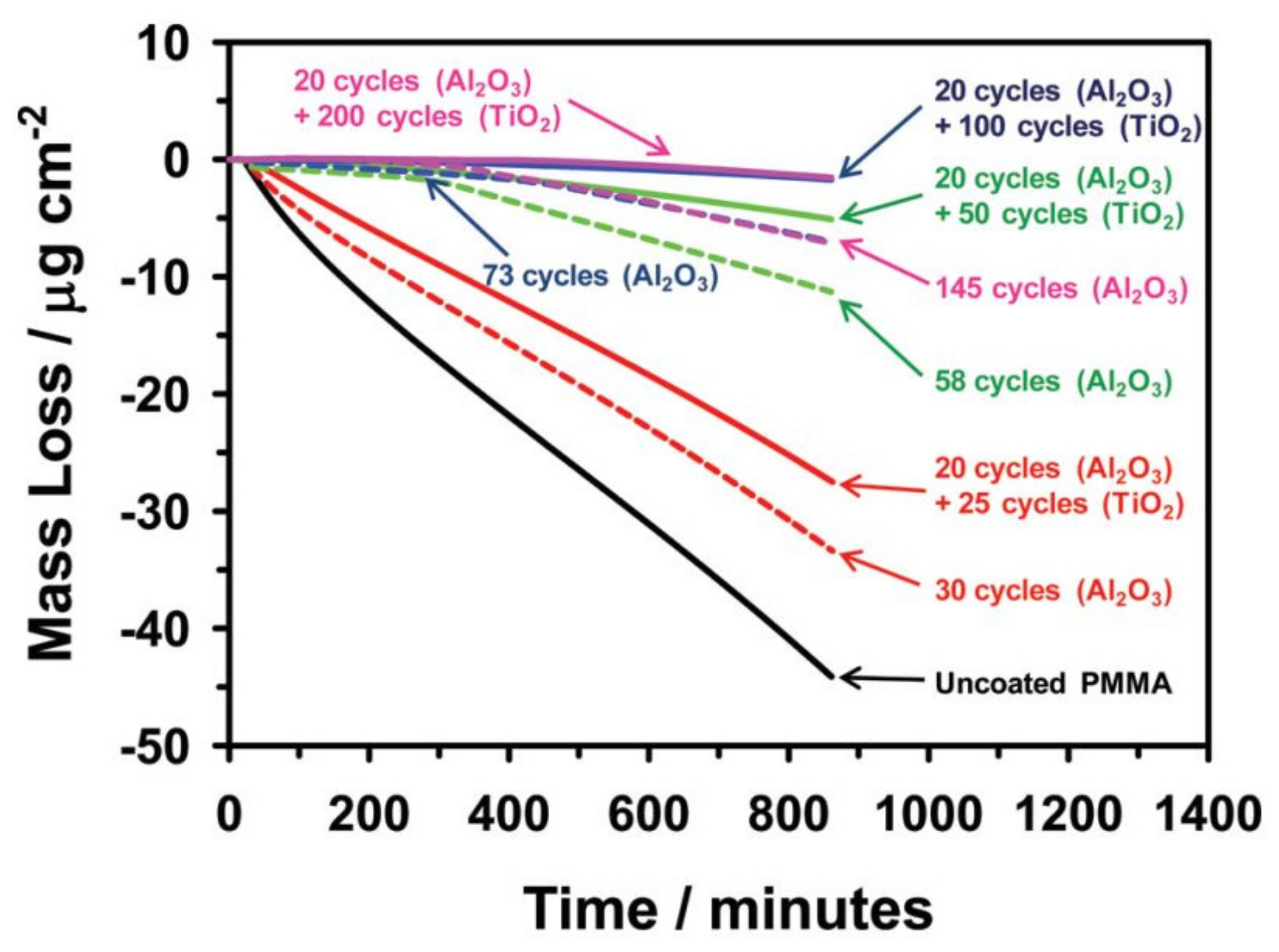
3.3. Adhesion and Mechanical Properties
3.4. Applications
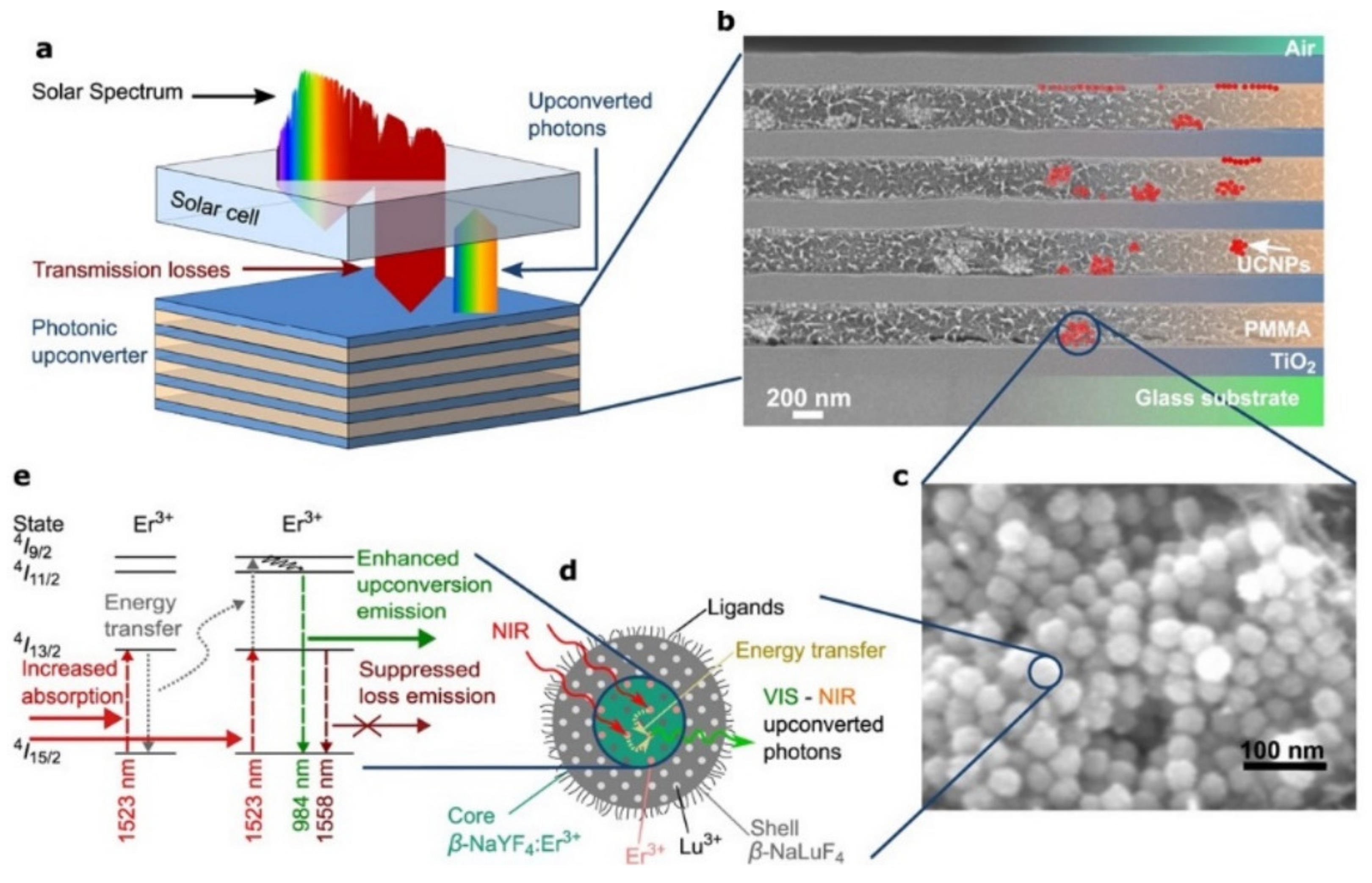
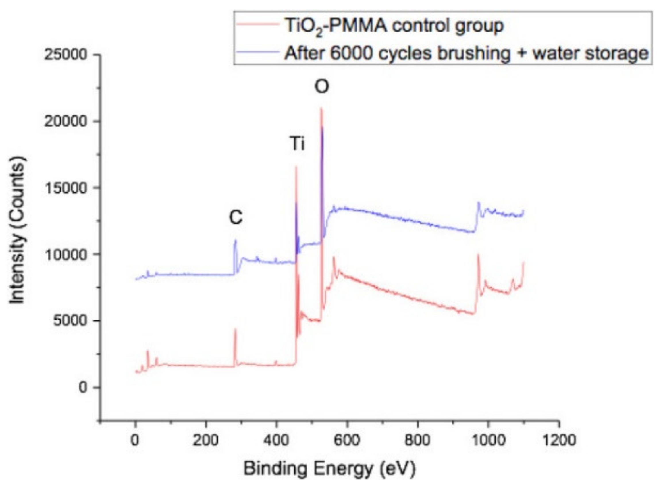
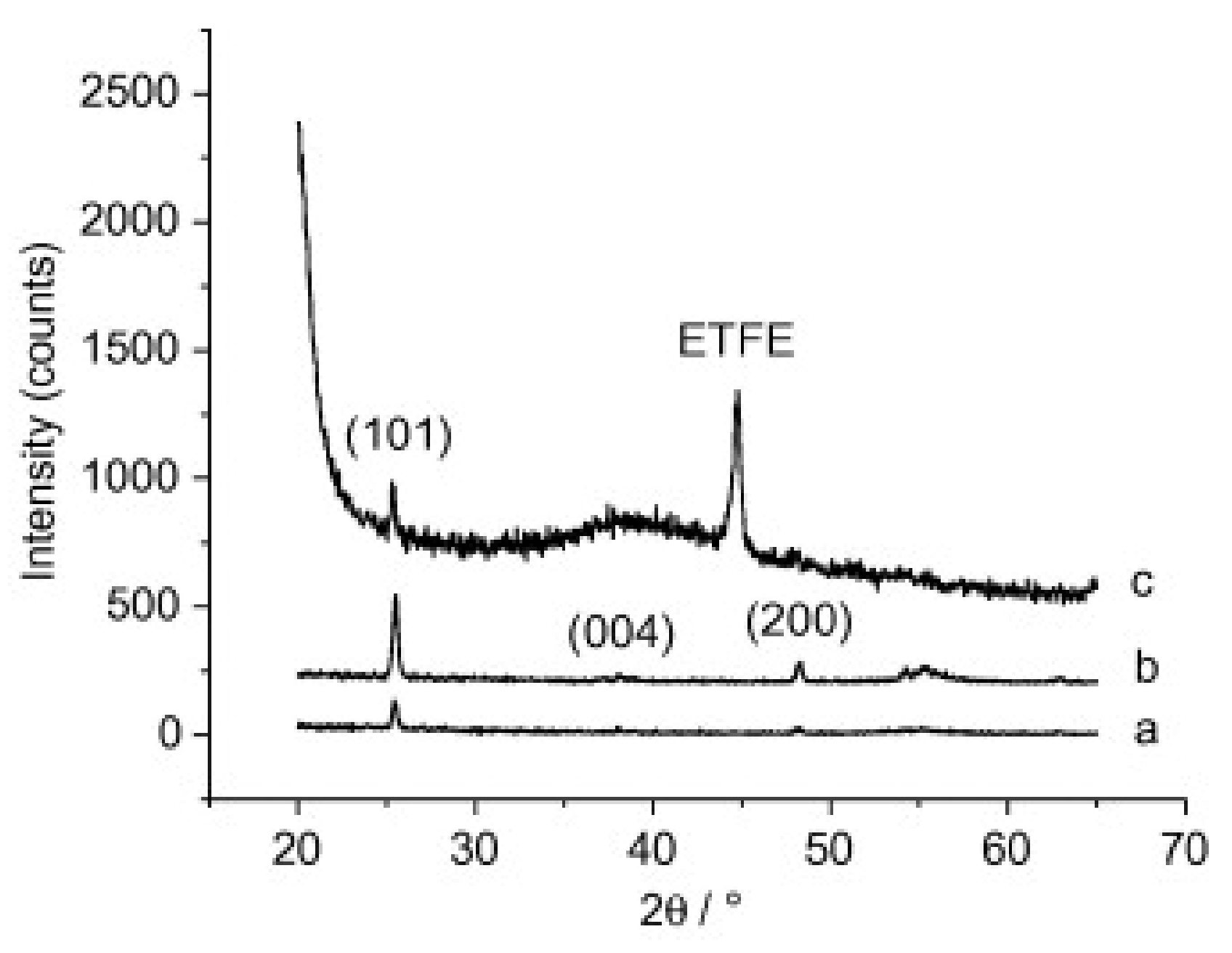
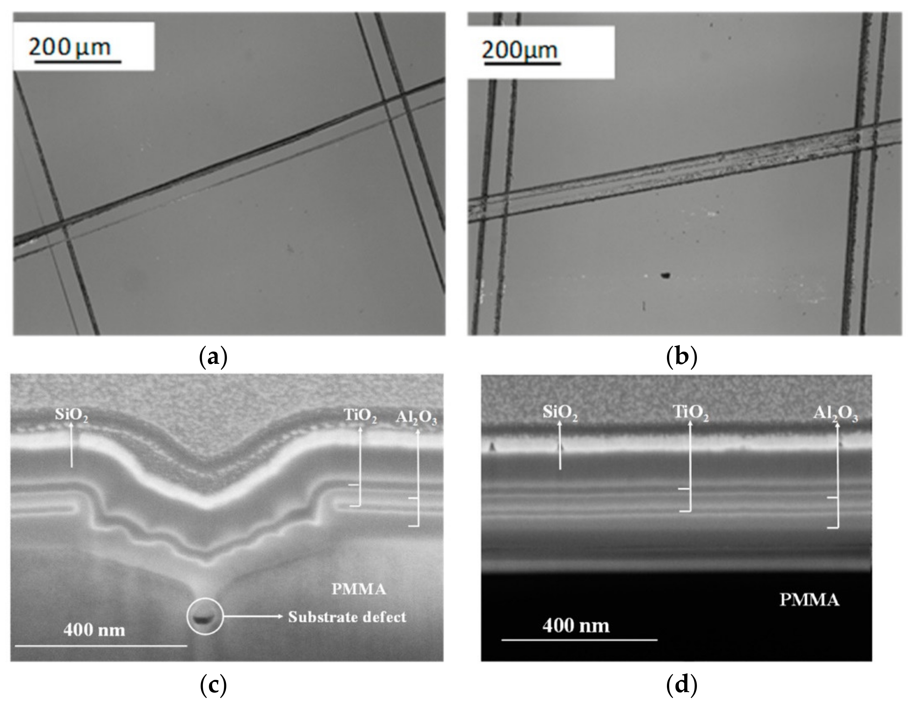
3.4.1. Applications in Photonics, Photoluminescence, and Photocatalysis
3.4.2. Applications in Dentistry
4. ALD Coatings on PMMA Aided by Seed Layer
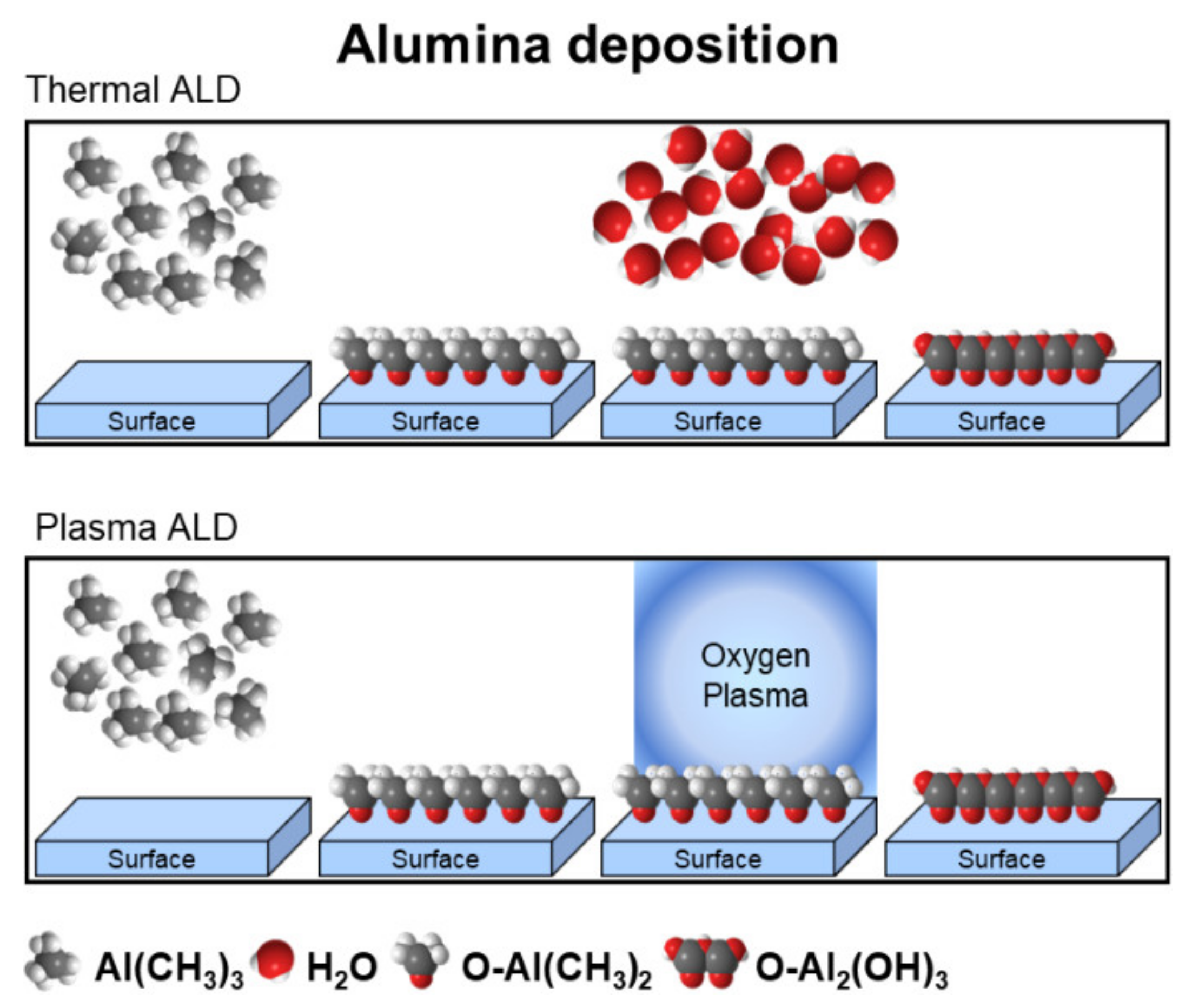
5. Coatings on PMMA by Plasma Atomic Layer Deposition
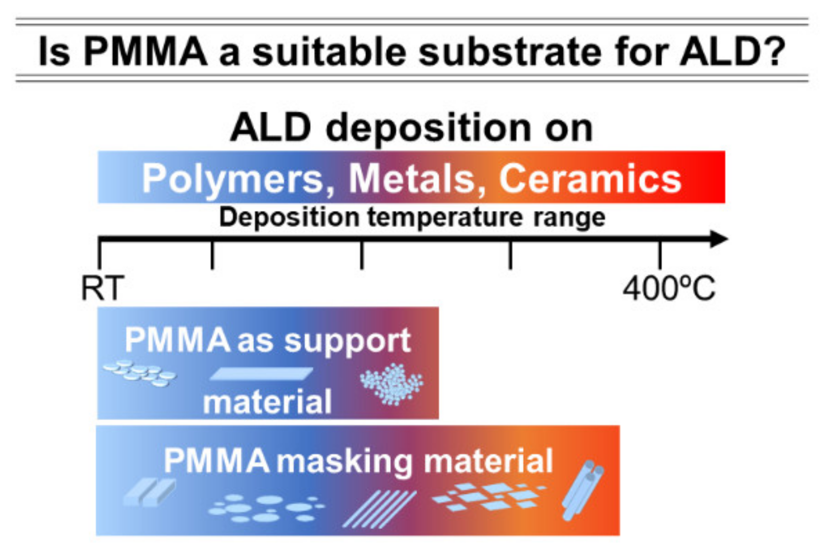
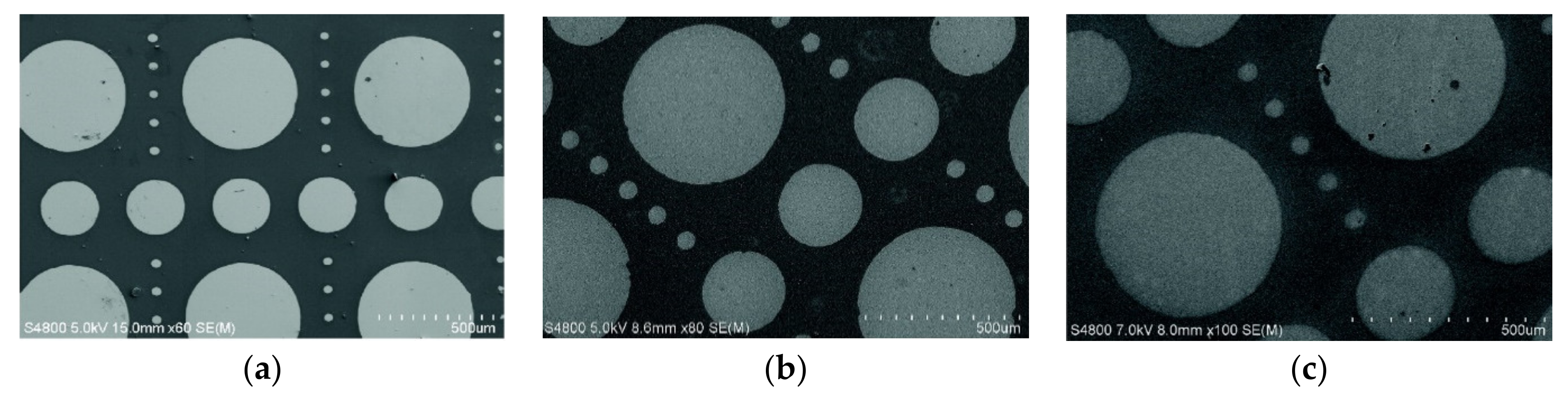
6. Area Selective ALD on PMMA
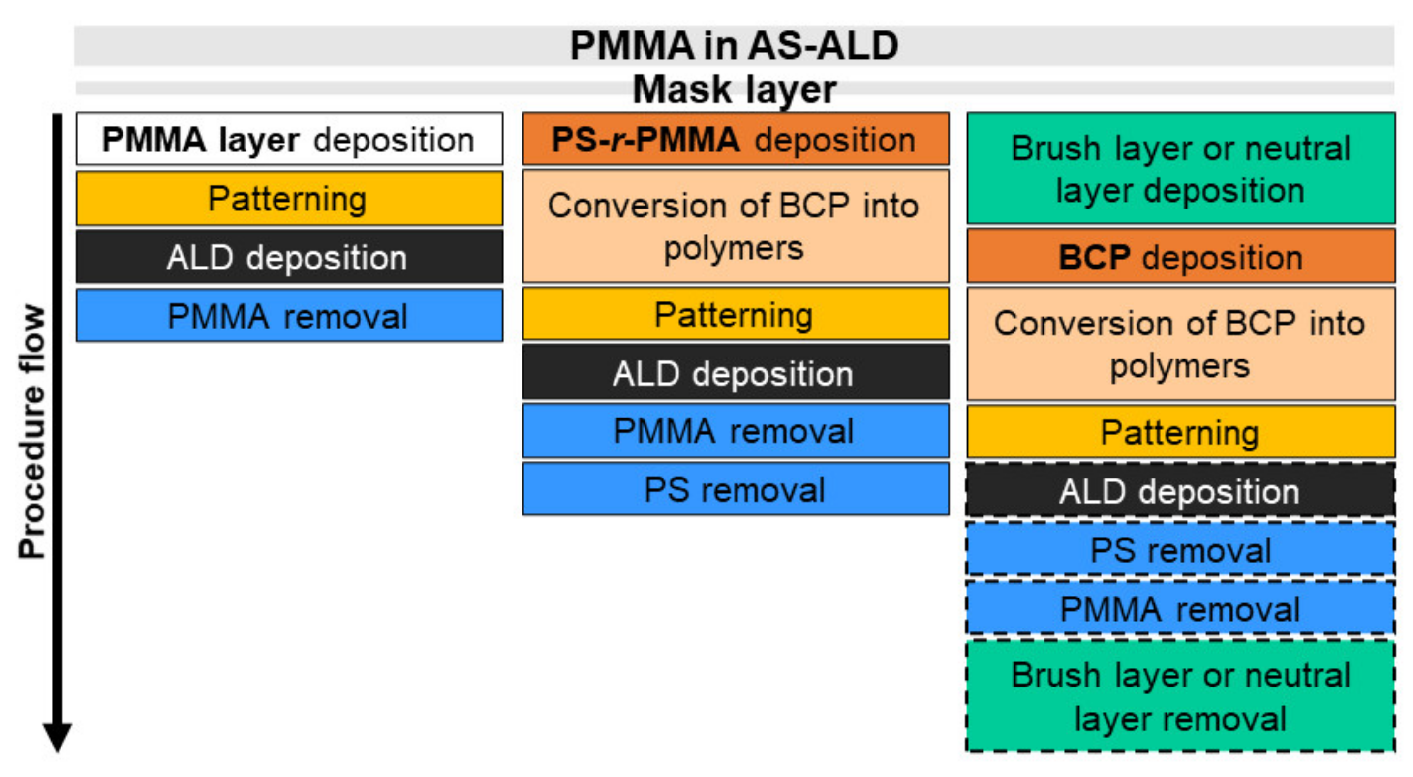
6.1. PMMA as Masking Layer
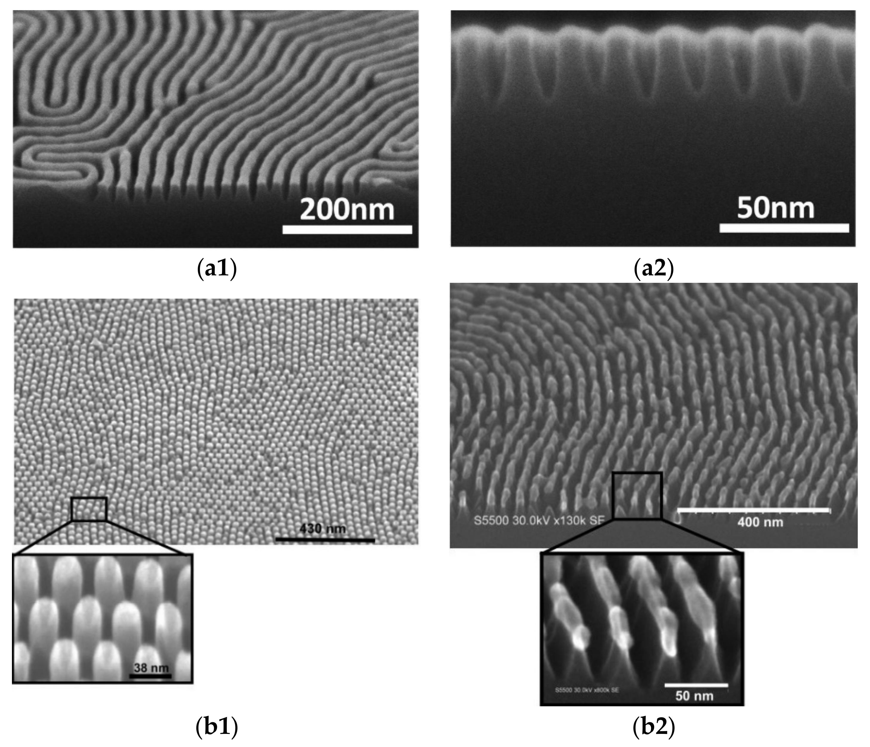
6.2. ALD on Di-Block Copolymer Masks
7. Summary and Prospective
Author Contributions
Funding
Institutional Review Board Statement
Informed Consent Statement
Data Availability Statement
Acknowledgments
Conflicts of Interest
References
- Goseki, R.; Ishizone, T. Poly(methyl methacrylate) (PMMA). Encycl. Polym. Nanomater. 2014, 1–11. [Google Scholar] [CrossRef]
- Hu, L.; Yang, Z.; Zhang, X.; Liu, Z.; Xia, P.; Deng, K.; Gong, L.; Jiang, L.; Zhang, H. Fabrication and evaluation of dual function PMMA/nano-carbon composite particles for UV curable anti-glare coating. Prog. Org. Coat. 2016, 101, 81–89. [Google Scholar] [CrossRef]
- Van Krevelen, D.W. Properties of Polymers: Their Correlation with Chemical Structure; Their Numerical Estimation and Prediction from Additive Group Contributions, 4th ed.; Nijenhuis, K., Ed.; Elsevier Publications: Amsterdam, The Netherlands, 2000; ISBN 9780080548197. [Google Scholar]
- Shah, J.J.; Geist, J.; Locascio, L.E.; Gaitan, M.; Rao, M.V.; Vreeland, W.N. Surface modification of poly(methyl methacrylate) for improved adsorption of wall coating polymers for microchip electrophoresis. Electrophoresis 2006, 27, 3788–3796. [Google Scholar] [CrossRef] [PubMed]
- Peters, E.N. Thermoplastics, Thermosets, and Elastomers—Descriptions and Properties. In Mechanical Engineers’ Handbook; Kutz, M., Ed.; John Wiley & Sons, Inc.: Hoboken, NJ, USA; SABIC: Selkirk, NY, USA, 2015; pp. 1–48. ISBN 9781118985960. [Google Scholar]
- Sharif, M.M.; Johari, M.A.M.; Al Noman, A.; Abdul Khudus, M.I.M.; Harun, S.W. PMMA microfiber and Microball Resonator for fomaldehyde liquid sensing. Sens. Actuators A Phys. 2020, 304, 111828. [Google Scholar] [CrossRef]
- Al-Nemrawi, N.K.; Marques, J.; Tavares, C.J.; Oweis, R.J.; Al-Fandi, M.G. Synthesis and characterization of photocatalytic polyurethane and poly(methyl methacrylate) microcapsules for the controlled release of methotrexate. Drug Dev. Ind. Pharm. 2018, 44, 2083–2088. [Google Scholar] [CrossRef]
- Alves Batista, F.; Brena Cunha Fontele, S.; Beserra Santos, L.K.; Alves Filgueiras, L.; Quaresma Nascimento, S.; de Castro e Sousa, J.M.; Ramos Gonçalves, J.C.; Nogueira Mendes, A. Synthesis, characterization of α-terpineol-loaded PMMA nanoparticles as proposed of therapy for melanoma. Mater. Today Commun. 2020, 22. [Google Scholar] [CrossRef]
- Li, X.; Li, D.; Liu, X.; Chang, H. Ultra-monodisperse droplet formation using PMMA microchannels integrated with low-pulsation electrolysis micropumps. Sens. Actuators B Chem. 2016, 229, 466–475. [Google Scholar] [CrossRef]
- Deepa, M.; Sharma, N.; Agnihotry, S.A.; Singh, S.; Lal, T.; Chandra, R. Conductivity and viscosity of liquid and gel electrolytes based on LiClO4, LiN(CF3SO2)2 and PMMA. Solid State Ionics 2002, 152–153, 253–258. [Google Scholar] [CrossRef]
- Devikala, S.; Kamaraj, P.; Arthanareeswari, M. AC conductivity studies of PMMA/TiO2 composites. Mater. Today Proc. 2018, 5, 8678–8682. [Google Scholar] [CrossRef]
- Ko, Y.; Kim, Y.; Lee, C.; Kim, Y.; Jun, Y. Poly(methyl methacrylate) embedded perovskite films for improving solar cell performance. Synth. Met. 2019, 249, 47–51. [Google Scholar] [CrossRef]
- Alves, M.; Pérez-Rodríguez, A.; Dale, P.J.; Domínguez, C.; Sadewasser, S. Thin-film micro-concentrator solar cells. J. Phys. Energy 2019, 2, 012001. [Google Scholar] [CrossRef]
- Loffredo, F.; Villani, F.; Cancro, C.; Nenna, G.; Borriello, A.; Miscioscia, R.; Minarini, C.; Roca, F. Evaluation of the PMMA microlens efficiency for the realization of a solar micro-concentrator array. Appl. Opt. 2018, 57, 4396. [Google Scholar] [CrossRef]
- Fujimoto, K.; Tadokoro, H.; Ueda, Y.; Ikada, Y. Polyurethane surface modification by graft polymerization of acrylamide for reduced protein adsorption and platelet adhesion. Biomaterials 1993, 14, 442–448. [Google Scholar] [CrossRef]
- Torstensson, M.; Ranby, B.; Hult, A. Monomeric Surfactants for Surface Modification of Polymers. Macromolecules 1990, 23, 126–132. [Google Scholar] [CrossRef]
- Pinna, N.; Knez, M. Atomic Layer Deposition of Nanotructured Materials, 1st ed.; Pinna, N., Knez, M., Eds.; Wiley-VCH Verlag & Co. KGaA: Weinheim, Germany, 2011; ISBN 9780470109526. [Google Scholar]
- Knez, M.; Nielsch, K.; Niinistö, L. Synthesis and Surface Engineering of Complex Nanostructures by Atomic Layer Deposition. Adv. Mater. 2007, 19, 3425–3438. [Google Scholar] [CrossRef]
- Miikkulainen, V.; Leskelä, M.; Ritala, M.; Puurunen, R.L. Crystallinity of inorganic films grown by atomic layer deposition: Overview and general trends. J. Appl. Phys. 2013, 113. [Google Scholar] [CrossRef]
- Parsons, G.N.; Elam, J.W.; George, S.M.; Haukka, S.; Jeon, H.; (Erwin) Kessels, W.M.M.; Leskelä, M.; Poodt, P.; Ritala, M.; Rossnagel, S.M. History of atomic layer deposition and its relationship with the American Vacuum Society. J. Vac. Sci. Technol. A Vac. Surf. Film. 2013, 31, 050818. [Google Scholar] [CrossRef]
- George, S.M. Atomic Layer Deposition: An Overview. Chem. Rev. 2010, 110, 111–131. [Google Scholar] [CrossRef] [PubMed]
- Puurunen, R.L. Surface chemistry of atomic layer deposition: A case study for the trimethylaluminum/water process. J. Appl. Phys. 2005, 97, 121301. [Google Scholar] [CrossRef]
- French, P.; Krijnen, G.; Roozeboom, F. Precision in harsh environments. Microsyst. Nanoeng. 2016, 2, 16048. [Google Scholar] [CrossRef]
- Leskelä, M.; Ritala, M. Atomic Layer Deposition Chemistry: Recent Developments and Future Challenges. Angew. Chem. Int. Ed. 2003, 42, 5548–5554. [Google Scholar] [CrossRef] [PubMed]
- Niinistö, L.; Nieminen, M.; Päiväsaari, J.; Niinistö, J.; Putkonen, M.; Nieminen, M. Advanced electronic and optoelectronic materials by Atomic Layer Deposition: An overview with special emphasis on recent progress in processing of high-k dielectrics and other oxide materials. Phys. Status Solidi 2004, 201, 1443–1452. [Google Scholar] [CrossRef]
- Muñoz-Rojas, D.; MacManus-Driscoll, J. Spatial atmospheric atomic layer deposition: A new laboratory and industrial tool for low-cost photovoltaics. Mater. Horiz. 2014, 1, 314–320. [Google Scholar] [CrossRef]
- Knoops, H.C.M.; Potts, S.E.; Bol, A.A.; Kessels, W.M.M. Atomic Layer Deposition. In Handbook of Crystal Growth: Thin Films and Epitaxy, 2nd ed.; Kuech, T.F., Ed.; Elsevier B.V.: Eindhoven, The Netherlands, 2015; Volume 3, pp. 1101–1134. ISBN 9780444633057. [Google Scholar]
- Aleskovskii, V.B.; Koltsov, S.I. Some characteristics of molecular layering reactions. In Proceedings of the Abstract of Scientific and Technical Conference of the Leningrad Technological Institute by Lensovet, Goskhimizdat, Leningrad, 26–29 November 1965; p. 67. [Google Scholar]
- Sveshnikova, G.V.; Koltsov, S.I.; Aleskovskii, V.B. Interaction of titanium tetrachloride with hydroxylated silicon surfaces. J. Appl. Chem. USSR 1970, 43, 432–434. [Google Scholar]
- Sveshnikova, G.V.; Koltsov, S.I.; Aleskovskii, A.B. Measuring thicknesses of ultra-thin silicon oxide films deposited by molecular layering on the surface of single crystal silicon using polarization method. In Proceedings of the Abstract of Scientific and Technical Conference of the Leningrad Technological Institute by Lensovet, Goskhimizdat, Leningrad; 1969; pp. 18–19. [Google Scholar]
- Suntola, T. Atomic layer epitaxy. Mater. Sci. Rep. 1989, 4, 261–312. [Google Scholar] [CrossRef]
- Ahvenniemi, E.; Akbashev, A.R.; Ali, S.; Bechelany, M.; Berdova, M.; Boyadjiev, S.; Cameron, D.C.; Chen, R.; Chubarov, M.; Cremers, V.; et al. Recommended reading list of early publications on atomic layer deposition—Outcome of the “Virtual Project on the History of ALD”. J. Vac. Sci. Technol. A Vac. Surf. Film. 2017, 35, 10801. [Google Scholar] [CrossRef]
- Suntola, T.; Antson, J. Method for producing compound thin films. US Patent 4,058,430, 15 November 1977. [Google Scholar]
- Niinistö, J.; Leskelä, M.; Ritala, M. Exhibition by the Finnish Centre of Excellence in Atomic Layer Deposition. In Proceedings of the International Baltic ALD Conference, Helsinki, Finland, 12–13 May 2014; pp. 1–31. [Google Scholar]
- Motsenyat, B.Z.; Ezhovskii, Y.K.; Levankova, L.M.; Mikhailova, N. V Formation and reactions of hydroxyl-groups on polymide surface with titanium tetrachloride. J. Appl. Chem. USSR 1984, 57, 153–155. [Google Scholar]
- Parsons, G.N.; George, S.M.; Knez, M. Progress and future directions for atomic layer deposition and ALD-based chemistry. MRS Bull. 2011, 36, 865–871. [Google Scholar] [CrossRef]
- Heil, S.B.S.S.; Van Hemmen, J.L.; van de Sanden, M.C.M.M.; Kessels, W.M.M.M. Reaction mechanisms during plasma-assisted atomic layer deposition of metal oxides: A case study for Al2O3. J. Appl. Phys. 2008, 103, 103302. [Google Scholar] [CrossRef]
- Oviroh, P.O.; Akbarzadeh, R.; Pan, D.; Coetzee, R.A.M.; Jen, T.C. New development of atomic layer deposition: Processes, methods and applications. Sci. Technol. Adv. Mater. 2019, 20, 465–496. [Google Scholar] [CrossRef]
- Pan, D.; Ma, L.; Xie, Y.; Jen, T.C.; Yuan, C. On the physical and chemical details of alumina atomic layer deposition: A combined experimental and numerical approach. J. Vac. Sci. Technol. A 2015, 33, 21511. [Google Scholar] [CrossRef]
- Wilson, C.A.; Grubbs, R.K.; George, S.M. Nucleation and growth during Al2O3 atomic layer deposition on polymers. Chem. Mater. 2005, 17, 5625–5634. [Google Scholar] [CrossRef]
- Losego, M.D.; Peng, Q. Atomic Layer Deposition and Vapor Phase Infiltration. In Surface Modification of Polymers; Pinson, J., Thiry, D., Eds.; Wiley-VCHVerlag GmbH& Co. KGaA: Weinheim, Germany, 2019; pp. 135–159. [Google Scholar]
- Ali, U.; Karim, K.J.B.A.; Buang, N.A. A Review of the Properties and Applications of Poly (Methyl Methacrylate) (PMMA). Polym. Rev. 2015, 55, 678–705. [Google Scholar] [CrossRef]
- Duval-Terrié, C.; Lebrun, L. Polymerization and characterization of PMMA: Polymer chemistry laboratory experiments for undergraduate students. J. Chem. Educ. 2006, 83, 443–446. [Google Scholar] [CrossRef]
- Chang, L.; Woo, E.M. Tacticity effects on glass transition and phase behavior in binary blends of poly(methyl methacrylate)s of three different configurations. Polym. Chem. 2010, 1, 198–202. [Google Scholar] [CrossRef]
- Shin, S.; Park, J. Effect of self-assembled monolayer and aluminum oxide ALD film on a PMMA substrate. J. Ceram. Process. Res. 2018, 19, 525–529. [Google Scholar]
- Ylivaara, O.M.E.; Liu, X.; Kilpi, L.; Lyytinen, J.; Schneider, D.; Laitinen, M.; Julin, J.; Ali, S.; Sintonen, S.; Berdova, M.; et al. Aluminum oxide from trimethylaluminum and water by atomic layer deposition: The temperature dependence of residual stress, elastic modulus, hardness and adhesion. Thin Solid Films 2014, 552, 124–135. [Google Scholar] [CrossRef]
- Groner, M.D.; Fabreguette, F.H.; Elam, J.W.; George, S.M. Low-Temperature Al2O3 Atomic Layer Deposition. Chem. Mater. 2004, 16, 639–645. [Google Scholar] [CrossRef]
- Darwish, G.; Huang, S.; Knoernschild, K.; Sukotjo, C.; Campbell, S.; Bishal, A.K.; Barão, V.A.; Wu, C.D.; Taukodis, C.G.; Yang, B. Improving Polymethyl Methacrylate Resin Using a Novel Titanium Dioxide Coating. J. Prosthodont. 2019, 28, 1011–1017. [Google Scholar] [CrossRef]
- Paul, P.; Pfeiffer, K.; Szeghalmi, A.; Deposition, A.L. Antireflection coating on PMMA substrates by atomic layer deposition. Coatings 2020, 10, 64. [Google Scholar] [CrossRef]
- Coll, M.; Palau, A.; Gonzalez-Rosillo, J.C.; Gazquez, J.; Obradors, X.; Puig, T. Integration of atomic layer deposition CeO2 thin films with functional complex oxides and 3D patterns. Thin Solid Films 2014, 553, 7–12. [Google Scholar] [CrossRef]
- Haider, A.; Yilmaz, M.; Deminskyi, P.; Eren, H.; Biyikli, N. Nanoscale selective area atomic layer deposition of TiO2 using e-beam patterned polymers. RSC Adv. 2016, 6, 106109–106119. [Google Scholar] [CrossRef]
- Gong, B.; Parsons, G.N. Quantitative in situ infrared analysis of reactions between trimethylaluminum and polymers during Al2O3 atomic layer deposition. J. Mater. Chem. 2012, 22, 15672–15682. [Google Scholar] [CrossRef]
- Kääriäinen, T.O.; Kelly, P.J.; Cameron, D.C.; Beake, B.; Li, H.; Barker, P.M.; Struller, C.F. Nanoscratch testing of atomic layer deposition and magnetron sputtered TiO2 and Al2O3 coatings on polymeric substrates. J. Vac. Sci. Technol. A Vac. Surf. Film. 2012, 30, 01A132. [Google Scholar] [CrossRef]
- Chen, Y.; Ginga, N.J.; LePage, W.S.; Kazyak, E.; Gayle, A.J.; Wang, J.; Rodríguez, R.E.; Thouless, M.D.; Dasgupta, N.P. Enhanced Interfacial Toughness of Thermoplastic-Epoxy Interfaces Using ALD Surface Treatments. ACS Appl. Mater. Interfaces 2019, 11, 43573–43580. [Google Scholar] [CrossRef] [PubMed]
- Shahmohammadi, M.; Pensa, E.; Bhatia, H.; Yang, B.; Jursich, G.; Takoudis, C.G. Enhancing the surface properties and functionalization of polymethyl methacrylate with atomic layer-deposited titanium(IV) oxide. J. Mater. Sci. 2020, 55, 17151–17169. [Google Scholar] [CrossRef]
- Hofmann, C.L.M.L.M.; Fischer, S.; Reitz, C.; Richards, B.S.; Goldschmidt, J.C. Comprehensive analysis of photonic effects on upconversion of β-NaYF4:Er3+ nanoparticles in an organic-inorganic hybrid 1D photonic crystal. In Proceedings of the Photonic Crystal Materials and Devices XII, SPIE Photonics Europe, Brussels, Belgium, 18 April 2016; Volume 9885. [Google Scholar]
- Hofmann, C.L.M.; Fischer, S.; Eriksen, E.H.; Bläsi, B.; Reitz, C.; Yazicioglu, D.; Howard, I.A.; Richards, B.S.; Goldschmidt, J.C. Experimental validation of a modeling framework for upconversion enhancement in 1D-photonic crystals. Nat. Commun. 2021, 12, 104. [Google Scholar] [CrossRef] [PubMed]
- Singh, A.; Mathur, A.; Pal, D.; Sengupta, A.; Singh, R.; Chattopadhyay, S. Near room temperature atomic layer deposition of ZnO thin films on poly (methyl methacrylate) (PMMA) templates: A study of structure, morphology and photoluminescence of ZnO as an effect of template confinement. Vacuum 2019, 161, 398–403. [Google Scholar] [CrossRef]
- Kéri, O.; Kócs, L.; Hórvölgyi, Z.; Baji, Z.; László, K.; Takáts, V.; Erdélyi, Z.; Szilágyi, I.M. Photocatalytically active amorphous and crystalline TiO2 prepared by atomic layer deposition. Period. Polytech. Chem. Eng. 2019, 63, 378–387. [Google Scholar] [CrossRef]
- Di Mauro, A.; Farrugia, C.; Abela, S.; Refalo, P.; Grech, M.; Falqui, L.; Privitera, V.; Impellizzeri, G. Synthesis of ZnO/PMMA nanocomposite by low-temperature atomic layer deposition for possible photocatalysis applications. Mater. Sci. Semicond. Process. 2020, 118, 105214. [Google Scholar] [CrossRef]
- Di Mauro, A.; Farrugia, C.; Abela, S.; Ref Alo, P.; Grech, M.; Falqui, L.; Nicotra, G.; Sfuncia, G.; Mio, A.; Buccheri, M.A.; et al. Ag/ZnO/PMMA nanocomposites for efficient water reuse. ACS Appl. Bio Mater. 2020, 3, 4417–4426. [Google Scholar] [CrossRef]
- Di Mauro, A.; Cantarella, M.; Nicotra, G.; Pellegrino, G.; Gulino, A.; Brundo, M.V.; Privitera, V.; Impellizzeri, G. Novel synthesis of ZnO/PMMA nanocomposites for photocatalytic applications. Sci. Rep. 2017, 7, 1–12. [Google Scholar] [CrossRef] [PubMed]
- Shahmohammadi, M.; Yang, B.; Takoudis, C.G. Applications of Titania Atomic Layer Deposition in the Biomedical Field and Recent Updates. Am. J. Biomed. Sci. Res. 2020, 8, 465–468. [Google Scholar] [CrossRef]
- Wilson, C.A.; McCormick, J.A.; Cavanagh, A.S.; Goldstein, D.N.; Weimer, A.W.; George, S.M. Tungsten atomic layer deposition on polymers. Thin Solid Films 2008, 516, 6175–6185. [Google Scholar] [CrossRef]
- Minton, T.K.; Wu, B.; Zhang, J.; Lindholm, N.F.; Abdulagatov, A.I.; O’Patchen, J.; George, S.M.; Groner, M.D. Protecting polymers in space with atomic layer deposition coatings. ACS Appl. Mater. Interfaces 2010, 2, 2515–2520. [Google Scholar] [CrossRef]
- Kemell, M.; Färm, E.; Ritala, M.; Leskelä, M.; Färm, E.; Ritala, M.; Leskelä, M. Surface modification of thermoplastics by atomic layer deposition of Al2O3 and TiO2 thin films. Eur. Polym. J. 2008, 44, 3564–3570. [Google Scholar] [CrossRef]
- Napari, M.; Malm, J.; Lehto, R.; Julin, J.; Arstila, K.; Sajavaara, T.; Lahtinen, M. Nucleation and growth of ZnO on PMMA by low-temperature atomic layer deposition. J. Vac. Sci. Technol. A Vac. Surf. Film. 2015, 33, 01A128. [Google Scholar] [CrossRef]
- Profijt, H.B.; Potts, S.E.; van de Sanden, M.C.M.; Kessels, W.M.M. Plasma-Assisted Atomic Layer Deposition: Basics, Opportunities, and Challenges. J. Vac. Sci. Technol. A Vac. Surf. Film. 2011, 29, 050801. [Google Scholar] [CrossRef]
- Potts, S.E.; Kessels, W.M.M. Energy-enhanced atomic layer deposition for more process and precursor versatility. Coord. Chem. Rev. 2013, 257, 3254–3270. [Google Scholar] [CrossRef]
- Kääriäinen, T.O.; Lehti, S.; Kääriäinen, M.L.; Cameron, D.C. Surface modification of polymers by plasma-assisted atomic layer deposition. Surf. Coat. Technol. 2011, 205, S475–S479. [Google Scholar] [CrossRef]
- Lehnert, W.; Ruhl, G.; Gschwandtner, A. Plasma enhanced atomic layer batch processing of aluminum doped titanium dioxide. J. Vac. Sci. Technol. A 2011, 30, 01A152. [Google Scholar] [CrossRef]
- Kääriäinen, T.; Cameron, D.; Kääriäinen, M.L.; Sherman, A. Atomic Layer Deposition: Principles, Characteristics, and Nanotechnology Applications, 2nd ed.; Scrivener, M., Carmical, P., Eds.; John Wiley & Sons, Inc.: Hoboken, NJ, USA, 2013; ISBN 9781118062777. [Google Scholar]
- Levy, D.H.; Nelson, S.F. Thin-film electronics by atomic layer deposition. J. Vac. Sci. Technol. A Vac. Surf. Film. 2012, 30, 018501. [Google Scholar] [CrossRef]
- Huebner, U.; Weber, K.; Cialla, D.; Haehle, R.; Schneidewind, H.; Zeisberger, M.; Mattheis, R.; Meyer, H.G.; Popp, J. Microfabricated polymer-substrates for SERS. Microelectron. Eng. 2012, 98, 444–447. [Google Scholar] [CrossRef]
- Hosseini, S.; Ibrahim, F.; Djordjevic, I.; Koole, L.H. Recent advances in surface functionalization techniques on polymethacrylate materials for optical biosensor applications. Analyst 2014, 139, 2933–2943. [Google Scholar] [CrossRef]
- Goddard, J.M.; Hotchkiss, J.H. Polymer surface modification for the attachment of bioactive compounds. Prog. Polym. Sci. 2007, 32, 698–725. [Google Scholar] [CrossRef]
- Hetemi, D.; Pinson, J. Surface functionalisation of polymers. Chem. Soc. Rev. 2017, 46, 5701–5713. [Google Scholar] [CrossRef] [PubMed]
- Andreozzi, A.; Lamagna, L.; Seguini, G.; Fanciulli, M.; Schamm-Chardon, S.; Castro, C.; Perego, M. The fabrication of tunable nanoporous oxide surfaces by block copolymer lithography and atomic layer deposition. Nanotechnology 2011, 22, 335303. [Google Scholar] [CrossRef] [PubMed]
- Sinha, A.; Hess, D.W.; Henderson, C.L. Area-Selective ALD of Titanium Dioxide Using Lithographically Defined Poly(methyl methacrylate) Films. J. Electrochem. Soc. 2006, 153, G465–G469. [Google Scholar] [CrossRef]
- Chen, W.; Luo, J.; Meng, L.; Li, J.; Xiang, J.; Li, J.; Wang, W.; Chen, D.; Ye, T.; Zhao, C. Atomic layer deposition assisted pattern transfer technology for ultra-thin block copolymer films. Thin Solid Films 2016, 613, 32–37. [Google Scholar] [CrossRef]
- Färm, E.; Kemell, M.; Ritala, M.; Leskelä, M. Selective-Area Atomic Layer Deposition Using Poly(methyl methacrylate) Films as Mask Layers. J. Phys. Chem. C 2008, 112, 972–975. [Google Scholar] [CrossRef]
- Cho, T.H.; Farjam, N.; Allemang, C.R.; Pannier, C.P.; Kazyak, E.; Huber, C.; Rose, M.; Trejo, O.; Peterson, R.L.; Barton, K.; et al. Area-Selective Atomic Layer Deposition Patterned by Electrohydrodynamic Jet Printing for Additive Manufacturing of Functional Materials and Devices. ACS Nano 2020, 14, 17262–17272. [Google Scholar] [CrossRef]
- Wei, X.; Kumagai, S.; Sasaki, M.; Watanabe, S.; Takeya, J. Stabilizing solution-processed metal oxide thin-film transistors via trilayer organic-inorganic hybrid passivation. AIP Adv. 2021, 11, 035027. [Google Scholar] [CrossRef]
- Tamm, A.; Kozlova, J.; Aarik, L.; Aidla, A.; Lu, J.; Kiisler, A.A.; Kasikov, A.; Ritslaid, P.; Mändar, H.; Hultman, L.; et al. Atomic layer deposition of ZrO2 for graphene-based multilayer structures: In situ and ex situ characterization of growth process. Phys. Status Solidi Appl. Mater. Sci. 2014, 211, 397–402. [Google Scholar] [CrossRef]
- Nelson-Fitzpatrick, N.; Guthy, C.; Poshtiban, S.; Finley, E.; Harris, K.D.; Worfolk, B.J.; Evoy, S. Atomic layer deposition of TiN for the fabrication of nanomechanical resonators. J. Vac. Sci. Technol. A Vac. Surf. Film. 2013, 31, 021503. [Google Scholar] [CrossRef]
- Vervuurt, R.H.J.; Karasulu, B.; Thissen, N.F.W.; Jiao, Y.; Weber, J.W.; Kessels, W. (Erwin) M.M.; Bol, A.A. Pt–Graphene Contacts Fabricated by Plasma Functionalization and Atomic Layer Deposition. Adv. Mater. Interfaces 2018, 5, 1–15. [Google Scholar] [CrossRef]
- Woo, J.Y.; Jo, S.; Oh, J.H.; Kim, J.T.; Han, C.S. Facile and precise fabrication of 10-nm nanostructures on soft and hard substrates. Appl. Surf. Sci. 2019, 484, 317–325. [Google Scholar] [CrossRef]
- Li, N.; Wei, Z.; Zhao, J.; Wang, Q.; Shen, C.; Wang, S.; Tang, J.; Yang, R.; Shi, D.; Zhang, G. Atomic Layer Deposition of Al2O3 Directly on 2D Materials for High-Performance Electronics. Adv. Mater. Interfaces 2019, 6, 1802055. [Google Scholar] [CrossRef]
- Klement, P.; Anders, D.; Gümbel, L.; Bastianello, M.; Michel, F.; Schörmann, J.; Elm, M.T.; Heiliger, C.; Chatterjee, S. Surface Diffusion Control Enables Tailored Aspect Ratio Nanostructures in Area-Selective Atomic Layer Deposition 2020. arXiv 2020, arXiv:2012.04465. [Google Scholar]
- Schilirò, E.; Lo Nigro, R.; Roccaforte, F.; Deretzis, I.; La Magna, A.; Armano, A.; Agnello, S.; Pecz, B.; Ivanov, I.G.; Yakimova, R.; et al. Seed-Layer-Free Atomic Layer Deposition of Highly Uniform Al2O3 Thin Films onto Monolayer Epitaxial Graphene on Silicon Carbide. Adv. Mater. Interfaces 2019, 6, 1–11. [Google Scholar] [CrossRef]
- Sinha, A.; Henderson, C.; Hess, D.W. Area Selective Atomic Layer Deposition of Titanium Dioxide. ECS Trans. 2019, 3, 233–241. [Google Scholar] [CrossRef]
- Tan, L.K.; Chong, M.A.S.S.; Gao, H. Free-Standing Porous Anodic Alumina Templates for Atomic Layer Deposition of Highly Ordered TiO2 Nanotube Arrays on Various Substrates. J. Phys. Chem. C 2008, 112, 69–73. [Google Scholar] [CrossRef]
- Vervuurt, R.H.J.; Sharma, A.; Jiao, Y.; Kessels, W.M.M.; Bol, A.A. Area-selective atomic layer deposition of platinum using photosensitive polyimide. Nanotechnology 2016, 27, 405302. [Google Scholar] [CrossRef]
- Färm, E.; Kemell, M.; Santala, E.; Ritala, M.; Leskelä, M. Selective-Area Atomic Layer Deposition Using Poly(vinyl pyrrolidone) as a Passivation Layer. J. Electrochem. Soc. 2010, 157, K10. [Google Scholar] [CrossRef]
- Hua, Y.; King, W.P.; Henderson, C.L. Nanopatterning materials using area selective atomic layer deposition in conjunction with thermochemical surface modification via heated AFM cantilever probe lithography. Microelectron. Eng. 2008, 85, 934–936. [Google Scholar] [CrossRef]
- Sinha, A.; Hess, D.W.; Henderson, C.L. Area selective atomic layer deposition of titanium dioxide: Effect of precursor chemistry. J. Vac. Sci. Technol. B Microelectron. Nanom. Struct. 2006, 24, 2523–2532. [Google Scholar] [CrossRef]
- Levy, D.H.; Nelson, S.F.; Freeman, D. Oxide Electronics by Spatial Atomic Layer Deposition. J. Disp. Technol. 2009, 5, 484–494. [Google Scholar] [CrossRef]
- Tang, X.; Francis, L.A.; Simonis, P.; Haslinger, M.; Delamare, R.; Deschaume, O.; Flandre, D.; Defrance, P.; Jonas, A.M.; Vigneron, J.P.; et al. Room temperature atomic layer deposition of Al2O3 and replication of butterfly wings for photovoltaic application. J. Vac. Sci. Technol. A Vac. Surf. Film. 2012, 30, 01A146. [Google Scholar] [CrossRef]
- Biercuk, M.J.; Monsma, D.J.; Marcus, C.M.; Backer, J.S.; Gordon, R.G.; Becker, J.S.; Gordon, R.G. A Low-temperature atomic-layer-deposition lift-off method for microelectronic and nanoelectronic applications. Appl. Phys. Lett. 2003, 83, 2405–2407. [Google Scholar] [CrossRef]
- Dhuey, S.; Peroz, C.; Olynick, D.; Calafiore, G.; Cabrini, S. Obtaining nanoimprint template gratings with 10 nm half-pitch by atomic layer deposition enabled spacer double patterning. Nanotechnology 2013, 24, 105303. [Google Scholar] [CrossRef]
- Suresh, V.; Huang, M.S.; Srinivasan, M.P.; Guan, C.; Fan, H.J.; Krishnamoorthy, S. Robust, high-density zinc oxide nanoarrays by nanoimprint lithography-assisted area-selective atomic layer deposition. J. Phys. Chem. C 2012, 116, 23729–23734. [Google Scholar] [CrossRef]
- Färm, E.; Kemell, M.; Ritala, M.; Leskelä, M. Selective-area atomic layer deposition with microcontact printed self-assembled octadecyltrichlorosilane monolayers as mask layers. Thin Solid Films 2008, 517, 972–975. [Google Scholar] [CrossRef]
- Sharma, A.; Mahlouji, R.; Wu, L.; Verheijen, M.A.; Vandalon, V.; Balasubramanyam, S.; Hofmann, J.P.; Erwin Kessels, W.M.M.; Bol, A.A. Large area, patterned growth of 2D MoS2 and lateral MoS2-WS2 heterostructures for nano-and opto-electronic applications. Nanotechnology 2020, 31, 255603. [Google Scholar] [CrossRef]
- Zhang, Z.; Dwyer, T.; Sirard, S.M.; Ekerdt, J.G. Area-selective atomic layer deposition of cobalt oxide to generate patterned cobalt films. J. Vac. Sci. Technol. A 2019, 37, 020905. [Google Scholar] [CrossRef]
- Peng, Q.; Tseng, Y.C.; Darling, S.B.; Elam, J.W. Nanoscopic patterned materials with tunable dimensions via atomic layer deposition on block copolymers. Adv. Mater. 2010, 22, 5129–5133. [Google Scholar] [CrossRef]
- Gay, G.; Baron, T.; Agraffeil, C.; Salhi, B.; Chevolleau, T.; Cunge, G.; Grampeix, H.; Tortai, J.H.; Martin, F.; Jalaguier, E.; et al. CMOS compatible strategy based on selective atomic layer deposition of a hard mask for transferring block copolymer lithography patterns. Nanotechnology 2010, 21. [Google Scholar] [CrossRef]
- Jeong, S.J.; Xia, G.; Kim, B.H.; Shin, D.O.; Kwon, S.H.; Kang, S.W.; Kim, S.O. Universal block copolymer lithography for metals, semiconductors, ceramics, and polymers. Adv. Mater. 2008, 20, 1898–1904. [Google Scholar] [CrossRef]
- Singh, A.; Mathur, A.; Pal, D.; Sengupta, A.; Singh, R.; Chattopadhyay, S. Structure and morphology of atomic layer deposition grown ZnO thin film/nanostructure on polymeric template. Mater. Today Proc. 2019, 18, 1517–1523. [Google Scholar] [CrossRef]
- Sinha, A.; Hess, D.W.; Henderson, C.L. Transport behavior of atomic layer deposition precursors through polymer masking layers: Influence on area selective atomic layer deposition. J. Vac. Sci. Technol. B Microelectron. Nanom. Struct. 2007, 25, 1721–1728. [Google Scholar] [CrossRef]


| ALD Type | PMMA Substrate Geometry | Precursors, Time Sequence (Pulse/Purge/Pulse/Purge Times) | Number of Cycles (Film Thickness) | TDeposition | Application or Motivation | Ref |
|---|---|---|---|---|---|---|
| Thermal ALD on PMMA | Film (~70 nm) MW = 350.000 spin-coated onto polished Si (100) a | ZnO DEZ/N2/H2O/N2 | 1000 (25 nm) | 25 °C | Curved organic light emitting diodes | [108] |
| 1 mm sheet and film (2–2.5 μm) MW = 950 kDa spin-coated onto Si(111) | ZnO DEZ/N2/H2O/N2 0.15–0.30/30/0.15–0.30/30 s Al2O3 TMA/N2/ H2O/N2 0.30/30/0.3/30 s | 100–800 (30 nm grains) 20–100 (10 nm) Al2O3 + ZnO 20–50 + 200–800 | 35 °C | Microfluidics | [67] | |
| Film (5, 32, and 80 nm) MW = 350.000 spin-coated onto Si(100) b | ZnO DEZ/N2/ H2O/N2 1/120/1/120 s | 150 (21.2, 18.6, 15.9 nm) | 35 °C | Flexible electronics and nanoscale devices | [58] | |
| Plates 2 mm MW = 150 000–160 000 | TiO2 TDMAT, 40 °C/N2/O3/N2 0.5/10/4/10 s Al2O3 TMA, 20 °C/N2/O3/N2 0.25/6/4/6 s | 1000 (60 nm) 1000 (85 nm) | 60 to 65 °C | Nanoindentation and nanotribology studies | [53] | |
| Sheet extruded | Al2O3 TMA/residence/N2/H2O/residence/N2 0.10/10/45/0.2/10/45 s | 750 (130 nm) | 65 °C | To increase interfacial toughness | [54] | |
| Specimens (20 × 20 × 1 mm) | TiO2 TDMAT, 65 °C/Ar/O3/Ar 0.5/10/1/15 s | 300 (30 nm) | 65 °C | Dental implants | [48] | |
| PMMA NPs (50-100 nm) | TiO2 TTIP/purge/H2O/purge 0.5/15/0.5/15 s | 250 | 80 °C | Photocatalysis | [59] | |
| Film (~200 nm) MW = 350.000 spin-coated onto Si wafer c | Al2O3 TMA/Ar/H2O/Ar 60/30/60/30 s 5/60/5/60 s | (200 nm) | 80 °C | Study of the ALD mechanisms | [52] | |
| Particles (∼1–100 μm) and film MW = 15.000 spin-coated onto silicon substrates | W WF6/N2/Si2H6/N2 1/60/5/60 s Al2O3 TMA/N2/H2O/N2 1/60/5/60 s | Film: Al2O3 + W 10 + 50–250 (95–845 Å) Particles: W 25-200Al2O3 + W 5 + 25 (29 Å) | 80 °C | Flexible optical mirrors, electromagnetic interference shielding, diffusion barriers | [64] | |
| Powder (0.2–1 mm) MW = 120 kDa | ZnO DEZ, 22 °C/N2/H2O/N2 0.3/3/0.1/5 s | 400 (80 nm) | 80 °C | Photocatalysis | [62] | |
| Plates (4 mm) and powder (0.2–1 mm) MW = 120 kDa | ZnO DEZ, 22 °C/N2/H2O/N2 0.3/3/0.1/5 s | Plates: 220–2200 (1–180nm) 1650 (100 nm) Powder: 1650 (80 nm) | 80 °C | Photocatalysis | [60] | |
| Flat (2.5 × 2.5 cm) d | ZnO DEZ, 22 °C/N2/H2O/N2 0.3/3/0.1/5 s | 1650 (100 nm) | 80 °C | Water reuse | [61] | |
| Thermal ALD ALD on PMMA (cont.) | Film (4000 ± 1000 Å) MW = 15.000 spin-coated onto Si(100) wafer and QMC sensors | Al2O3 TMA/N2/H2O/N2 1/29/1/29 s | 30 cycles (1000–1500 Å) | 85 °C | Organic light emitting diode | [40] |
| Film MW = 15.000 spin-coated onto QCM Discs ∼2 µm | TiO2 TiCl4/N2/H2O/N2 Al2O3 TMA/N2/H2O/N2 2/30/2/30 s | Al2O3 30–45 (23.42–51.89 Å) Al2O3 + TiO2 20 + 25–200 (26.09–146.84 Å) | 90 °C | Aerospacial | [65] | |
| Film (305 nm) MW = 120.000 with β-NaYF4:Er+3 NPs spin-coated onto borofloat 33 glass | TiO2 TiCl4/Ar/H2O/Ar | (199 nm total) | 100 °C | Upconversion luminescence | [56,57] | |
| (1.5 × 1.5 cm) | TiO2 TDMAT, 70 °C /N2/O3/ N2 1/15/1.8/15 s | 50–500 (75–425 Å) | 120 °C | Wettability and hardness improvement | [55] | |
| Flat (2 × 2 cm2) d pre-treated with OTS and heptane solution (0.1:136), at 60 °C (5–30 min) | Al2O3 | 300–1200 (9–26 nm) | 150 °C | Wettability improvement | [45] | |
| Film (0.1 μm) spin-coated onto (100) Y-stabilized ZrO2 single crystal | CeO2 (Ce(thd)4 and O3) | 200 (3.5–5.5 nm) | 200 °C | Memories technology | [50] | |
| Film (70–100 nm) MW = 350.000 spin-coated onto Si | TiO2 TiCl4/N2/H2O/N2 0.2 s/30 s/0.2 s/30 s Al2O3 TMA/N2/H2O/N2 0.2 s/4 s/ 0.2 s/ 4 s AlCl3/N2/H2O/N2 0.5 s/2 s/1 s/2 s Al2O3 (TMA) + TiO2 0.2/4/0.2/4 s + 0.2/4/0.2/ 4 s | 700 (20 nm) 3300 (350 nm) 1000 (100 nm) 200 + 1000 (43 nm) | 100 °C 250 °C 250 °C 250 °C | Wettability improvement | [66] | |
| Plasma ALD on PMMA | O2 Plasma 1 (300 W,50 sccm) O2 Plasma 2 (100W, 90 sccm) Al2O3 TMA/purge/Plasma 2/purge 0.2/10/5/5 s SiO2 3DMAS/residence/purge/Plasmas/purge 0.4/4/10/3/6 s TiO2 TTIP/purge/Plasmas/purge 1.5/7/6/5 s | (80 nm) (40 nm) (55 nm) | 60 °C | Antireflection coatings | [49] | |
| Plasma ALD (cont.) | PLEXIGLAS® XT Extruded acrylic sheets MW = 150.000–160.000 | Plasma (25–200 W) TiO2 TDMAT/N2/plasma/N2 0.5/10/0.25–6/10 s | 500 | 50 to 70 °C | Adhesion improvement | [70] |
| Film (100 nm) on quartz | Al2O3 (TMA and O2 plasma) | (10 nm) | 80 to 120 °C | Substrates for SERS | [74] | |
| Area selective ALD on PMMA | Lines (10–15 nm) by electron beam lithography | Al2O3 TMA/purge/O2 plasma 30/60/210 ms | 30 (6 nm) | 25 °C | Fabrication of high-resolution imprint templates | [100] |
| Squares by electron beam lithograph | O2 Plasma (100 W) MoOx [(NtBu)2(NMe2)2Mo]/Ar/Plasma/Ar 6/6/8/6 s | 10–60 (1–4.5 nm) | 50 °C | Nano and Optoelectronic applications | [103] | |
| Nanoporous film (75,000 g/mol) by electron beam lithography spin-coated onto Si/SiO2 | ZnO DEZ/ N2/H2O/N2 0.3/2/0.3/2 s | 25–225 (4–26 nm) | 70 °C | Fabrication of charge-trap flash memories components | [101] | |
| Film ~350 nm (200 and 950 k) spin-coated onto Si/SiO2 | Al2O3 (TMA/N2/H2O/N2) HfO2 (TDMAH/N2/H2O/N2) ZrO2 (TDMAz /N2/H2O/N2) | (2.5–50 nm) (10–25 nm) (25–100 nm) | 100 to 150 °C | Microelectronics and nanoelectronics | [99] | |
| Stripe (312 nm) MW = 950.000 by etching spin-coated onto SiO2/Si | ZnO DEZ/Ar/H2O/Ar 0.05/45/0.1/45 s Al2O3 DMAI/Ar/ H2O/Ar 0.05/45/0.1/45 s SnO2 TDMASn/ Ar/ H2O/Ar 0.15/45/0.1/45 s | 5–30 supercycles ratio 6:5 zinc/tin 1:1 zinc/tin 10:1 zinc/aluminum 15:1 zinc/aluminum | 100 to 170 °C | Fabrication of bottom-gate, top-contact thin-films for transistors | [82] | |
| Stripes 300 nm (950k) by electron beam lithography spin-coated onto SiO2/Si | TiO2 TiCl4/N2/H2O/N2 0.1/10/3/10 s | 25–300 (0–14 nm) | 120 °C | Photocatalysis | [89] | |
| Film (110 nm) MW = 15.000 spin-coated onto silicon wafer | TiO2 TTIP/N2/H2O/N2 5/30/5/30 s | 200 (2 nm) | 140 °C | Heat cantilever probes | [95] | |
| Stripes from a ≈43 nm film MW = 350.000 spin-coated onto Si(100) pre-treated with O2 plasma(2 min) | TiO2 TDMAT/N2/H2O/N2 0.03/20/0.015/20 s | 100–1200 (43–23.96 nm) | 150 °C | Inhibition efficacy of TiO2 | [51] | |
| Squares from a (32–420 nm) film MW = 54.000 coated onto Si wafer e | TiO2 TTIP, 82 °C/N2/H2O/ N2 2/25/1/60 s TiCl4, 25°C /N2/H2O/N2 2/25/2/30 s | 150 (~10.5 nm) 500 (35 nm) | 140 °C 160 °C | Amplified photoresist polymers | [91] | |
| Squares from a (32–420 nm) film MW = 54.000 coated onto Si wafer e | TiO2 TiCl4/N2/H2O/N2 2/25/1/60 s | 150 | 160 °C | Amplified photoresist polymers | [79] | |
| Area selective ALD on PMMA (cont.) | Squares from a 100 nm MW = 54.000 film spin-coated onto p-type Si(100) f | TiO2 TiCl4, 23 °C/N2/H2O/N2 TTIP, 85 °C/N2/H2O/N2 2/60/2/60 s | 50–400 (3.5–28 nm) 50–500 (3.4–35 nm) | 160 °C | Comparison of precursors | [109] |
| Stripes from a (9–40 Å) film spin-coated onto Si wafer pre-treated with O2 plasma | ZnO DEZ/63 ms/purge/H2O/63 ms/purge | 600 (40 Å) | 200 °C | Thin-film transistors | [97] | |
| Dots (50–500 nm of diameter) from a film (70–100 nm) MW = 350.000 spin-coated onto Si (100) | TiO2 (Ti(OMe)4 and H2O) Ru (RuCp2 and air) Pt (MeCpPtMe3 and O2) Ir (Ir(acac)3 and O2) Al2O3 (AlCl3 and H2O) Al2O3 (TMA and H2O) | 500 500–100 2700 1000–500 500 (40 nm) 500 | 250 to 300 °C | Passivation effect studies | [102] | |
| Squares or circles from a film spin-coated onto Si (100) wafer | Pt (MeCpPtMe3 e O2) | 1000 (50.4 nm) | 300 °C | Nanotechnology | [93] | |
| Area selective ALD on Diblock Copolymers | PMMA cylinders (diameter 30 ± 3 nm) from treated PS-b-PMMA (60 nm), previously spin-coated onto SiO2/Si | Al2O3 TMA, 25 °C/N2/H2O, 25 °C/N2 60/300/60/300 s 300/300/300/300 s TiO2 TiCl4, 25 °C/N2/H2O, 25 °C/N2 300 s/300 s/300 s/300 s | 10 (8.48 nm) 10 (30.8 nm) 5–10 (13.3–16.9 nm) | 85 °C 85 °C 135 °C | Molecular sensing | [105] |
| PMMA blocks from treated PS-b-PMMA (25 nm), previously spin-coated onto (8 nm) SiO2/Si | Al2O3 TMA/purge/H2O/purge 30/60/30/60 s | 10 (14.3 nm) | 130 °C | Nanofabrication for complementary metal oxide semiconductor technology | [80] | |
| PMMA hexagonal nanopores from treated Ps-r-PMMA and PS-b-PMMA, previously spin-coated in SiO2/Si(100) wafers (50 nm) g | Al2O3 TMA/N2/H2O/ N2 0.2 s/8 s/ 0.2 s/10 s | 22 (2.2 ± 0.1 nm) 122 (10.7 ± 0.1 nm) | 300 °C | Biomedical devices | [78] |
Publisher’s Note: MDPI stays neutral with regard to jurisdictional claims in published maps and institutional affiliations. |
© 2021 by the authors. Licensee MDPI, Basel, Switzerland. This article is an open access article distributed under the terms and conditions of the Creative Commons Attribution (CC BY) license (https://creativecommons.org/licenses/by/4.0/).
Share and Cite
Forte, M.A.; Silva, R.M.; Tavares, C.J.; Silva, R.F.e. Is Poly(methyl methacrylate) (PMMA) a Suitable Substrate for ALD?: A Review. Polymers 2021, 13, 1346. https://doi.org/10.3390/polym13081346
Forte MA, Silva RM, Tavares CJ, Silva RFe. Is Poly(methyl methacrylate) (PMMA) a Suitable Substrate for ALD?: A Review. Polymers. 2021; 13(8):1346. https://doi.org/10.3390/polym13081346
Chicago/Turabian StyleForte, Marta Adriana, Ricardo Manuel Silva, Carlos José Tavares, and Rui Ferreira e Silva. 2021. "Is Poly(methyl methacrylate) (PMMA) a Suitable Substrate for ALD?: A Review" Polymers 13, no. 8: 1346. https://doi.org/10.3390/polym13081346
APA StyleForte, M. A., Silva, R. M., Tavares, C. J., & Silva, R. F. e. (2021). Is Poly(methyl methacrylate) (PMMA) a Suitable Substrate for ALD?: A Review. Polymers, 13(8), 1346. https://doi.org/10.3390/polym13081346