
Microstructured Surface Plasmon Resonance Sensor Based on Inkjet 3D Printing Using Photocurable Resins with Tailored Refractive Index

 ,
,  ,
,  ,
,  ,
,  , and
, and 
Abstract
:
1. Introduction
2. Materials and Methods
2.1. Materials
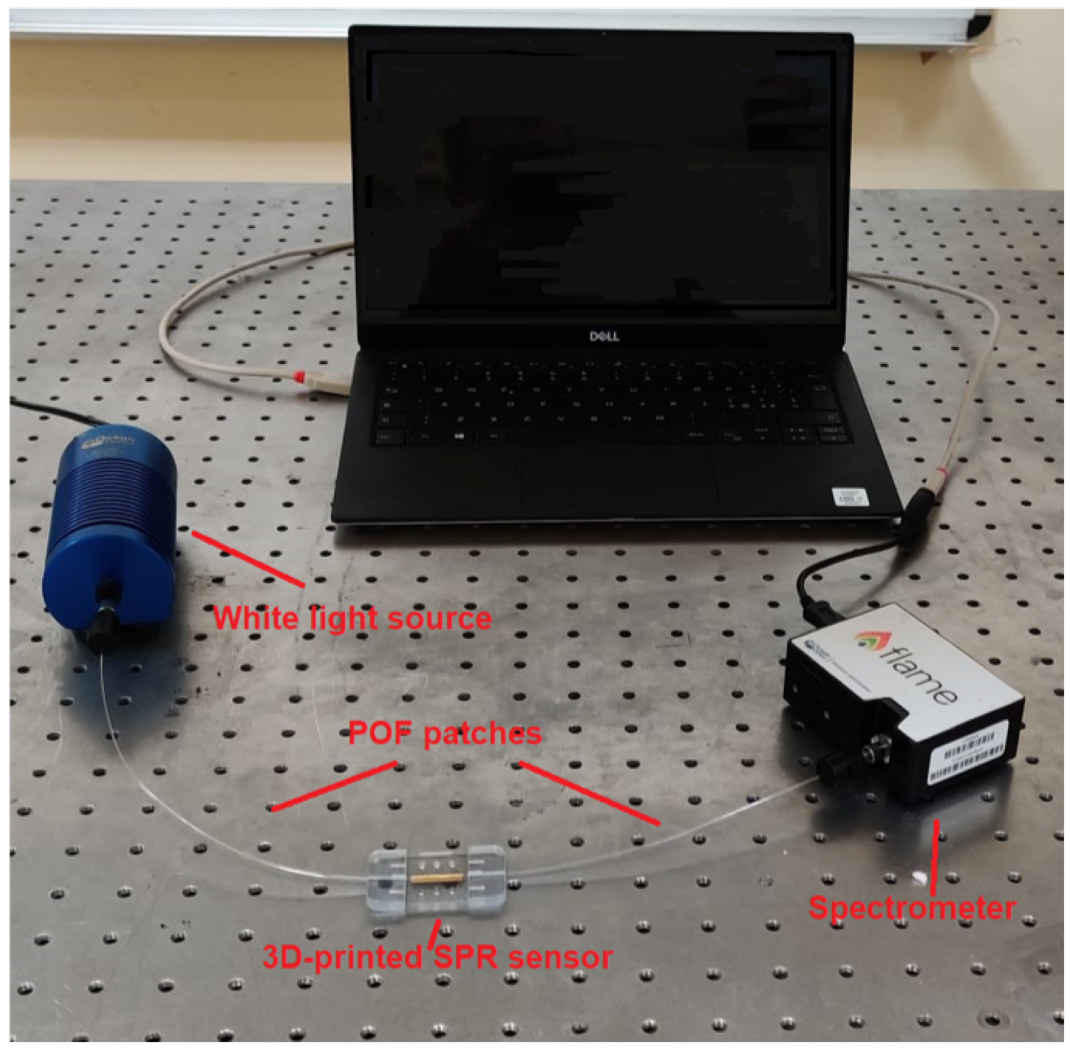
2.2. Testing Experimental Setup
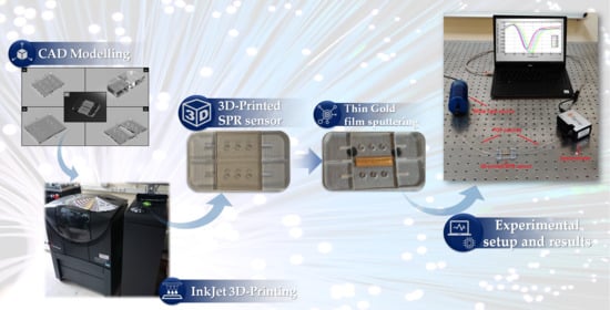
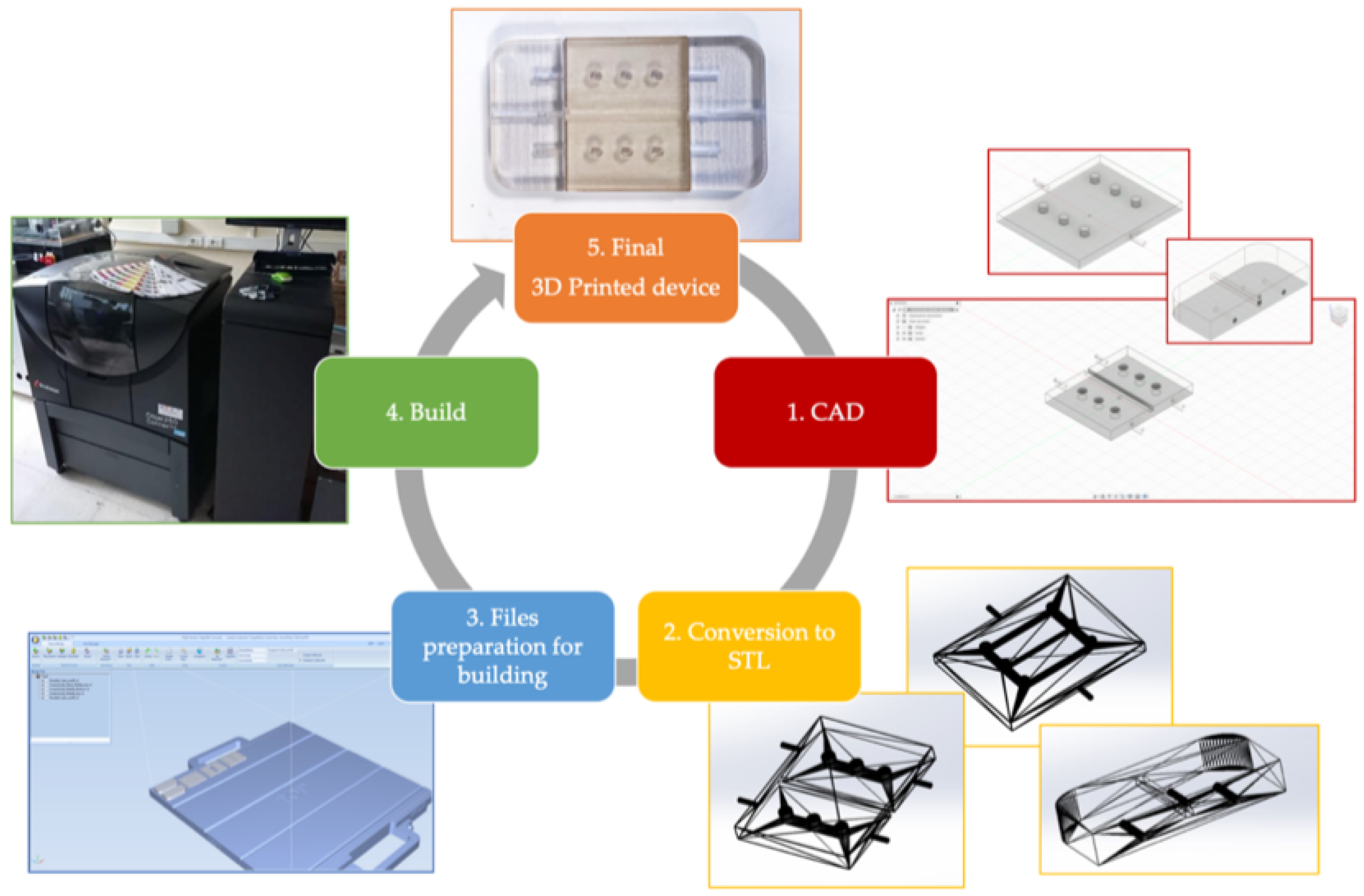
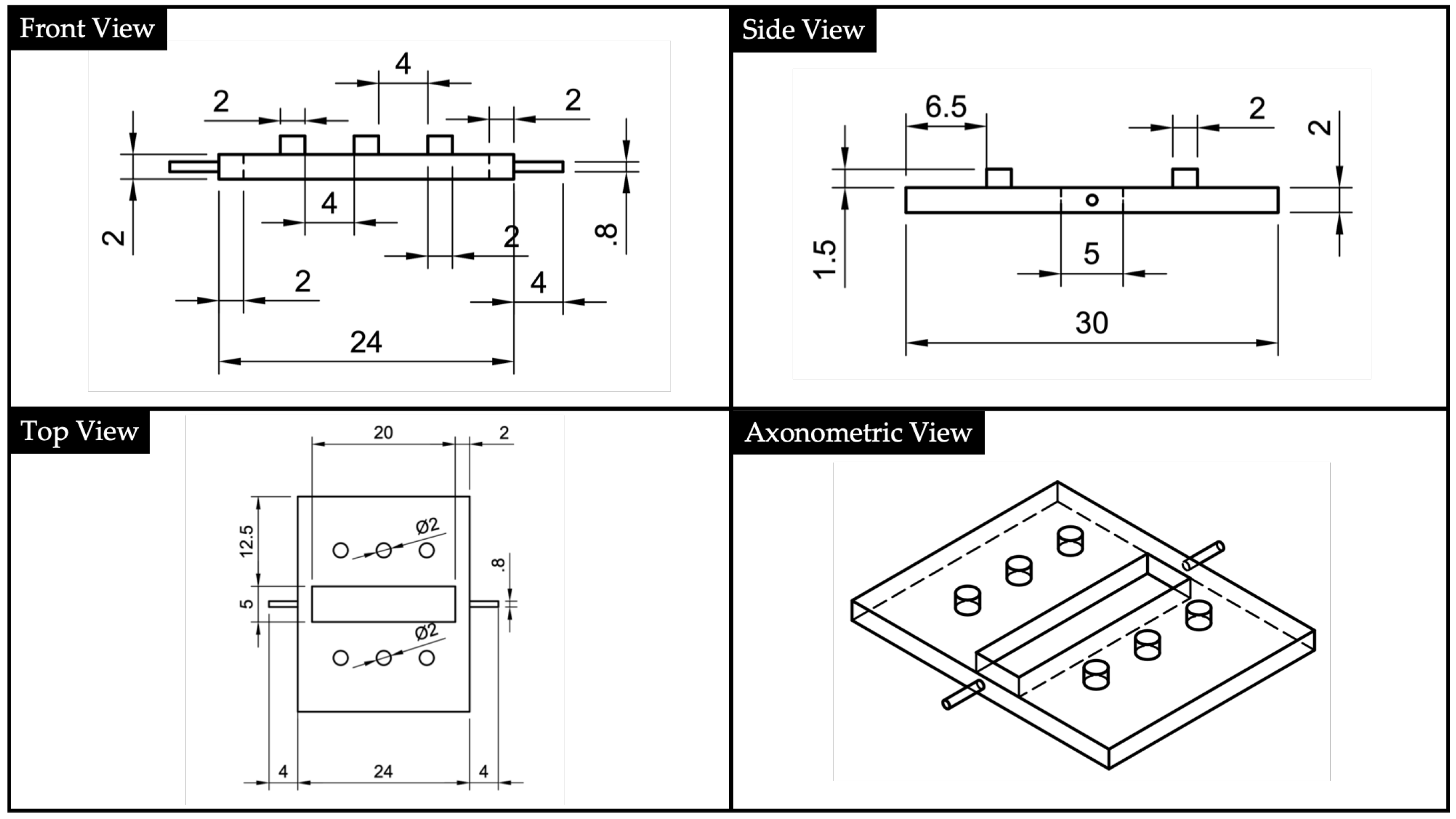
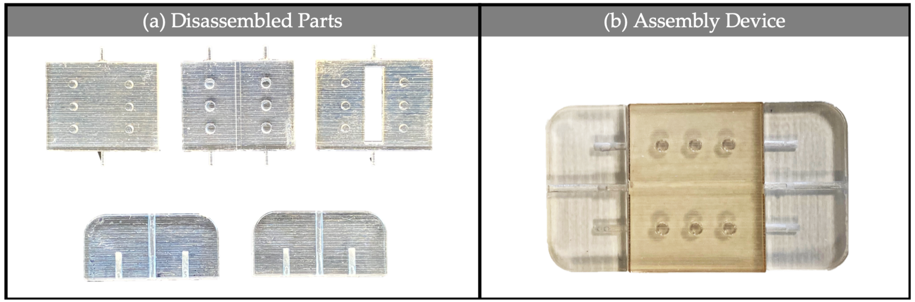
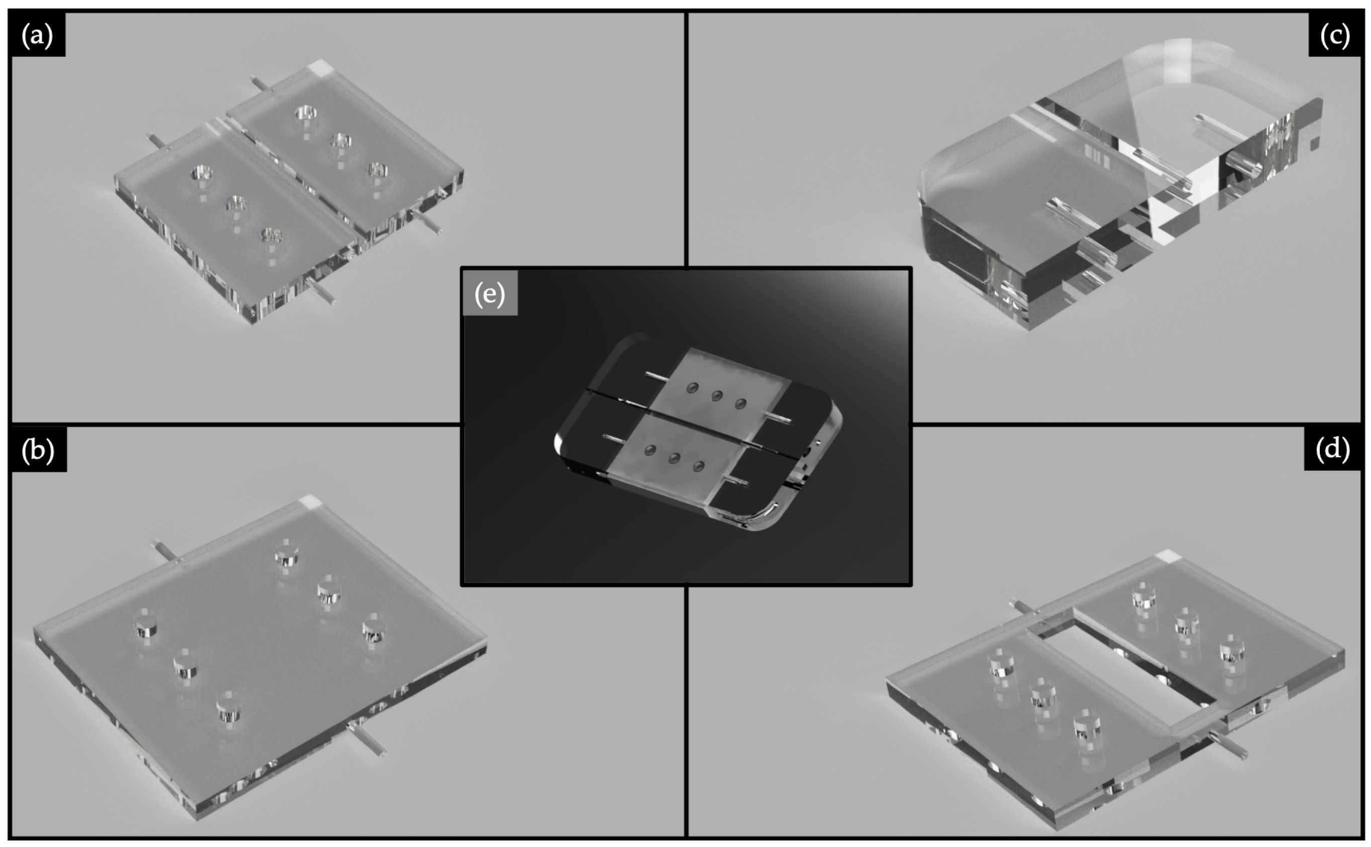
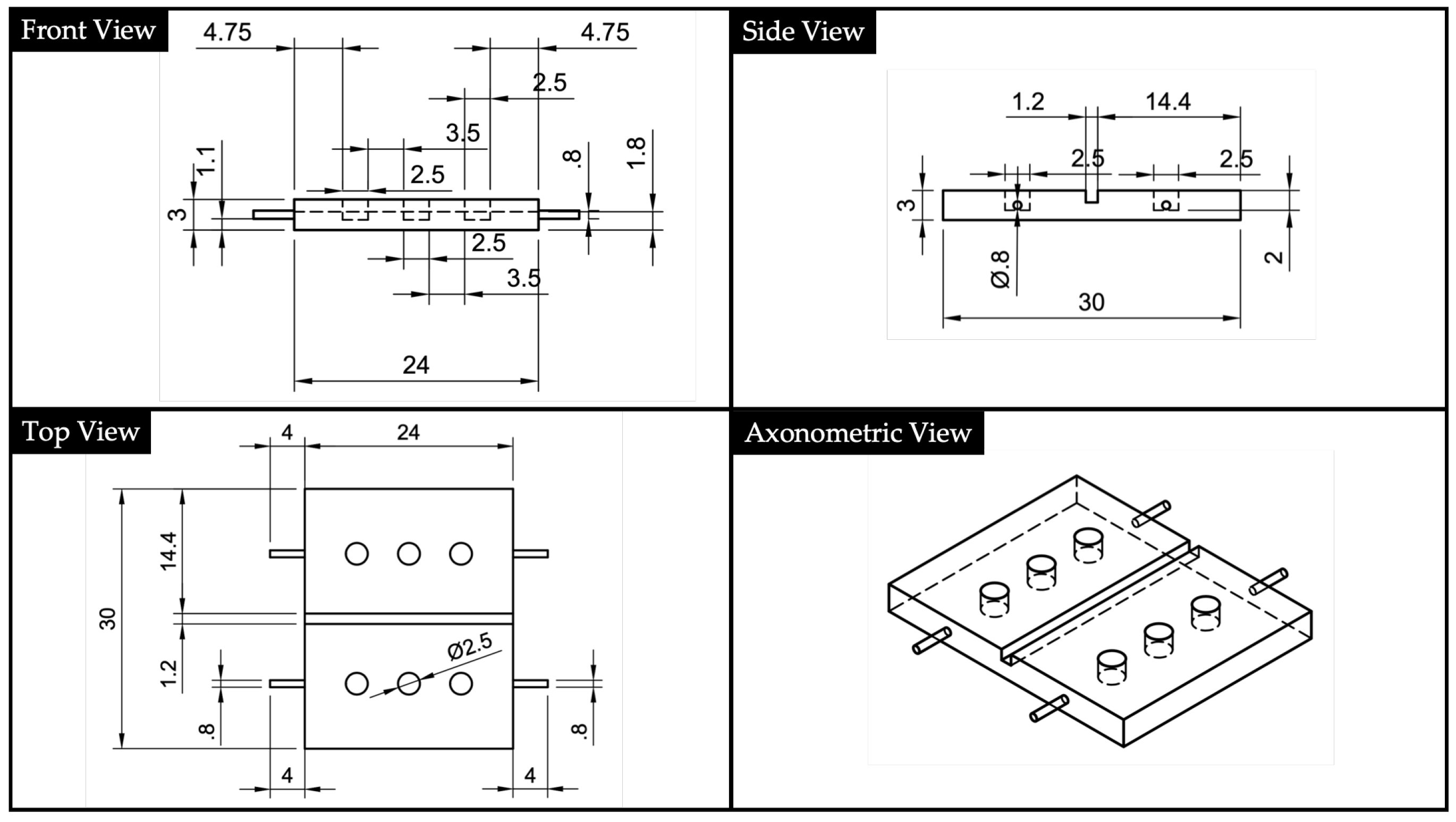
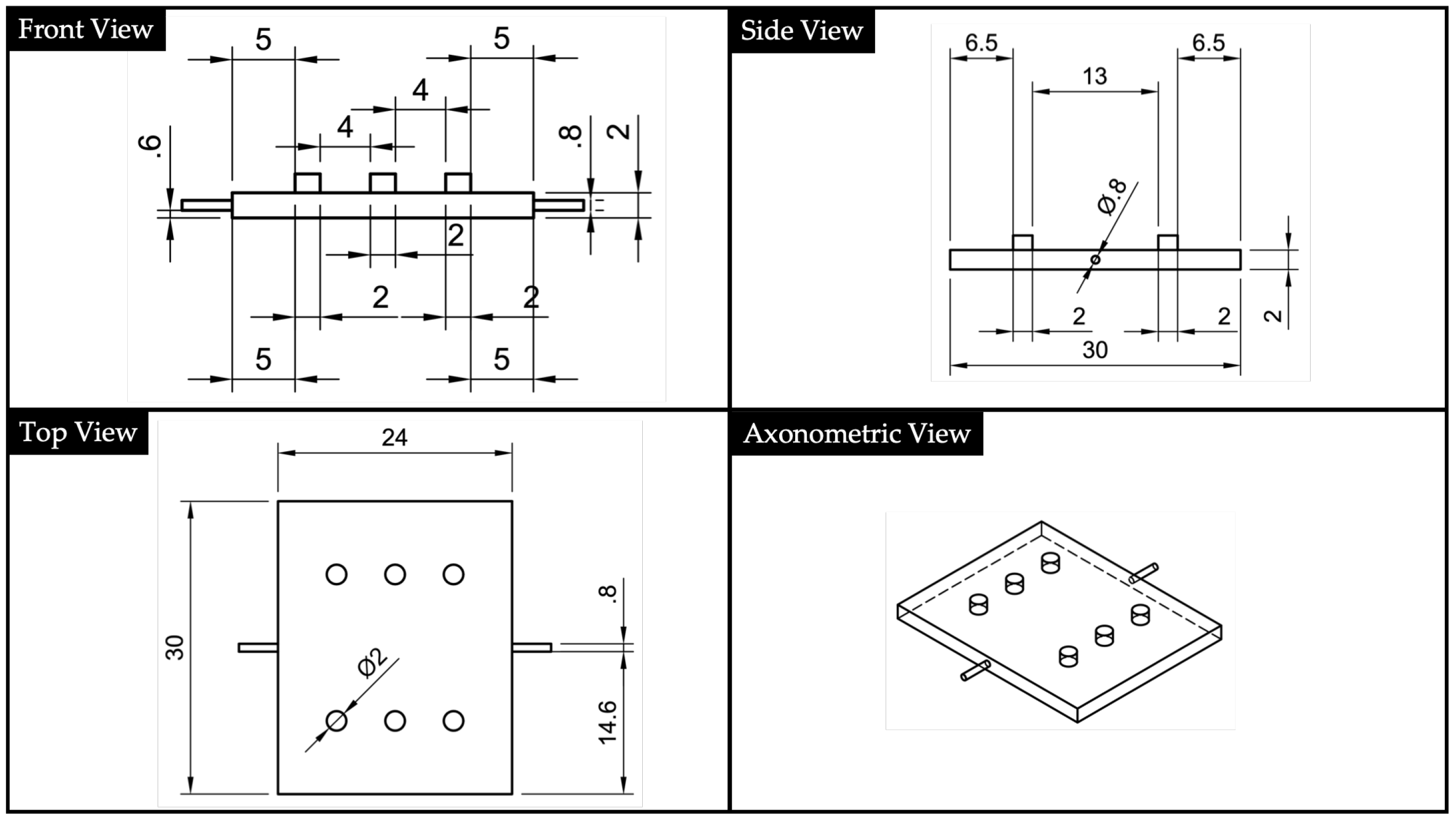
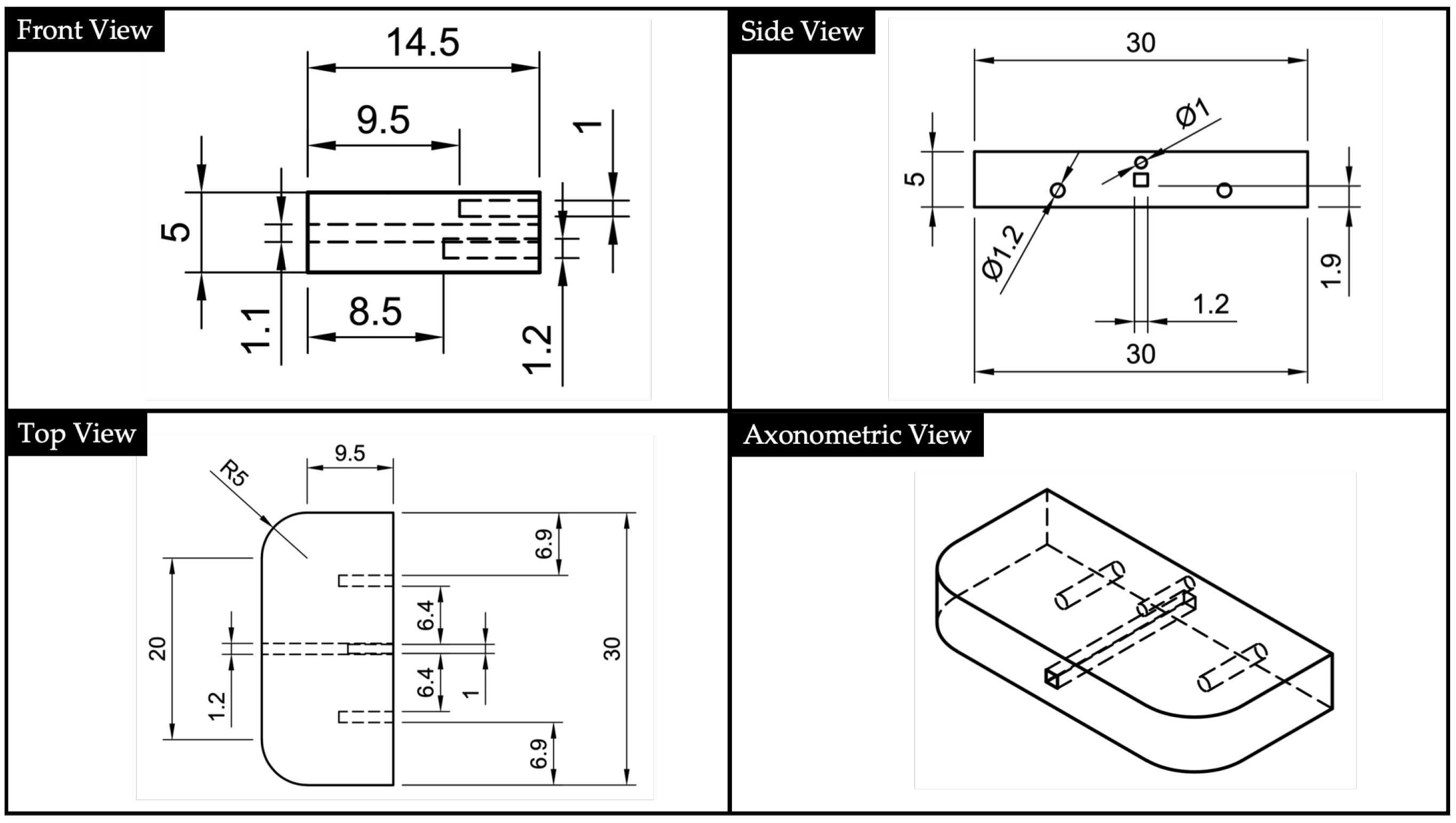
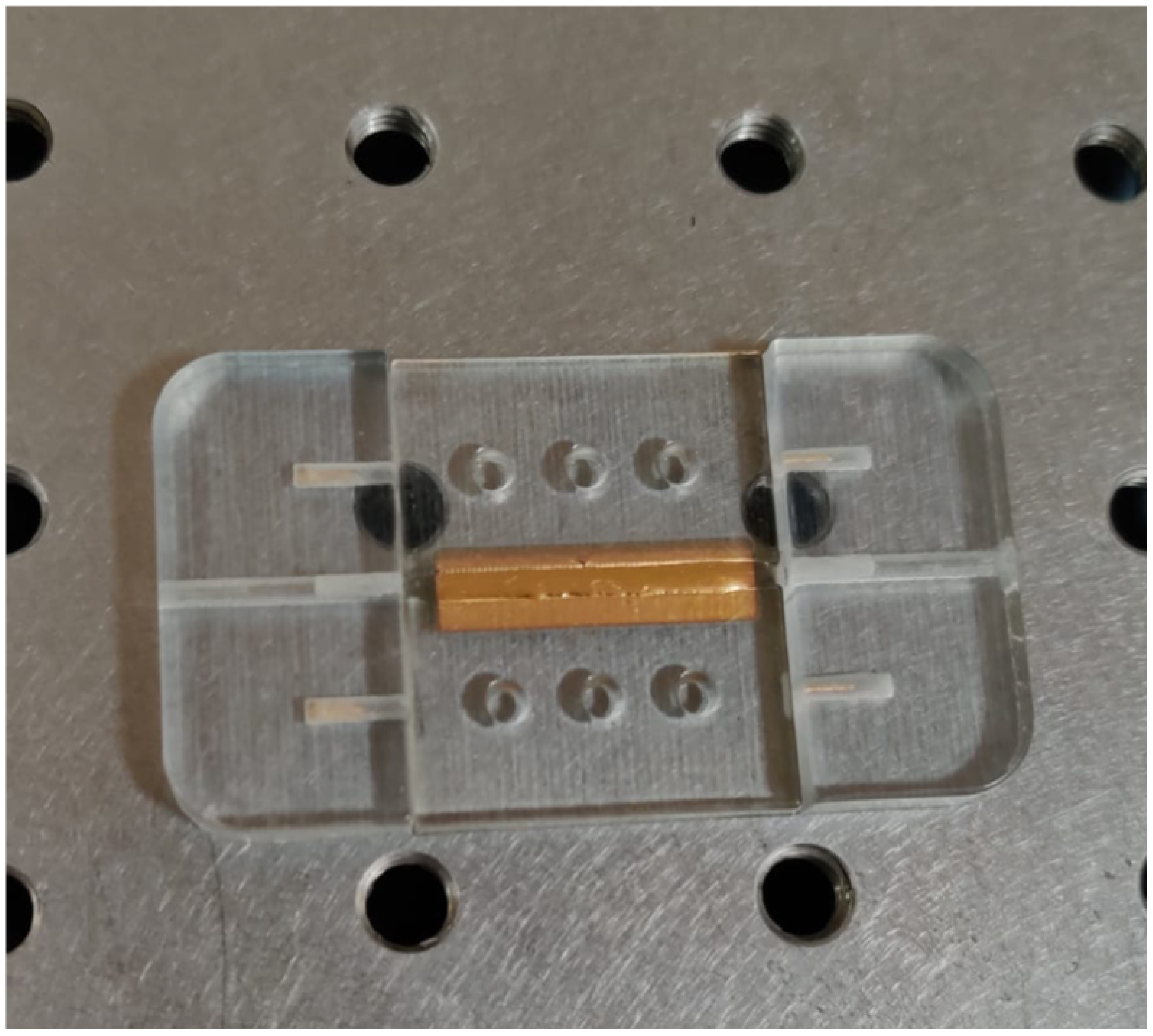
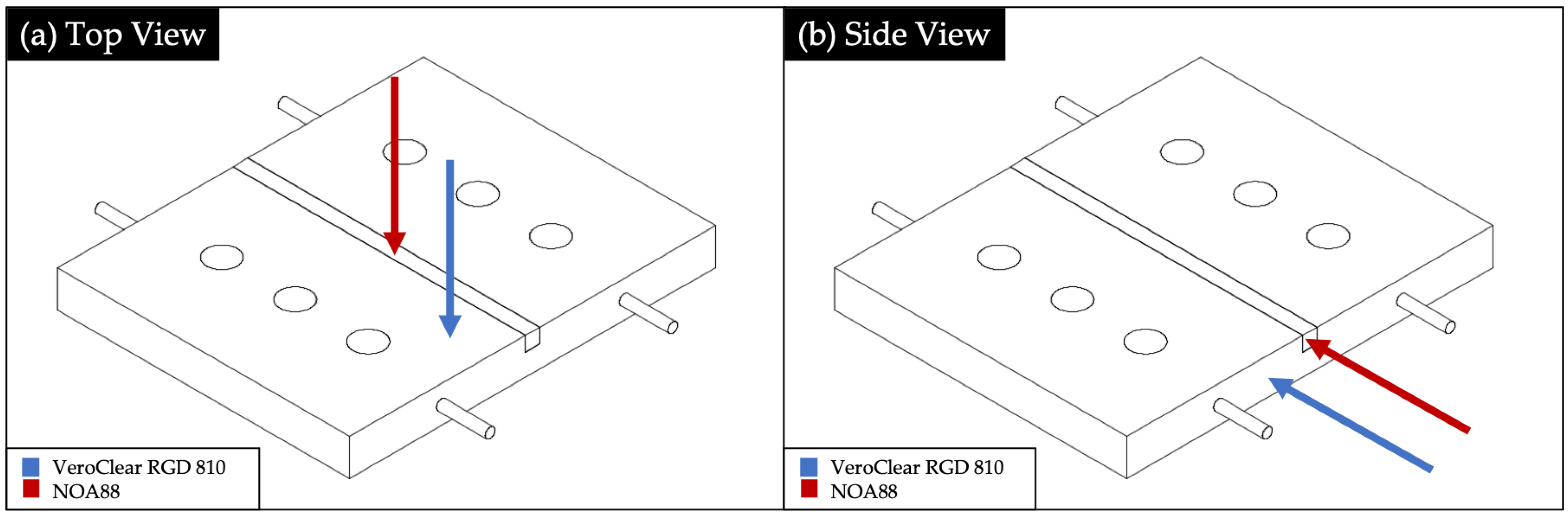
2.3. Device Design and Process of Fabrication
3. Results
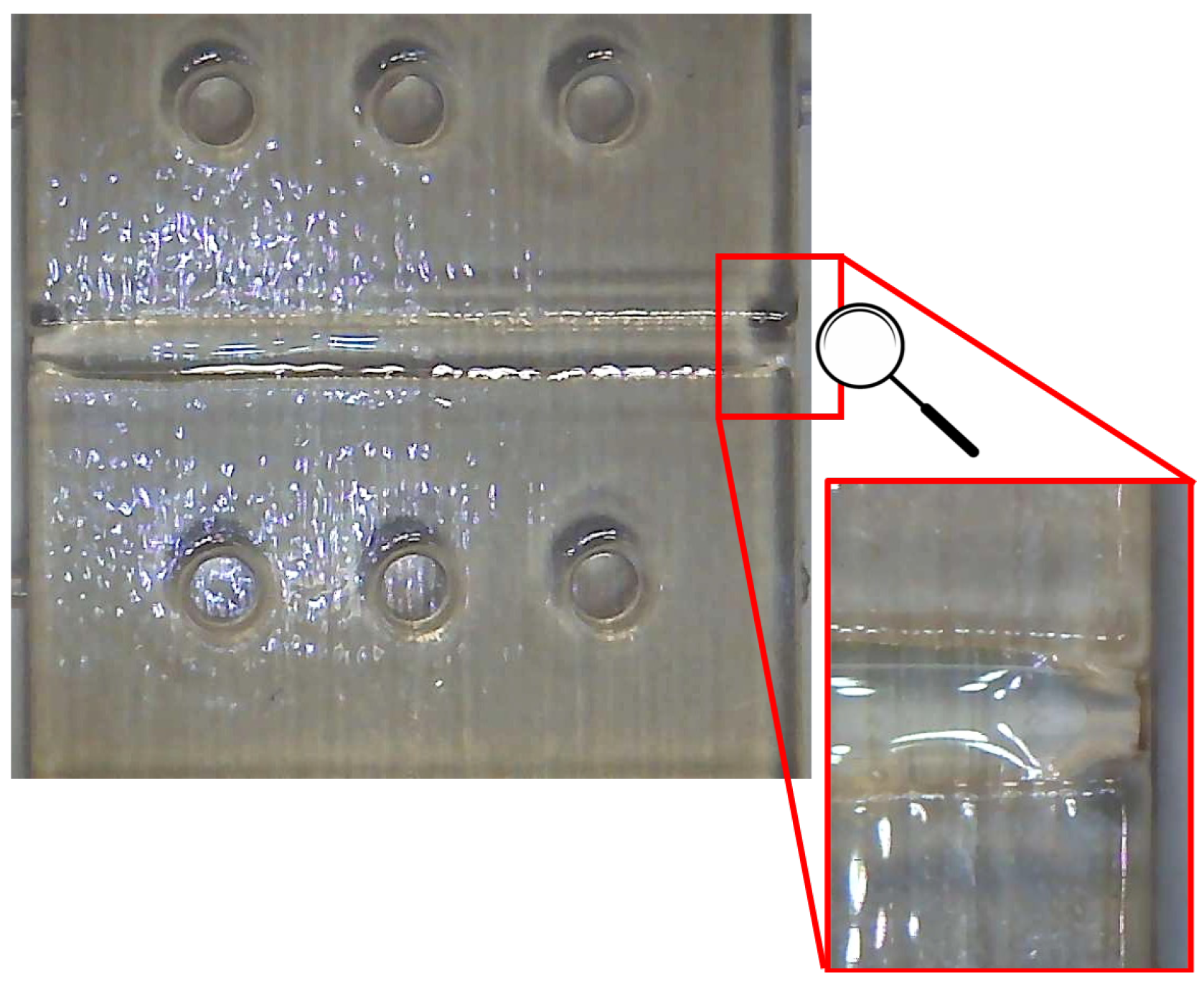
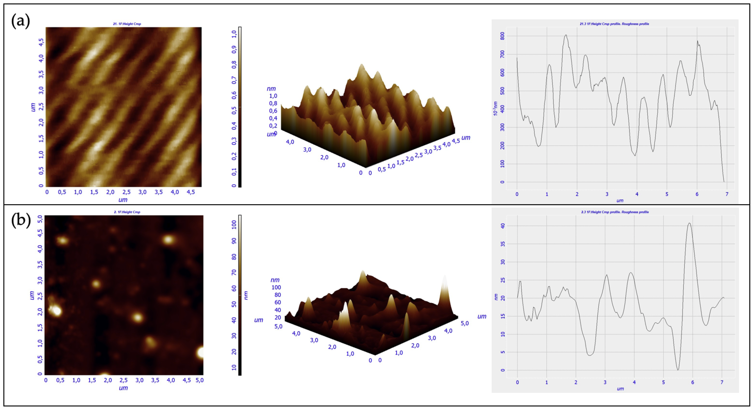
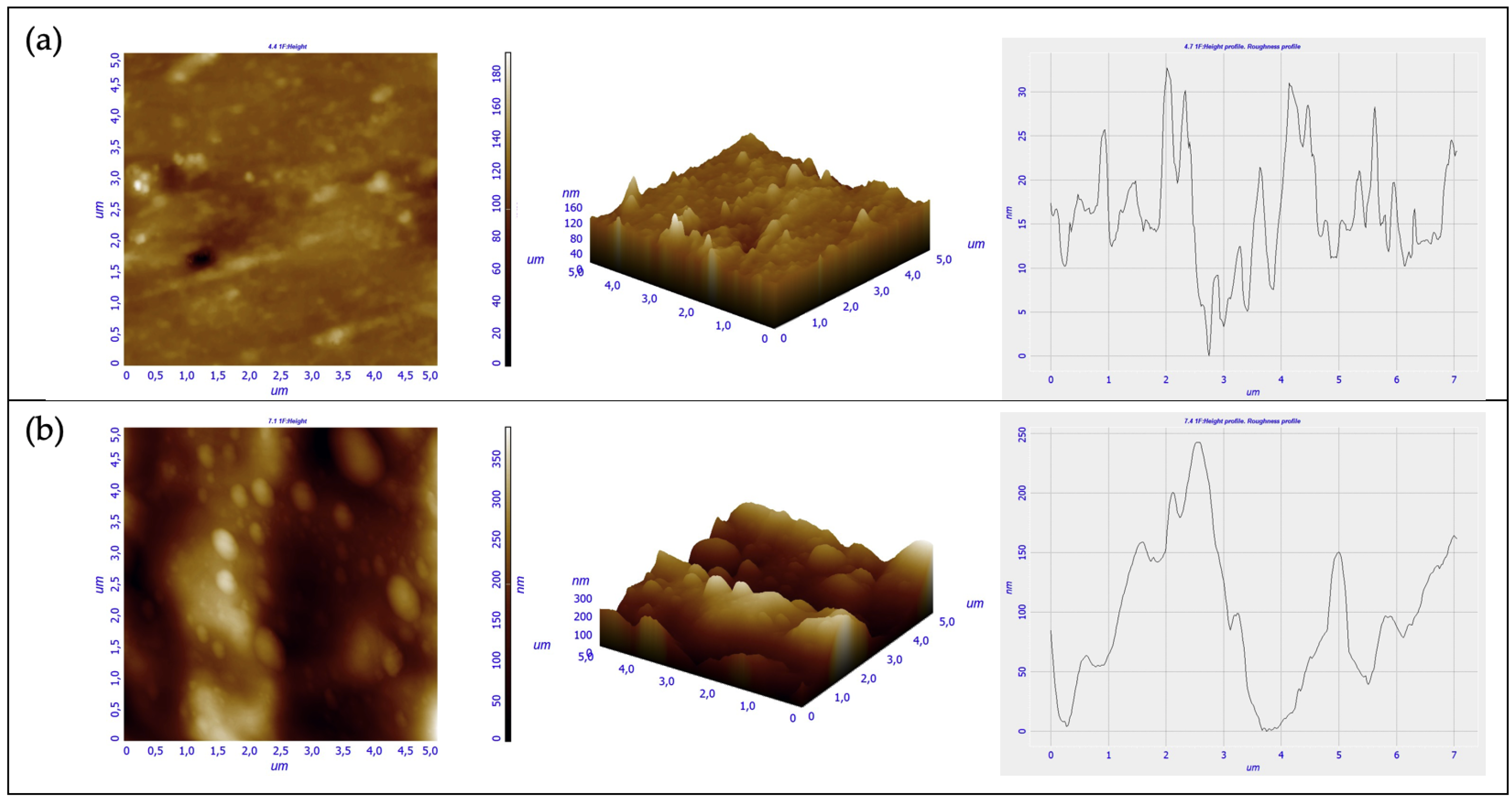
3.1. AFM Analysis
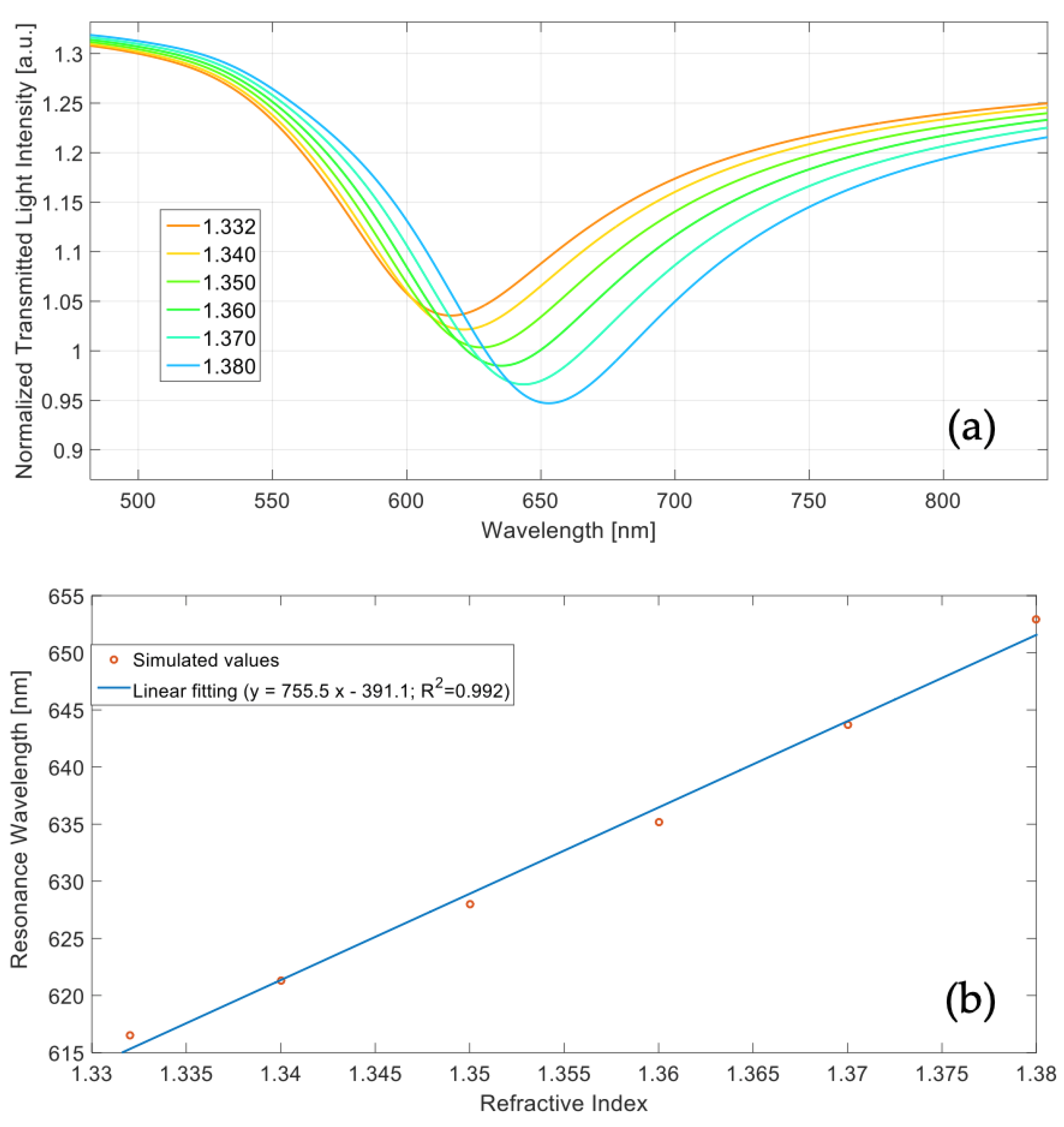
3.2. Numerical Results
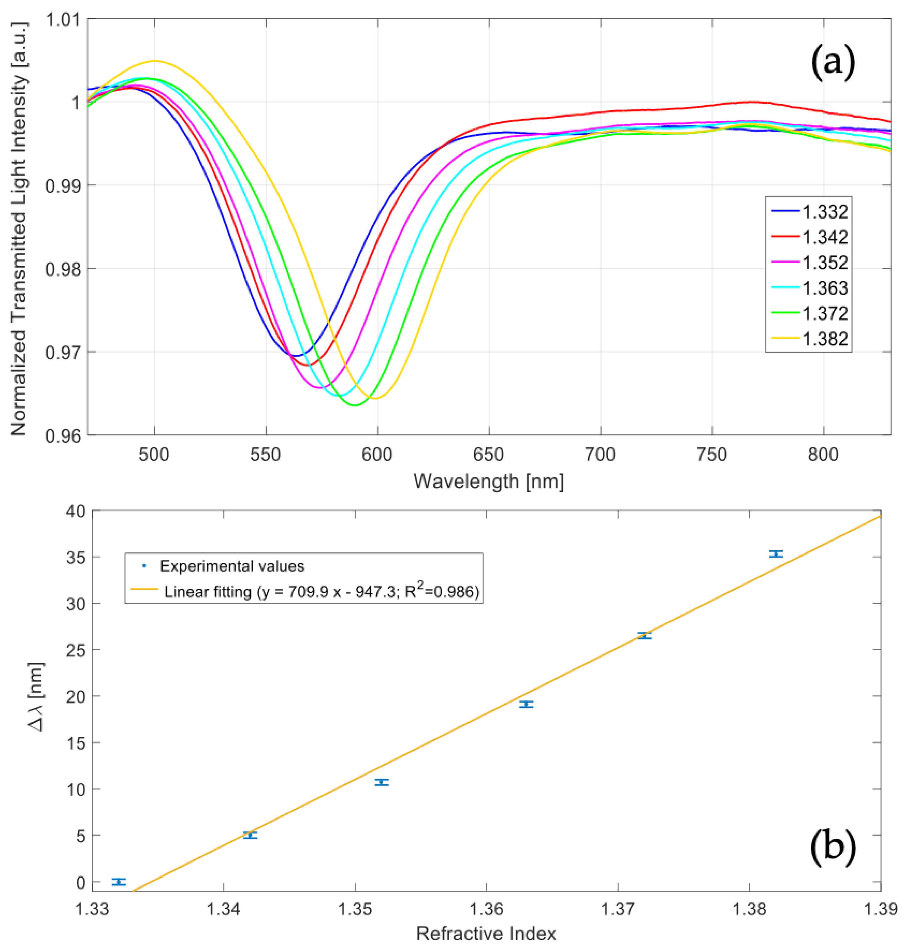
3.3. Experimental Results
4. Discussion
Cost Modelling
- Material costs;
- Machine costs;
- Process costs.
5. Conclusions
Supplementary Materials
Author Contributions
Funding
Institutional Review Board Statement
Informed Consent Statement
Data Availability Statement
Conflicts of Interest
References
- Forrest, S. The path to ubiquitous and low-cost organic electronic appliances on plastic. Nature 2004, 428, 911–918. [Google Scholar] [CrossRef] [PubMed]
- Mitsuhiro, K. OLED Displays and Lighting; Wiley: Hoboken, NJ, USA, 2017. [Google Scholar]
- Di, C.A.; Zhangand, F.; Zhu, D. Multi-Functional Integration of Organic Field-Effect Transistors (OFETs): Advances and Perspectives. Adv. Mater 2013, 25, 313–330. [Google Scholar] [CrossRef] [PubMed]
- Someya, T.; Sakurai, T.; Sekitani, T. Flexible, Large-area sensors and actuators with organic transistor integrated circuits. In Proceedings of the IEEE InternationalElectron Devices Meeting, Washington, DC, USA, 5 December 2005; pp. 44–45. [Google Scholar]
- Changyeon, L.; Seungjin, L.; Geon-U, K.; Wonho, L.; Bumjoon, J.K. Recent Advances, Design Guidelines, and Prospects of All-Polymer Solar Cells. Chem. Rev. 2019, 119, 8028–8086. [Google Scholar]
- Cennamo, N.; Pesavento, M.; Zeni, L. A review on simple and highly sensitive plastic optical fiber probes for bio-chemical sensing. Sens. Actuat. B Chem. 2021, 331, 129393. [Google Scholar] [CrossRef]
- Liu, Y.; Peng, W. Fiber-Optic Surface Plasmon Resonance Sensors and Biochemical Applications: A Review. J. Light. Technol. 2021, 39, 3781–3791. [Google Scholar] [CrossRef]
- Caucheteur, C.; Guo, T.; Albert, J. Review of plasmonic fiber optic biochemical sensors: Improving the limit of detection. Anal. Bioanal. Chem. 2015, 407, 3883–3897. [Google Scholar] [CrossRef] [PubMed]
- Allsop, T.; Neal, R. A Review: Evolution and Diversity of Optical Fibre Plasmonic Sensors. Sensors 2019, 19, 4874. [Google Scholar] [CrossRef] [PubMed] [Green Version]
- Lambert, A.; Valiulis, S.; Cheng, Q. Advances in Optical Sensing and Bioanalysis Enabled by 3D Printing. ACS Sens. 2018, 3, 2475–2491. [Google Scholar] [CrossRef] [PubMed]
- Hinman, S.S.; McKeating, K.S.; Cheng, Q. Plasmonic Sensing with 3D Printed Optics. Anal. Chem. 2017, 89, 12626–12630. [Google Scholar] [CrossRef] [PubMed] [Green Version]
- Haring, A.P.; Khan, A.U.; Liu, G.; Johnson, B.N. 3D Printed Functionally Graded Plasmonic Constructs. Adv. Optical Mater. 2017, 5, 1700367. [Google Scholar] [CrossRef]
- Garciá-Astrain, C.; Lenzi, E.; de Aberasturi, D.J.; Henriksen-Lacey, M.; Binelli, M.R.; Liz-Marzaán, L.M. 3D-Printed Biocompatible Scaffolds with Built-In Nanoplasmonic Sensors. Adv. Funct. Mater. 2020, 30, 2005407. [Google Scholar] [CrossRef]
- Cairone, F.; Gagliano, S.; Carbone, D.C.; Recca, G.; Bucolo, M. Micro-optofluidic switch realized by 3D printing technology. Microfluid. Nanofluidics 2016, 20, 61. [Google Scholar] [CrossRef]
- Cairone, F.; Anandan, P.; Bucolo, M. Nonlinear systems synchronization for modeling two-phase microfluidics flows. Nonlinear Dyn. 2018, 92, 75–84. [Google Scholar] [CrossRef]
- Anandan, P.; Gagliano, S.; Bucolo, M. Computational models in microfluidic bubble logic. Microfluid. Nanofluidics 2014, 18, 305–321. [Google Scholar] [CrossRef]
- Xu, Y.; Wu, X.; Guo, X.; Kong, B.; Zhang, M.; Qian, X.; Mi, S.; Sun, W. The Boom in 3D-Printed Sensor Technology. Sensors 2017, 17, 1166. [Google Scholar] [CrossRef] [PubMed]
- Prajzler, V.; Kulha, P.; Knietel, M.; Enser, H. Large core plastic planar optical splitter fabricated by 3D printing technology. Opt. Commun. 2017, 400, 38–42. [Google Scholar] [CrossRef]
- Rezem, M.; Gunther, A.; Roth, B.; Reithmeier, E.; Rahlves, M. Low-Cost Fabrication of All-Polymer Components for Integrated Photonics. J. Light. Technol. 2017, 35, 299–308. [Google Scholar] [CrossRef]
- Alford, T.L.; Feldman, L.C.; Mayer, J.W. Fundamentals of Nanoscale Film Analysis; Springer: Berlin/Heidelberg, Germany, 2007. [Google Scholar]
- Kanso, M.; Cuenot, S.; Louarn, G. Sensitivity of Optical Fiber Sensor Based on Surface Plasmon Resonance: Modeling and Experiments. Plasmonics 2008, 3, 49–57. [Google Scholar] [CrossRef]
- Cennamo, N.; Massarotti, D.; Conte, L.; Zeni, L. Low Cost Sensors Based on SPR in a Plastic Optical Fiber for Biosensor Implementation. Sensors 2011, 11, 11752–11760. [Google Scholar] [CrossRef] [PubMed]
- Cennamo, N.; Coelho, L.; Santos, D.F.; Baptista, J.M.; Guerreiro, A.; Jorge, P.A.S.; Zeni, L. Modal Filtering for Optimized Surface Plasmon Resonance Sensing in Multimode Plastic Optical Fibers. IEEE Sens. J. 2015, 15, 6306–6312. [Google Scholar] [CrossRef]


| View Investigate | Material Investigated | RMS [nm] | RA [nm] | Peak to Peak [nm] |
|---|---|---|---|---|
| Top View | VeroClear RGD810 | 0.163 | 0.131 | 1.094 |
| Side View | VeroClear RGD810 | 10.508 | 6.858 | 192.907 |
| Top View | NOA88 | 12.333 | 7.182 | 140.123 |
| Side View | NOA88 | 70.862 | 59.851 | 388.762 |
| Sensor | Refractive Index | SNR | Sensitivity () [nm/RIU] | FWHM [nm] | FOM [RIU−1] | Reference |
|---|---|---|---|---|---|---|
| SPR-POF | 1.352 | 0.982 | 2.4 · 10 3 | 181 | 13.4 | [22] |
| 3D-printed SPR | 1.352 | 1.387 | 710 | 52 | 13.6 | This work |
| INPUT PARAMETERS | Unit | Value | |
|---|---|---|---|
| Material | VeroClear RGD810 | €/kg | 393.11 |
| FullCure705 | €/kg | 126.74 | |
| Norland Optical Adhesive NOA 88 | €/mL | 2.50 | |
| Part | Model | kg | 0.017 |
| Support | kg | 0.006 | |
| Printing Time | h | 0.47 | |
| Optical Adhesive | mL | 1.00 | |
| Machine | Depreciation Cost | €/kg | 10.00 |
| Process | Power Cost | €/kWh | 0.10 |
| Labour | €/h | 0 |
| Total Cost for one Assembly Device | % | € |
|---|---|---|
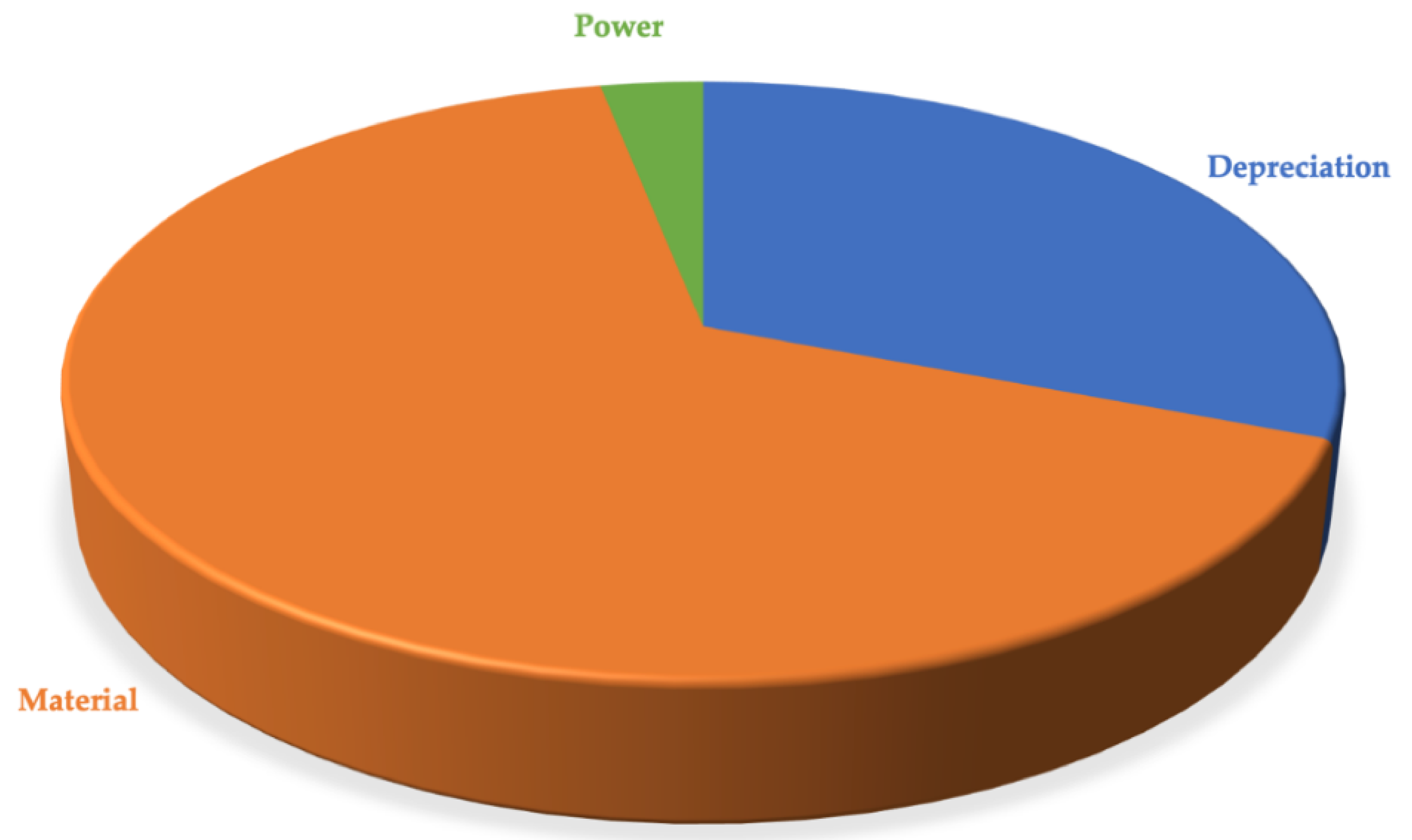
| Depreciation | 31% | 4.67 |
| Material | 66% | 9.94 |
| Power | 3% | 0.47 |
| Total Cost | 15.08 |
Publisher’s Note: MDPI stays neutral with regard to jurisdictional claims in published maps and institutional affiliations. |
© 2021 by the authors. Licensee MDPI, Basel, Switzerland. This article is an open access article distributed under the terms and conditions of the Creative Commons Attribution (CC BY) license (https://creativecommons.org/licenses/by/4.0/).
Share and Cite
Cennamo, N.; Saitta, L.; Tosto, C.; Arcadio, F.; Zeni, L.; Fragalá, M.E.; Cicala, G. Microstructured Surface Plasmon Resonance Sensor Based on Inkjet 3D Printing Using Photocurable Resins with Tailored Refractive Index. Polymers 2021, 13, 2518. https://doi.org/10.3390/polym13152518
Cennamo N, Saitta L, Tosto C, Arcadio F, Zeni L, Fragalá ME, Cicala G. Microstructured Surface Plasmon Resonance Sensor Based on Inkjet 3D Printing Using Photocurable Resins with Tailored Refractive Index. Polymers. 2021; 13(15):2518. https://doi.org/10.3390/polym13152518
Chicago/Turabian StyleCennamo, Nunzio, Lorena Saitta, Claudio Tosto, Francesco Arcadio, Luigi Zeni, Maria Elena Fragalá, and Gianluca Cicala. 2021. "Microstructured Surface Plasmon Resonance Sensor Based on Inkjet 3D Printing Using Photocurable Resins with Tailored Refractive Index" Polymers 13, no. 15: 2518. https://doi.org/10.3390/polym13152518
APA StyleCennamo, N., Saitta, L., Tosto, C., Arcadio, F., Zeni, L., Fragalá, M. E., & Cicala, G. (2021). Microstructured Surface Plasmon Resonance Sensor Based on Inkjet 3D Printing Using Photocurable Resins with Tailored Refractive Index. Polymers, 13(15), 2518. https://doi.org/10.3390/polym13152518