Recent Progress in Carbon-Based Buffer Layers for Polymer Solar Cells


 ,
,  , ,
, ,  and
and 
Abstract
:
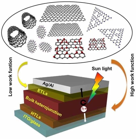
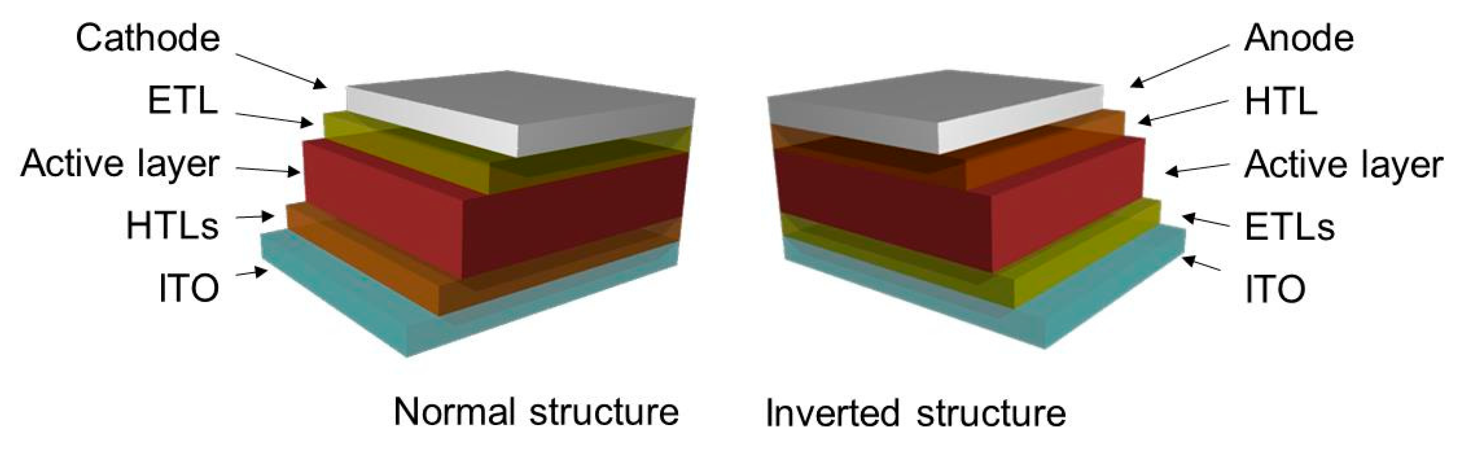
1. Introduction
2. Structures and Properties
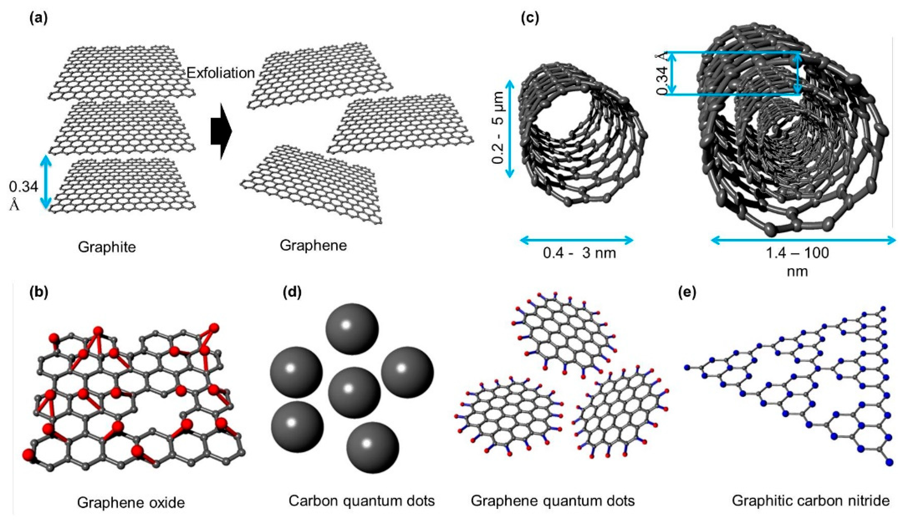
2.1. Graphene
2.2. Graphene Oxide
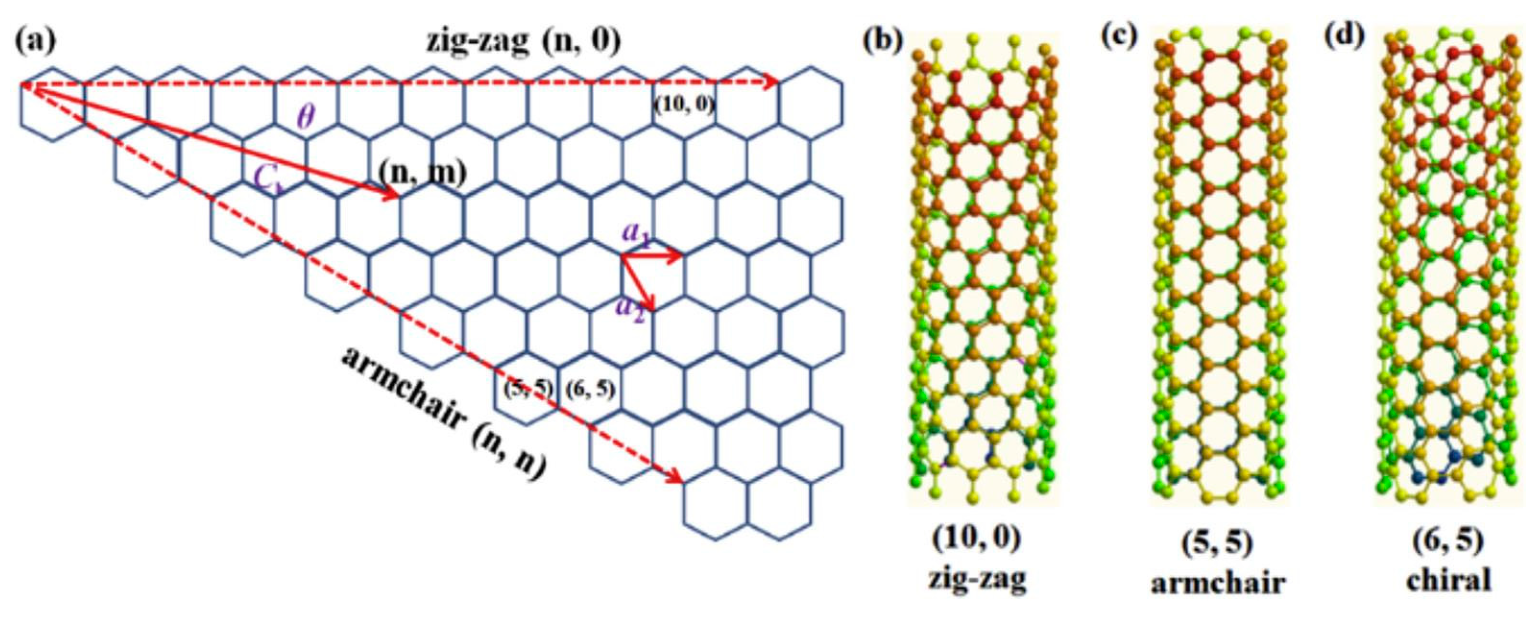
2.3. Carbon Nanotube
2.4. Carbon and Graphene Quantum Dots
2.5. Graphitic Carbon Nitride
3. Application of Carbon Buffer Layers in PSCs
3.1. Graphene Buffer Layers
3.2. Graphene Oxide Buffer Layers
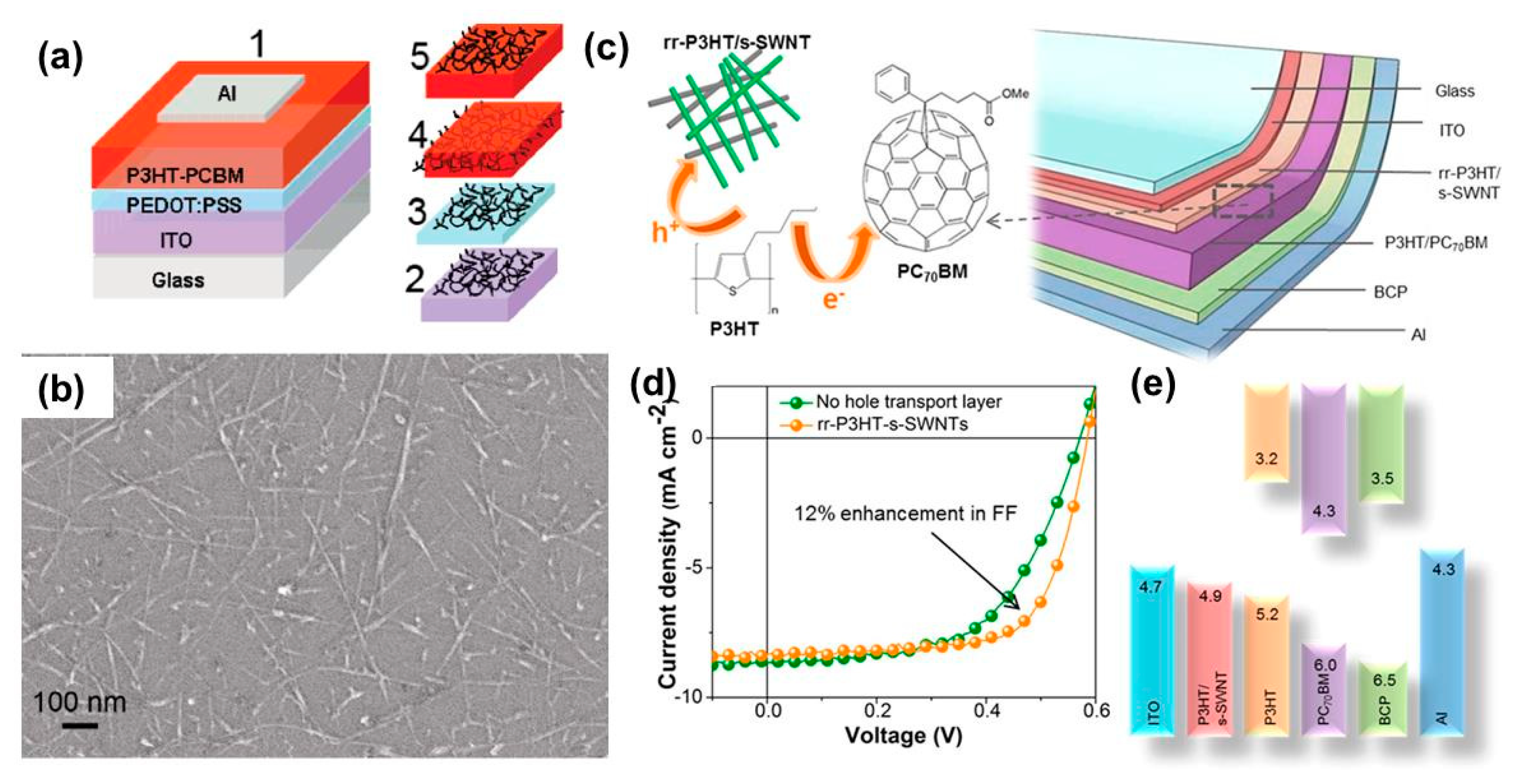
3.3. Carbon Nanotube Buffer Layers
3.4. Graphene Quantum Dots Buffer Layers
3.5. Graphitic Carbon Nitrides
4. Conclusions and Outlooks
Author Contributions
Funding
Conflicts of Interest
References
- Blakers, A.; Zin, N.; McIntosh, K.R.; Fong, K. High Efficiency Silicon Solar Cells. Energy Procedia 2013, 33, 1–10. [Google Scholar] [CrossRef]
- Kumar, A.; Bieri, M.; Reindl, T.; Aberle, A.G. Economic Viability Analysis of Silicon Solar Cell Manufacturing: Al-BSF versus PERC. Energy Procedia 2017, 130, 43–49. [Google Scholar] [CrossRef]
- Pan, Z.; Rao, H.; Mora-Seró, I.; Bisquert, J.; Zhong, X. Quantum dot-sensitized solar cells. Chem. Soc. Rev. 2018, 47, 7659–7702. [Google Scholar] [CrossRef] [PubMed]
- Ganesan, A.A.; Houtepen, A.J.; Crisp, R.W. Quantum Dot Solar Cells: Small Beginnings Have Large Impacts. Appl. Sci. 2018, 8, 1867. [Google Scholar] [CrossRef]
- Ahmad, W.; He, J.; Liu, Z.; Xu, K.; Chen, Z.; Yang, X.; Li, D.; Xia, Y.; Zhang, J.; Chen, C. Lead Selenide (PbSe) Colloidal Quantum Dot Solar Cells with >10% Efficiency. Adv. Mater. 2019, 31, 1900593. [Google Scholar] [CrossRef] [PubMed]
- Gong, J.; Sumathy, K.; Qiao, Q.; Zhou, Z. Review on dye-sensitized solar cells (DSSCs): Advanced techniques and research trends. Renew. Sustain. Energ. Rev. 2017, 68, 234–246. [Google Scholar] [CrossRef]
- Upadhyaya, H.M.; Senthilarasu, S.; Hsu, M.-H.; Kumar, D.K. Recent progress and the status of dye-sensitised solar cell (DSSC) technology with state-of-the-art conversion efficiencies. Sol. Energy Mater. Sol. Cells 2013, 119, 291–295. [Google Scholar] [CrossRef]
- Hou, W.; Xiao, Y.; Han, G.; Lin, J.-Y. The Applications of Polymers in Solar Cells: A Review. Polymers 2019, 11, 143. [Google Scholar] [CrossRef]
- Sun, H.; Chen, F.; Chen, Z.-K. Recent progress on non-fullerene acceptors for organic photovoltaics. Mater. Today 2019, 24, 94–118. [Google Scholar] [CrossRef]
- Wang, G.; Melkonyan, F.S.; Facchetti, A.; Marks, T.J. All-Polymer Solar Cells: Recent Progress, Challenges, and Prospects. Angew. Chem. Int. Ed. 2019, 58, 4129–4142. [Google Scholar] [CrossRef]
- Liu, Z.; Zhang, L.; Shao, M.; Wu, Y.; Zeng, D.; Cai, X.; Duan, J.; Zhang, X.; Gao, X. Fine-Tuning the Quasi-3D Geometry: Enabling Efficient Nonfullerene Organic Solar Cells Based on Perylene Diimides. ACS Appl. Mater. Interfaces 2018, 10, 762–768. [Google Scholar] [CrossRef] [PubMed]
- Liu, Z.; Wu, Y.; Zhang, Q.; Gao, X. Non-fullerene small molecule acceptors based on perylene diimides. J. Mater. Chem. A 2016, 4, 17604–17622. [Google Scholar] [CrossRef]
- Ramanujam, J.; Singh, U.P. Copper indium gallium selenide based solar cells—A review. Energy Environ. Sci. 2017, 10, 1306–1319. [Google Scholar] [CrossRef]
- Tai, Q.; Tang, K.-C.; Yan, F. Recent progress of inorganic perovskite solar cells. Energy Environ. Sci. 2019, 12, 2375–2405. [Google Scholar] [CrossRef]
- Assadi, M.K.; Bakhoda, S.; Saidur, R.; Hanaei, H. Recent progress in perovskite solar cells. Renew. Sustain. Energ. Rev. 2018, 81, 2812–2822. [Google Scholar] [CrossRef]
- Shi, Z.; Jayatissa, A.H. Perovskites-Based Solar Cells: A Review of Recent Progress, Materials and Processing Methods. Materials 2018, 11, 729. [Google Scholar] [CrossRef]
- Espinosa, N.; Dam, H.F.; Tanenbaum, D.M.; Andreasen, J.W.; Jørgensen, M.; Krebs, F.C. Roll-to-Roll Processing of Inverted Polymer Solar Cells using Hydrated Vanadium(V)Oxide as a PEDOT:PSS Replacement. Materials 2011, 4, 169–182. [Google Scholar] [CrossRef]
- Gu, X.; Zhou, Y.; Gu, K.; Kurosawa, T.; Guo, Y.; Li, Y.; Lin, H.; Schroeder, B.C.; Yan, H.; Molina-Lopez, F.; et al. Roll-to-Roll Printed Large-Area All-Polymer Solar Cells with 5% Efficiency Based on a Low Crystallinity Conjugated Polymer Blend. Adv. Energy Mater. 2017, 7, 1602742. [Google Scholar] [CrossRef]
- Sun, C.; Pan, F.; Bin, H.; Zhang, J.; Xue, L.; Qiu, B.; Wei, Z.; Zhang, Z.-G.; Li, Y. A low cost and high performance polymer donor material for polymer solar cells. Nat. Commun. 2018, 9, 743. [Google Scholar] [CrossRef]
- Lu, S.; Sun, Y.; Ren, K.; Liu, K.; Wang, Z.; Qu, S. Recent Development in ITO-free Flexible Polymer Solar Cells. Polymers 2018, 10, 5. [Google Scholar] [CrossRef]
- Cheng, P.; Zhan, X. Stability of organic solar cells: Challenges and strategies. Chem. Soc. Rev. 2016, 45, 2544–2582. [Google Scholar] [CrossRef] [PubMed]
- Mirsafaei, M.; Fallahpour, A.H.; Lugli, P.; Rubahn, H.-G.; Adam, J.; Madsen, M. The influence of electrical effects on device performance of organic solar cells with nano-structured electrodes. Sci. Rep. 2017, 7, 5300. [Google Scholar] [CrossRef] [PubMed]
- Po, R.; Carbonera, C.; Bernardi, A.; Camaioni, N. The role of buffer layers in polymer solar cells. Energy Environ. Sci. 2011, 4, 285–310. [Google Scholar] [CrossRef]
- Kim, Y.-H.; Lee, S.-H.; Noh, J.; Han, S.-H. Performance and stability of electroluminescent device with self-assembled layers of poly(3,4-ethylenedioxythiophene)–poly(styrenesulfonate) and polyelectrolytes. Thin Solid Films 2006, 510, 305–310. [Google Scholar] [CrossRef]
- Jørgensen, M.; Norrman, K.; Krebs, F.C. Stability/degradation of polymer solar cells. Sol. Energy Mater. Sol. Cells 2008, 92, 686–714. [Google Scholar] [CrossRef]
- Kawano, K.; Pacios, R.; Poplavskyy, D.; Nelson, J.; Bradley, D.D.C.; Durrant, J.R. Degradation of organic solar cells due to air exposure. Sol. Energy Mater. Sol. Cells 2006, 90, 3520–3530. [Google Scholar] [CrossRef]
- Dubey, R.; Guruviah, V. Review of carbon-based electrode materials for supercapacitor energy storage. Ionics 2019, 25, 1419–1445. [Google Scholar] [CrossRef]
- Najib, S.; Erdem, E. Current progress achieved in novel materials for supercapacitor electrodes: Mini review. Nanoscale Adv. 2019, 1, 2817–2827. [Google Scholar] [CrossRef]
- Zhang, L.; Wang, Y.; Niu, Z.; Chen, J. Advanced nanostructured carbon-based materials for rechargeable lithium-sulfur batteries. Carbon N. Y. 2019, 141, 400–416. [Google Scholar] [CrossRef]
- Roselin, L.S.; Juang, R.-S.; Hsieh, C.-T.; Sagadevan, S.; Umar, A.; Selvin, R.; Hegazy, H.H. Recent Advances and Perspectives of Carbon-Based Nanostructures as Anode Materials for Li-ion Batteries. Materials 2019, 12, 1229. [Google Scholar] [CrossRef]
- Lam, E.; Luong, J.H.T. Carbon Materials as Catalyst Supports and Catalysts in the Transformation of Biomass to Fuels and Chemicals. ACS Catal. 2014, 4, 3393–3410. [Google Scholar] [CrossRef]
- Anthonysamy, S.B.I.; Afandi, S.B.; Khavarian, M.; Mohamed, A.R.B. A review of carbon-based and non-carbon-based catalyst supports for the selective catalytic reduction of nitric oxide. Beilstein J. Nanotechnol. 2018, 9, 740–761. [Google Scholar] [CrossRef]
- Meng, F.; Liu, A.; Gao, L.; Cao, J.; Yan, Y.; Wang, N.; Fan, M.; Wei, G.; Ma, T. Current progress in interfacial engineering of carbon-based perovskite solar cells. J. Mater. Chem. A 2019, 7, 8690–8699. [Google Scholar] [CrossRef]
- Ferguson, V.; Silva, S.R.P.; Zhang, W. Carbon Materials in Perovskite Solar Cells: Prospects and Future Challenges. Energy Environ. Mater. 2019, 2, 107–118. [Google Scholar] [CrossRef] [Green Version]
- Guo, C.X.; Guai, G.H.; Li, C.M. Graphene Based Materials: Enhancing Solar Energy Harvesting. Adv. Energy Mater. 2011, 1, 448–452. [Google Scholar] [CrossRef]
- Wang, G.; Wang, B.; Park, J.; Wang, Y.; Sun, B.; Yao, J. Highly efficient and large-scale synthesis of graphene by electrolytic exfoliation. Carbon N. Y. 2009, 47, 3242–3246. [Google Scholar] [CrossRef]
- Liu, J.; Shao, M.; Chen, X.; Yu, W.; Liu, X.; Qian, Y. Large-Scale Synthesis of Carbon Nanotubes by an Ethanol Thermal Reduction Process. J. Am. Chem. Soc. 2003, 125, 8088–8089. [Google Scholar] [CrossRef]
- Fang, H.-B.; Luo, Y.; Zheng, Y.-Z.; Ma, W.; Tao, X. Facile Large-Scale Synthesis of Urea-Derived Porous Graphitic Carbon Nitride with Extraordinary Visible-Light Spectrum Photodegradation. Ind. Eng. Chem. Res. 2016, 55, 4506–4514. [Google Scholar] [CrossRef]
- Dong, L.; Yang, J.; Chhowalla, M.; Loh, K.P. Synthesis and reduction of large sized graphene oxide sheets. Chem. Soc. Rev. 2017, 46, 7306–7316. [Google Scholar] [CrossRef]
- Wang, Z.; Yu, J.; Zhang, X.; Li, N.; Liu, B.; Li, Y.; Wang, Y.; Wang, W.; Li, Y.; Zhang, L.; et al. Large-Scale and Controllable Synthesis of Graphene Quantum Dots from Rice Husk Biomass: A Comprehensive Utilization Strategy. ACS Appl. Mater. Interfaces 2016, 8, 1434–1439. [Google Scholar]
- Yang, G.; Li, L.; Lee, W.B.; Ng, M.C. Structure of graphene and its disorders: A review. Sci. Technol. Adv. Mater. 2018, 19, 613–648. [Google Scholar] [CrossRef] [Green Version]
- Xu, Y.; Cao, H.; Xue, Y.; Li, B.; Cai, W. Liquid-Phase Exfoliation of Graphene: An Overview on Exfoliation Media, Techniques, and Challenges. Nanomaterials 2018, 8, 942. [Google Scholar] [CrossRef] [Green Version]
- Yi, M.; Shen, Z. A review on mechanical exfoliation for the scalable production of graphene. J. Mater. Chem. A 2015, 3, 11700–11715. [Google Scholar] [CrossRef]
- Zhang, Y.; Zhang, L.; Zhou, C. Review of Chemical Vapor Deposition of Graphene and Related Applications. Acc. Chem. Res. 2013, 46, 2329–2339. [Google Scholar] [CrossRef]
- Marinho, B.; Ghislandi, M.; Tkalya, E.; Koning, C.E.; de With, G. Electrical conductivity of compacts of graphene, multi-wall carbon nanotubes, carbon black, and graphite powder. Powder Technol. 2012, 221, 351–358. [Google Scholar] [CrossRef]
- Sang, M.; Shin, J.; Kim, K.; Yu, K.J. Electronic and Thermal Properties of Graphene and Recent Advances in Graphene Based Electronics Applications. Nanomaterials 2019, 9, 374. [Google Scholar] [CrossRef] [Green Version]
- Balandin, A.A.; Ghosh, S.; Bao, W.; Calizo, I.; Teweldebrhan, D.; Miao, F.; Lau, C.N. Superior Thermal Conductivity of Single-Layer Graphene. Nano Lett. 2008, 8, 902–907. [Google Scholar] [CrossRef]
- Zhu, S.-E.; Yuan, S.; Janssen, G.C.A.M. Optical transmittance of multilayer graphene. EPL 2014, 108, 17007. [Google Scholar] [CrossRef]
- Zhu, Y.; Murali, S.; Cai, W.; Li, X.; Suk, J.W.; Potts, J.R.; Ruoff, R.S. Graphene and Graphene Oxide: Synthesis, Properties, and Applications. Adv. Mater. 2010, 22, 3906–3924. [Google Scholar] [CrossRef]
- Lee, C.; Wei, X.; Kysar, J.W.; Hone, J. Measurement of the Elastic Properties and Intrinsic Strength of Monolayer Graphene. Science 2008, 321, 385–388. [Google Scholar] [CrossRef]
- Han, T.-H.; Kim, H.; Kwon, S.-J.; Lee, T.-W. Graphene-based flexible electronic devices. Mater. Sci. Eng. R Rep. 2017, 118, 1–43. [Google Scholar] [CrossRef]
- Yadav, A.; Upadhyaya, A.; Gupta, S.K.; Verma, A.S.; Singh Negi, C.M. Solution processed graphene as electron transport layer for bulk heterojunction based devices. Supperlattices Microst. 2018, 120, 788–795. [Google Scholar] [CrossRef]
- Biccari, F.; Gabelloni, F.; Burzi, E.; Gurioli, M.; Pescetelli, S.; Agresti, A.; Del Rio Castillo, A.E.; Ansaldo, A.; Kymakis, E.; Bonaccorso, F.; et al. Graphene-Based Electron Transport Layers in Perovskite Solar Cells: A Step-Up for an Efficient Carrier Collection. Adv. Energy Mater. 2017, 7, 1701349. [Google Scholar] [CrossRef]
- Chen, D.; Feng, H.; Li, J. Graphene Oxide: Preparation, Functionalization, and Electrochemical Applications. Chem. Rev. 2012, 112, 6027–6053. [Google Scholar] [CrossRef]
- Singh, R.K.; Kumar, R.; Singh, D.P. Graphene oxide: Strategies for synthesis, reduction and frontier applications. RSC Adv. 2016, 6, 64993–65011. [Google Scholar] [CrossRef]
- Mao, S.; Pu, H.; Chen, J. Graphene oxide and its reduction: Modeling and experimental progress. RSC Adv. 2012, 2, 2643–2662. [Google Scholar] [CrossRef]
- Erickson, K.; Erni, R.; Lee, Z.; Alem, N.; Gannett, W.; Zettl, A. Determination of the Local Chemical Structure of Graphene Oxide and Reduced Graphene Oxide. Adv. Mater. 2010, 22, 4467–4472. [Google Scholar] [CrossRef]
- Yun-Chieh, Y.; Di-Yan, W.; Chun-Wei, C. Work function evolution of graphene oxide by utilizing hydrothermal treatment. In Proceedings of the 8th International Vacuum Electron Sources Conference and Nanocarbon, Paris, France, 14–16 October 2010; p. 552. [Google Scholar]
- Aqel, A.; El-Nour, K.M.M.A.; Ammar, R.A.A.; Al-Warthan, A. Carbon nanotubes, science and technology part (I) structure, synthesis and characterisation. Arab. J. Chem. 2012, 5, 1–23. [Google Scholar] [CrossRef] [Green Version]
- Rahman, G.; Najaf, Z.; Mehmood, A.; Bilal, S.; Shah, A.u.H.A.; Mian, S.A.; Ali, G. An Overview of the Recent Progress in the Synthesis and Applications of Carbon Nanotubes. C J. Carbon Res. 2019, 5, 3. [Google Scholar] [CrossRef] [Green Version]
- Tang, Z.K.; Zhang, L.; Wang, N.; Zhang, X.X.; Wen, G.H.; Li, G.D.; Wang, J.N.; Chan, C.T.; Sheng, P. Superconductivity in 4 Angstrom Single-Walled Carbon Nanotubes. Science 2001, 292, 2462–2465. [Google Scholar] [CrossRef]
- Dresselhaus, M.S.; Dresselhaus, G.; Saito, R. Physics of carbon nanotubes. Carbon N. Y. 1995, 33, 883–891. [Google Scholar] [CrossRef]
- Zhang, F.; Hou, P.-X.; Liu, C.; Cheng, H.-M. Epitaxial growth of single-wall carbon nanotubes. Carbon N. Y. 2016, 102, 181–197. [Google Scholar] [CrossRef]
- Eatemadi, A.; Daraee, H.; Karimkhanloo, H.; Kouhi, M.; Zarghami, N.; Akbarzadeh, A.; Abasi, M.; Hanifehpour, Y.; Joo, S.W. Carbon nanotubes: Properties, synthesis, purification, and medical applications. Nanoscale Res. Lett. 2014, 9, 393. [Google Scholar] [CrossRef] [Green Version]
- Zhou, Y.; Azumi, R. Carbon nanotube based transparent conductive films: Progress, challenges, and perspectives. Sci. Technol. Adv. Mater. 2016, 17, 493–516. [Google Scholar] [CrossRef] [Green Version]
- Shiraishi, M.; Ata, M. Work function of carbon nanotubes. Carbon N. Y. 2001, 39, 1913–1917. [Google Scholar] [CrossRef]
- Ding, C.; Zhu, A.; Tian, Y. Functional Surface Engineering of C-Dots for Fluorescent Biosensing and in Vivo Bioimaging. Acc. Chem. Res. 2014, 47, 20–30. [Google Scholar] [CrossRef]
- Roy, P.; Chen, P.-C.; Periasamy, A.P.; Chen, Y.-N.; Chang, H.-T. Photoluminescent carbon nanodots: Synthesis, physicochemical properties and analytical applications. Mater. Today 2015, 18, 447–458. [Google Scholar] [CrossRef]
- Namdari, P.; Negahdari, B.; Eatemadi, A. Synthesis, properties and biomedical applications of carbon-based quantum dots: An updated review. Biomed. Pharm. 2017, 87, 209–222. [Google Scholar] [CrossRef]
- Zhu, S.; Song, Y.; Wang, J.; Wan, H.; Zhang, Y.; Ning, Y.; Yang, B. Photoluminescence mechanism in graphene quantum dots: Quantum confinement effect and surface/edge state. Nano Today 2017, 13, 10–14. [Google Scholar] [CrossRef]
- Zhang, L.; Ding, Z.C.; Tong, T.; Liu, J. Tuning the work functions of graphene quantum dot-modified electrodes for polymer solar cell applications. Nanoscale 2017, 9, 3524–3529. [Google Scholar] [CrossRef]
- Miller, T.S.; Jorge, A.B.; Suter, T.M.; Sella, A.; Corà, F.; McMillan, P.F. Carbon nitrides: Synthesis and characterization of a new class of functional materials. Phys. Chem. Chem. Phys. 2017, 19, 15613–15638. [Google Scholar] [CrossRef] [Green Version]
- Wang, A.; Wang, C.; Fu, L.; Wong-Ng, W.; Lan, Y. Recent Advances of Graphitic Carbon Nitride-Based Structures and Applications in Catalyst, Sensing, Imaging, and LEDs. Nano-Micro Lett. 2017, 9, 47. [Google Scholar] [CrossRef]
- Liao, G.; Gong, Y.; Zhang, L.; Gao, H.; Yang, G.-J.; Fang, B. Semiconductor polymeric graphitic carbon nitride photocatalysts: The “holy grail” for the photocatalytic hydrogen evolution reaction under visible light. Energy Environ. Sci. 2019, 12, 2080–2147. [Google Scholar] [CrossRef]
- Lv, H.; Hu, H.; Cui, C.; Lin, P.; Wang, P.; Wang, H.; Xu, L.; Pan, J.; Li, C. Enhanced performance of dye-sensitized solar cells with layered structure graphitic carbon nitride and reduced graphene oxide modified TiO2 photoanodes. Appl. Surf. Sci. 2017, 422, 1015–1021. [Google Scholar] [CrossRef]
- Naseri, A.; Samadi, M.; Pourjavadi, A.; Moshfegh, A.Z.; Ramakrishna, S. Graphitic carbon nitride (g-C3N4)-based photocatalysts for solar hydrogen generation: Recent advances and future development directions. J. Mater. Chem. A 2017, 5, 23406–23433. [Google Scholar] [CrossRef]
- Mishra, A.; Mehta, A.; Basu, S.; Shetti, N.P.; Reddy, K.R.; Aminabhavi, T.M. Graphitic carbon nitride (g-C3N4)-based metal-free photocatalysts for water splitting: A review. Carbon N. Y. 2019, 149, 693–721. [Google Scholar] [CrossRef]
- Cao, S.; Yu, J. g-C3N4-Based Photocatalysts for Hydrogen Generation. J. Phys. Chem. Lett. 2014, 5, 2101–2107. [Google Scholar] [CrossRef]
- Wang, M.; Ma, F.; Wang, Z.; Hu, D.; Xu, X.; Hao, X. Graphitic carbon nitride, a saturable absorber material for the visible waveband. Photonics Res. 2018, 6, 307–313. [Google Scholar] [CrossRef]
- Zhu, B.; Zhang, J.; Jiang, C.; Cheng, B.; Yu, J. First principle investigation of halogen-doped monolayer g-C3N4 photocatalyst. Appl. Catal. B Environ. 2017, 207, 27–34. [Google Scholar] [CrossRef]
- Dang, Y.; Wang, Y.; Shen, S.; Huang, S.; Qu, X.; Pang, Y.; Silva, S.R.P.; Kang, B.; Lu, G. Solution processed hybrid Graphene-MoO3 hole transport layers for improved performance of organic solar cells. Org. Electron. 2019, 67, 95–100. [Google Scholar] [CrossRef]
- Iakobson, O.D.; Gribkova, O.L.; Tameev, A.R.; Nekrasov, A.A.; Saranin, D.S.; Di Carlo, A. Graphene nanosheet/polyaniline composite for transparent hole transporting layer. J. Ind. Eng. Chem. 2018, 65, 309–317. [Google Scholar] [CrossRef]
- Li, S.-S.; Tu, K.-H.; Lin, C.-C.; Chen, C.-W.; Chhowalla, M. Solution-Processable Graphene Oxide as an Efficient Hole Transport Layer in Polymer Solar Cells. ACS Nano 2010, 4, 3169–3174. [Google Scholar] [CrossRef] [Green Version]
- Rafique, S.; Abdullah, S.M.; Iqbal, J.; Jilani, A.; Vattamkandathil, S.; Iwamoto, M. Moderately reduced graphene oxide via UV-ozone treatment as hole transport layer for high efficiency organic solar cells. Org. Electron. 2018, 59, 140–148. [Google Scholar] [CrossRef]
- Xia, Y.; Pan, Y.; Zhang, H.; Qiu, J.; Zheng, Y.; Chen, Y.; Huang, W. Graphene Oxide by UV-Ozone Treatment as an Efficient Hole Extraction Layer for Highly Efficient and Stable Polymer Solar Cells. ACS Appl. Mater. Interfaces 2017, 9, 26252–26256. [Google Scholar] [CrossRef]
- Jeon, Y.-J.; Yun, J.-M.; Kim, D.-Y.; Na, S.-I.; Kim, S.-S. High-performance polymer solar cells with moderately reduced graphene oxide as an efficient hole transporting layer. Sol. Energy Mater. Sol. Cells 2012, 105, 96–102. [Google Scholar] [CrossRef]
- Liu, X.; Kim, H.; Guo, L.J. Optimization of thermally reduced graphene oxide for an efficient hole transport layer in polymer solar cells. Org. Electron. 2013, 14, 591–598. [Google Scholar] [CrossRef]
- Murray, I.P.; Lou, S.J.; Cote, L.J.; Loser, S.; Kadleck, C.J.; Xu, T.; Szarko, J.M.; Rolczynski, B.S.; Johns, J.E.; Huang, J.; et al. Graphene Oxide Interlayers for Robust, High-Efficiency Organic Photovoltaics. J. Phys. Chem. Lett. 2011, 2, 3006–3012. [Google Scholar] [CrossRef]
- Kwon, S.-N.; Jung, C.-H.; Na, S.-I. Electron-beam-induced reduced graphene oxide as an alternative hole-transporting interfacial layer for high-performance and reliable polymer solar cells. Org. Electron. 2016, 34, 67–74. [Google Scholar] [CrossRef]
- Yun, J.-M.; Yeo, J.-S.; Kim, J.; Jeong, H.-G.; Kim, D.-Y.; Noh, Y.-J.; Kim, S.-S.; Ku, B.-C.; Na, S.-I. Solution-Processable Reduced Graphene Oxide as a Novel Alternative to PEDOT:PSS Hole Transport Layers for Highly Efficient and Stable Polymer Solar Cells. Adv. Mater. 2011, 23, 4923–4928. [Google Scholar] [CrossRef]
- Cheng, X.; Long, J.; Wu, R.; Huang, L.; Tan, L.; Chen, L.; Chen, Y. Fluorinated Reduced Graphene Oxide as an Efficient Hole-Transport Layer for Efficient and Stable Polymer Solar Cells. ACS Omega 2017, 2, 2010–2016. [Google Scholar] [CrossRef] [Green Version]
- Liu, J.; Xue, Y.; Dai, L. Sulfated Graphene Oxide as a Hole-Extraction Layer in High-Performance Polymer Solar Cells. J. Phys. Chem. Lett. 2012, 3, 1928–1933. [Google Scholar] [CrossRef]
- Rafique, S.; Abdullah, S.M.; Shahid, M.M.; Ansari, M.O.; Sulaiman, K. Significantly improved photovoltaic performance in polymer bulk heterojunction solar cells with graphene oxide /PEDOT:PSS double decked hole transport layer. Sci. Rep. 2017, 7, 39555. [Google Scholar] [CrossRef] [Green Version]
- Rafique, S.; Roslan, N.A.; Abdullah, S.M.; Li, L.; Supangat, A.; Jilani, A.; Iwamoto, M. UV-ozone treated graphene oxide/PEDOT:PSS bilayer as a novel hole transport layer in highly efficient and stable organic solar cells. Org. Electron. 2019, 66, 32–42. [Google Scholar] [CrossRef] [Green Version]
- Aatif, M.; Patel, J.; Sharma, A.; Chauhan, M.; Kumar, G.; Pal, P.; Chand, S.; Tripathi, B.; Pandey, M.K.; Tiwari, J.P. Graphene oxide-molybdenum oxide composite with improved hole transport in bulk heterojunction solar cells. AIP Adv. 2019, 9, 075215. [Google Scholar] [CrossRef] [Green Version]
- Liu, J.; Xue, Y.; Gao, Y.; Yu, D.; Durstock, M.; Dai, L. Hole and Electron Extraction Layers Based on Graphene Oxide Derivatives for High-Performance Bulk Heterojunction Solar Cells. Adv. Mater. 2012, 24, 2228–2233. [Google Scholar] [CrossRef]
- Jayawardena, K.D.G.I.; Rhodes, R.; Gandhi, K.K.; Prabhath, M.R.R.; Dabera, G.D.M.R.; Beliatis, M.J.; Rozanski, L.J.; Henley, S.J.; Silva, S.R.P. Solution processed reduced graphene oxide/metal oxide hybrid electron transport layers for highly efficient polymer solar cells. J. Mater. Chem. A 2013, 1, 9922–9927. [Google Scholar] [CrossRef] [Green Version]
- Kymakis, E.; Alexandrou, I.; Amaratunga, G.A.J. High open-circuit voltage photovoltaic devices from carbon-nanotube-polymer composites. J. Appl. Phys. 2003, 93, 1764–1768. [Google Scholar] [CrossRef]
- Rowell, M.W.; Topinka, M.A.; McGehee, M.D.; Prall, H.-J.; Dennler, G.; Sariciftci, N.S.; Hu, L.; Gruner, G. Organic solar cells with carbon nanotube network electrodes. Appl. Phys. Lett. 2006, 88, 233506. [Google Scholar] [CrossRef] [Green Version]
- Chaudhary, S.; Lu, H.; Müller, A.M.; Bardeen, C.J.; Ozkan, M. Hierarchical Placement and Associated Optoelectronic Impact of Carbon Nanotubes in Polymer-Fullerene Solar Cells. Nano Lett. 2007, 7, 1973–1979. [Google Scholar] [CrossRef]
- Dabera, G.D.M.R.; Jayawardena, K.D.G.I.; Prabhath, M.R.R.; Yahya, I.; Tan, Y.Y.; Nismy, N.A.; Shiozawa, H.; Sauer, M.; Ruiz-Soria, G.; Ayala, P.; et al. Hybrid Carbon Nanotube Networks as Efficient Hole Extraction Layers for Organic Photovoltaics. ACS Nano 2013, 7, 556–565. [Google Scholar] [CrossRef] [Green Version]
- Kim, J.; Tung, V.C.; Huang, J. Water Processable Graphene Oxide:Single Walled Carbon Nanotube Composite as Anode Modifier for Polymer Solar Cells. Adv. Energy Mater. 2011, 1, 1052–1057. [Google Scholar] [CrossRef]
- Zhang, X.; Sun, S.; Liu, X. Amino functionalized carbon nanotubes as hole transport layer for high performance polymer solar cells. Inorg. Chem. Commun. 2019, 103, 142–148. [Google Scholar] [CrossRef]
- Li, M.; Ni, W.; Kan, B.; Wan, X.; Zhang, L.; Zhang, Q.; Long, G.; Zuo, Y.; Chen, Y. Graphene quantum dots as the hole transport layer material for high-performance organic solar cells. Phys. Chem. Chem. Phys. 2013, 15, 18973–18978. [Google Scholar] [CrossRef] [PubMed]
- Kim, J.K.; Kim, S.J.; Park, M.J.; Bae, S.; Cho, S.-P.; Du, Q.G.; Wang, D.H.; Park, J.H.; Hong, B.H. Surface-Engineered Graphene Quantum Dots Incorporated into Polymer Layers for High Performance Organic Photovoltaics. Sci. Rep. 2015, 5, 14276. [Google Scholar] [CrossRef] [PubMed]
- Xu, H.; Zhang, L.; Ding, Z.; Hu, J.; Liu, J.; Liu, Y. Edge-functionalized graphene quantum dots as a thickness-insensitive cathode interlayer for polymer solar cells. Nano Res. 2018, 11, 4293–4301. [Google Scholar] [CrossRef]
- Ding, Z.; Miao, Z.; Xie, Z.; Liu, J. Functionalized graphene quantum dots as a novel cathode interlayer of polymer solar cells. J. Mater. Chem. A 2016, 4, 2413–2418. [Google Scholar] [CrossRef]
- Yan, L.; Yang, Y.; Ma, C.-Q.; Liu, X.; Wang, H.; Xu, B. Synthesis of carbon quantum dots by chemical vapor deposition approach for use in polymer solar cell as the electrode buffer layer. Carbon N. Y. 2016, 109, 598–607. [Google Scholar] [CrossRef]
- Wang, Y.; Yan, L.; Ji, G.; Wang, C.; Gu, H.; Luo, Q.; Chen, Q.; Chen, L.; Yang, Y.; Ma, C.-Q.; et al. Synthesis of N,S-Doped Carbon Quantum Dots for Use in Organic Solar Cells as the ZnO Modifier To Eliminate the Light-Soaking Effect. ACS Appl. Mater. Interfaces 2019, 11, 2243–2253. [Google Scholar] [CrossRef]
- Xu, J.; Brenner, T.J.K.; Chabanne, L.; Neher, D.; Antonietti, M.; Shalom, M. Liquid-Based Growth of Polymeric Carbon Nitride Layers and Their Use in a Mesostructured Polymer Solar Cell with Voc Exceeding 1 V. J. Am. Chem. Soc. 2014, 136, 13486–13489. [Google Scholar] [CrossRef]
- Chen, X.; Liu, Q.; Wu, Q.; Du, P.; Zhu, J.; Dai, S.; Yang, S. Incorporating Graphitic Carbon Nitride (g-C3N4) Quantum Dots into Bulk-Heterojunction Polymer Solar Cells Leads to Efficiency Enhancement. Adv. Funct. Mater. 2016, 26, 1719–1728. [Google Scholar] [CrossRef]
- Zhou, L.; Xu, Y.; Yu, W.; Guo, X.; Yu, S.; Zhang, J.; Li, C. Ultrathin two-dimensional graphitic carbon nitride as a solution-processed cathode interfacial layer for inverted polymer solar cells. J. Mater. Chem. A 2016, 4, 8000–8004. [Google Scholar] [CrossRef]
- Soh, M.F.; Noh, M.F.M.; Mohamed, N.A.; Safaei, J.; Rosli, N.N.; Lim, E.L.; Yap, C.C.; Teridi, M.A.M. Incorporation of g-C3N4/Ag dopant in TiO2 as electron transport layer for organic solar cells. Mater. Lett. 2019, 253, 117–120. [Google Scholar] [CrossRef]


© 2019 by the authors. Licensee MDPI, Basel, Switzerland. This article is an open access article distributed under the terms and conditions of the Creative Commons Attribution (CC BY) license (http://creativecommons.org/licenses/by/4.0/).
Share and Cite
Nguyen, T.P.; Nguyen, D.L.T.; Nguyen, V.-H.; Le, T.-H.; Vo, D.-V.N.; Ly, Q.V.; Kim, S.Y.; Le, Q.V. Recent Progress in Carbon-Based Buffer Layers for Polymer Solar Cells. Polymers 2019, 11, 1858. https://doi.org/10.3390/polym11111858
Nguyen TP, Nguyen DLT, Nguyen V-H, Le T-H, Vo D-VN, Ly QV, Kim SY, Le QV. Recent Progress in Carbon-Based Buffer Layers for Polymer Solar Cells. Polymers. 2019; 11(11):1858. https://doi.org/10.3390/polym11111858
Chicago/Turabian StyleNguyen, Thang Phan, Dang Le Tri Nguyen, Van-Huy Nguyen, Thu-Ha Le, Dai-Viet N. Vo, Quang Viet Ly, Soo Young Kim, and Quyet Van Le. 2019. "Recent Progress in Carbon-Based Buffer Layers for Polymer Solar Cells" Polymers 11, no. 11: 1858. https://doi.org/10.3390/polym11111858
APA StyleNguyen, T. P., Nguyen, D. L. T., Nguyen, V.-H., Le, T.-H., Vo, D.-V. N., Ly, Q. V., Kim, S. Y., & Le, Q. V. (2019). Recent Progress in Carbon-Based Buffer Layers for Polymer Solar Cells. Polymers, 11(11), 1858. https://doi.org/10.3390/polym11111858