Optical Waveguide Tunable Phase Delay Lines Based on the Superior Thermo-Optic Effect of Polymer


Abstract
:1. Introduction
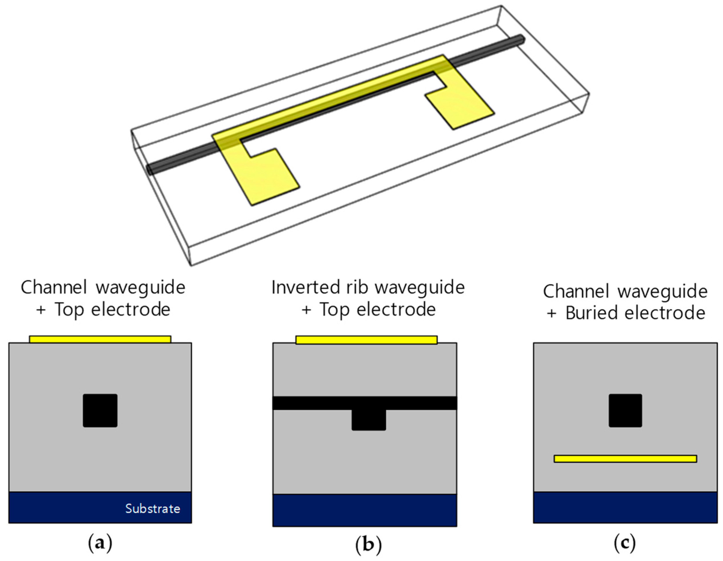
2. Device Design
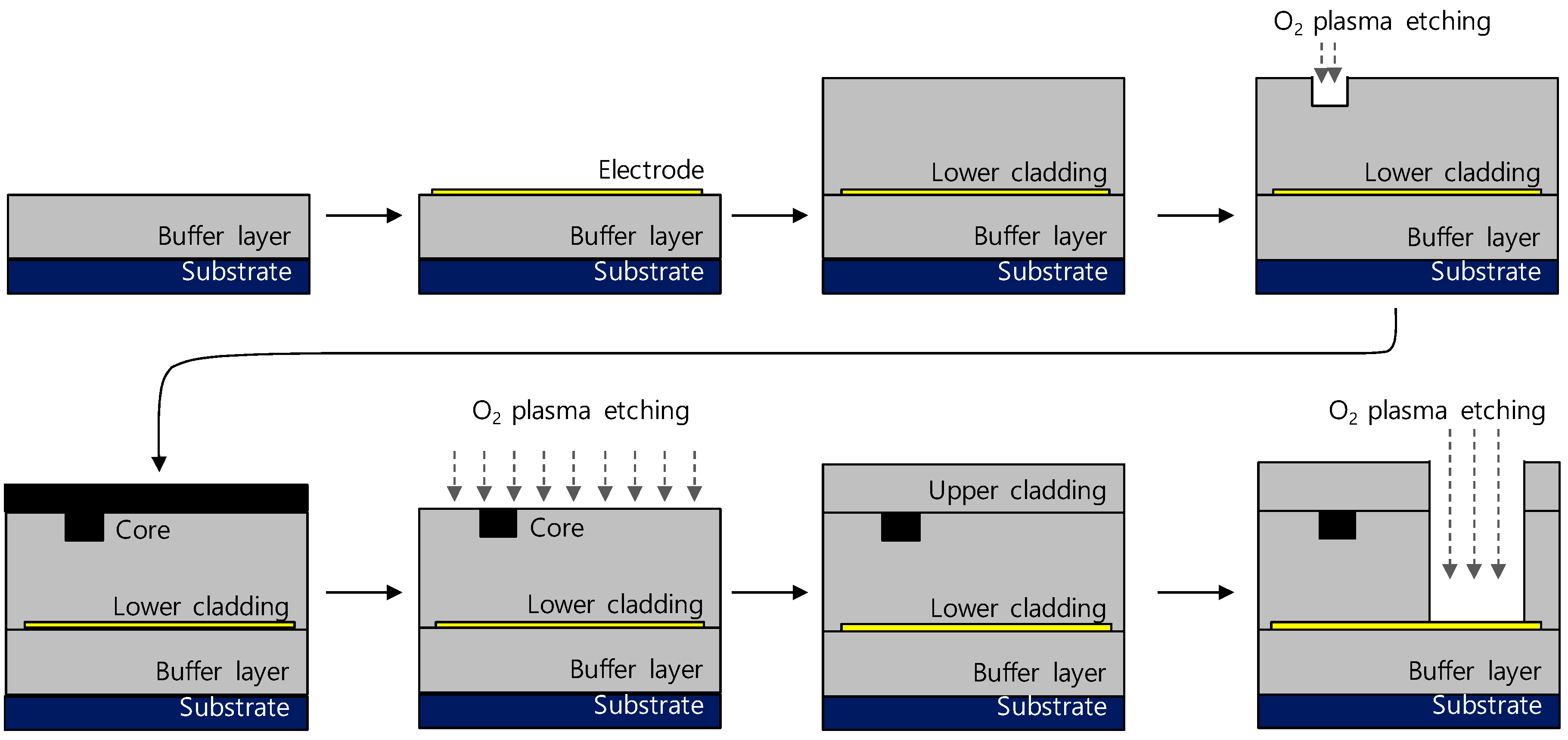
3. Fabrications of the Devices
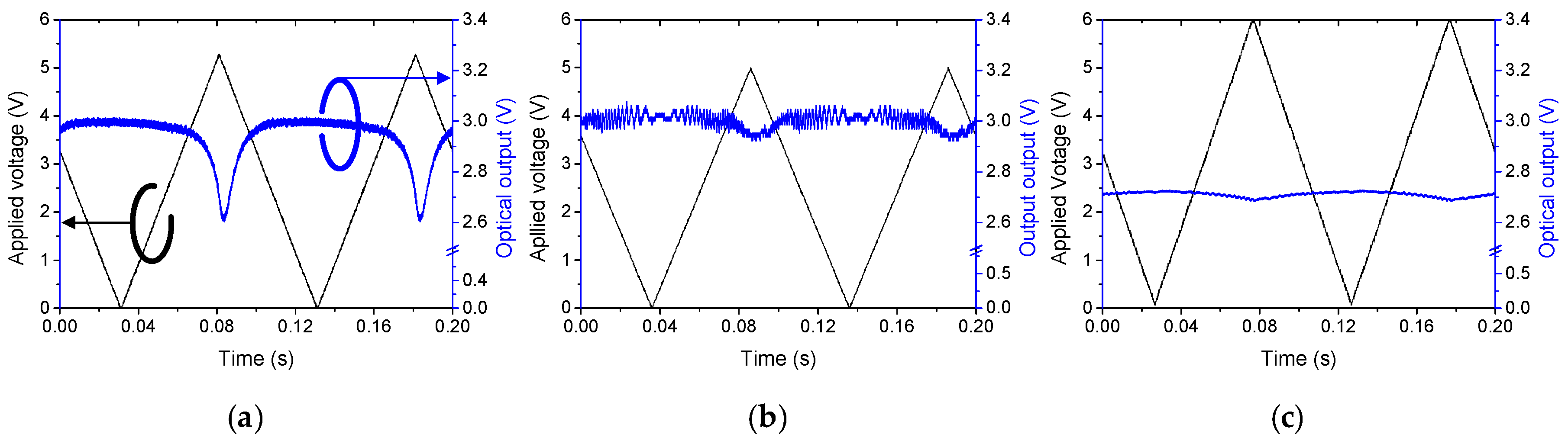
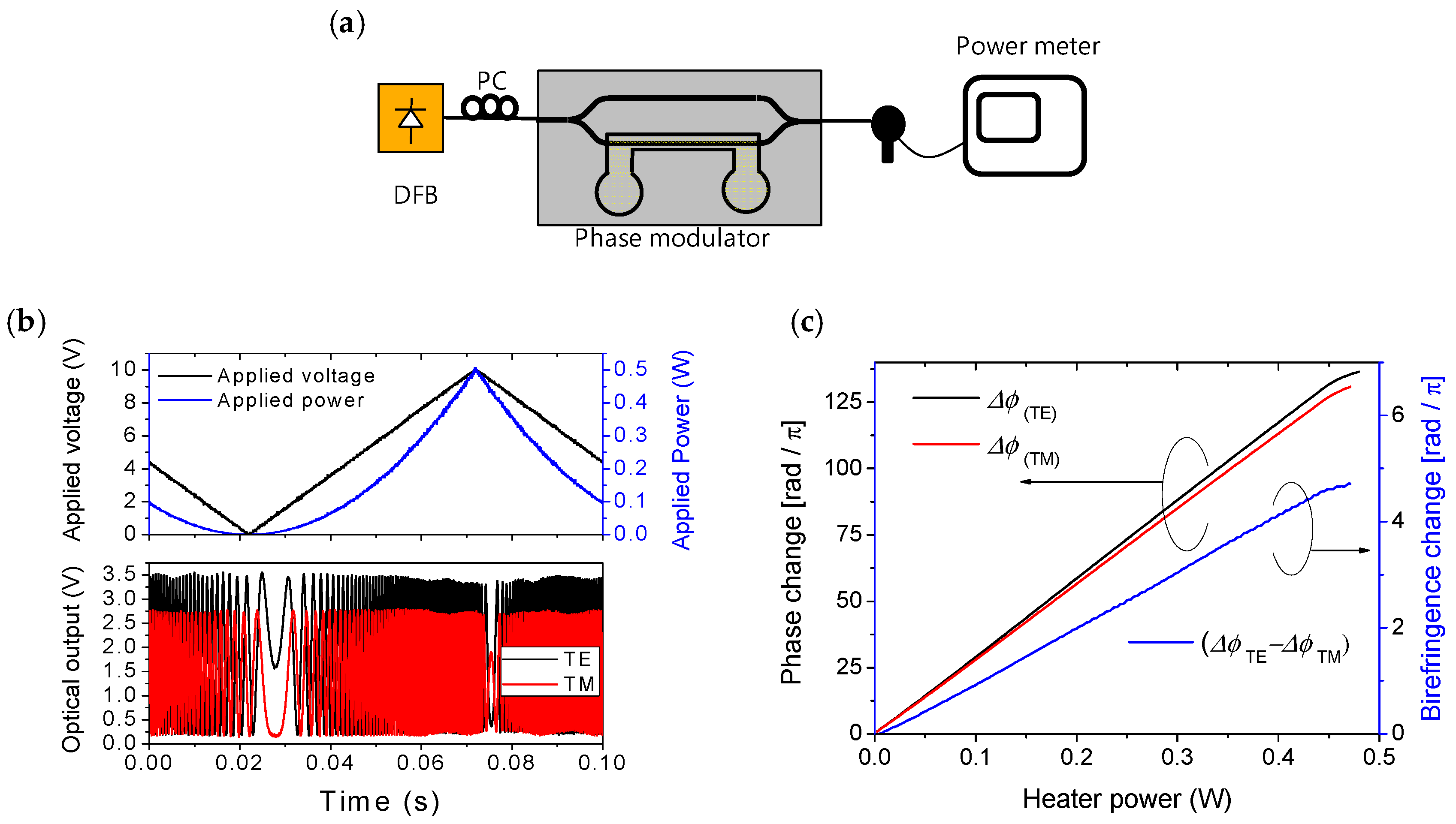
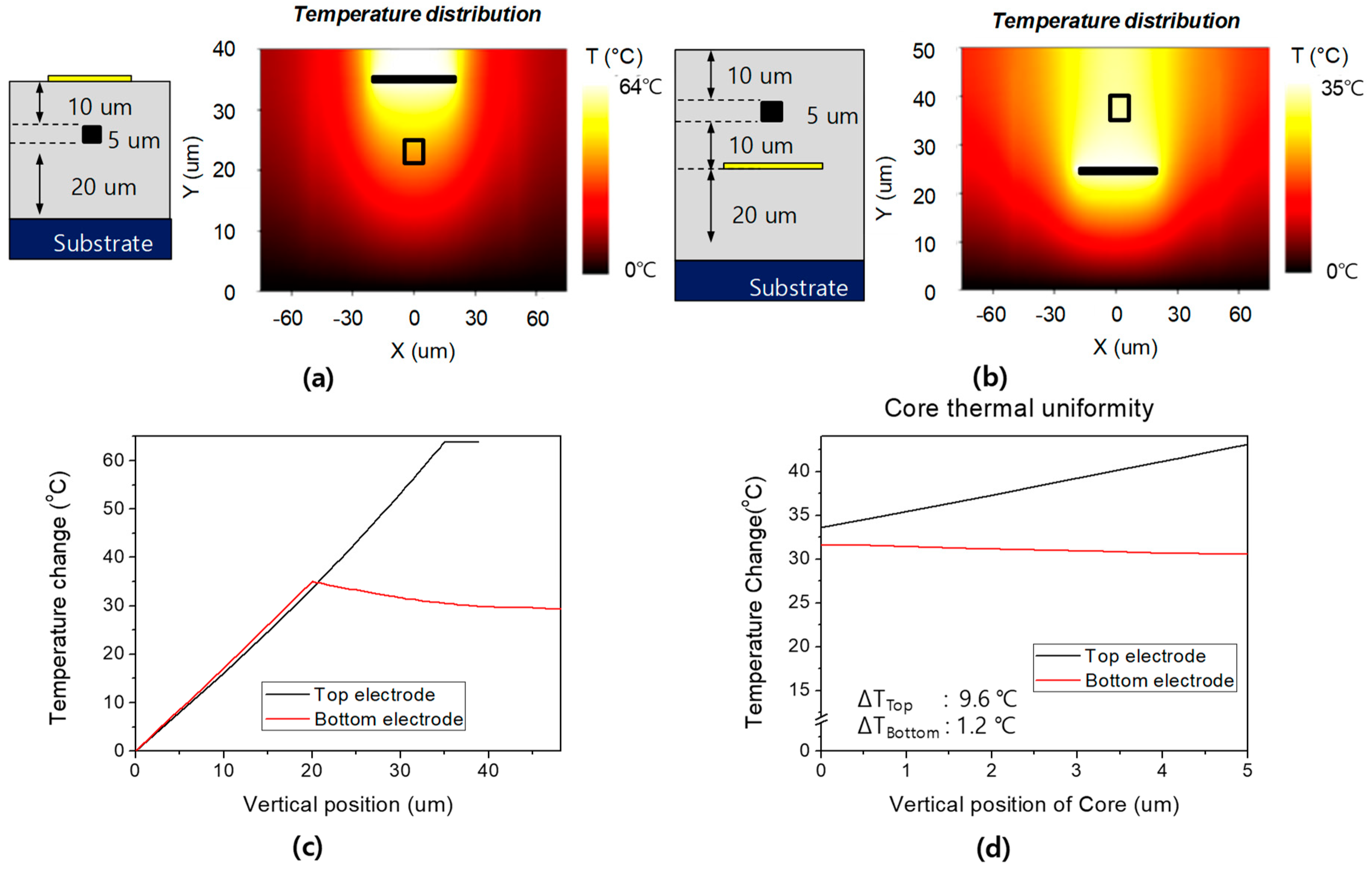
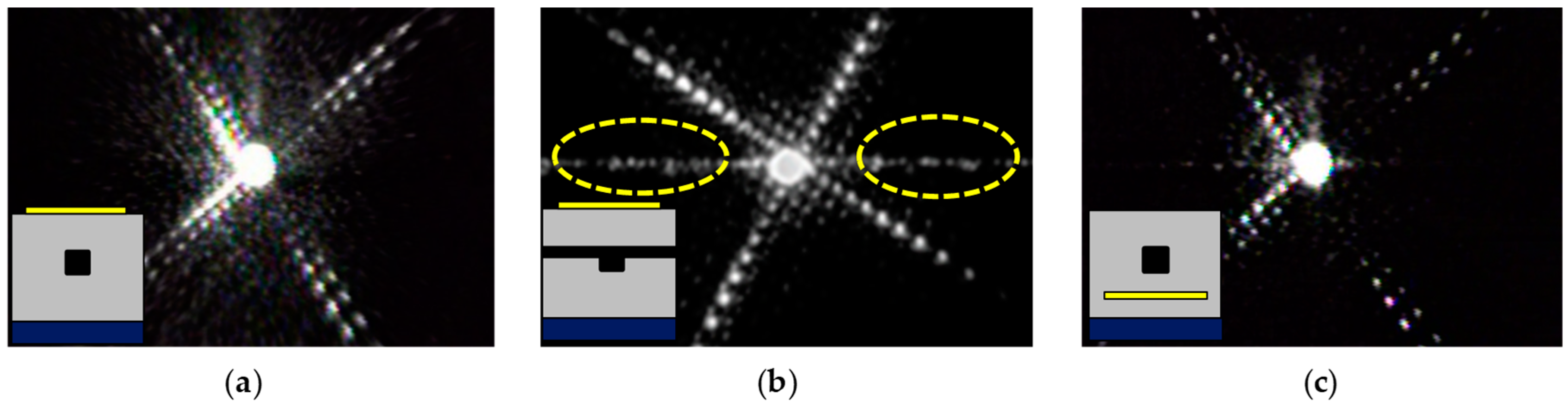
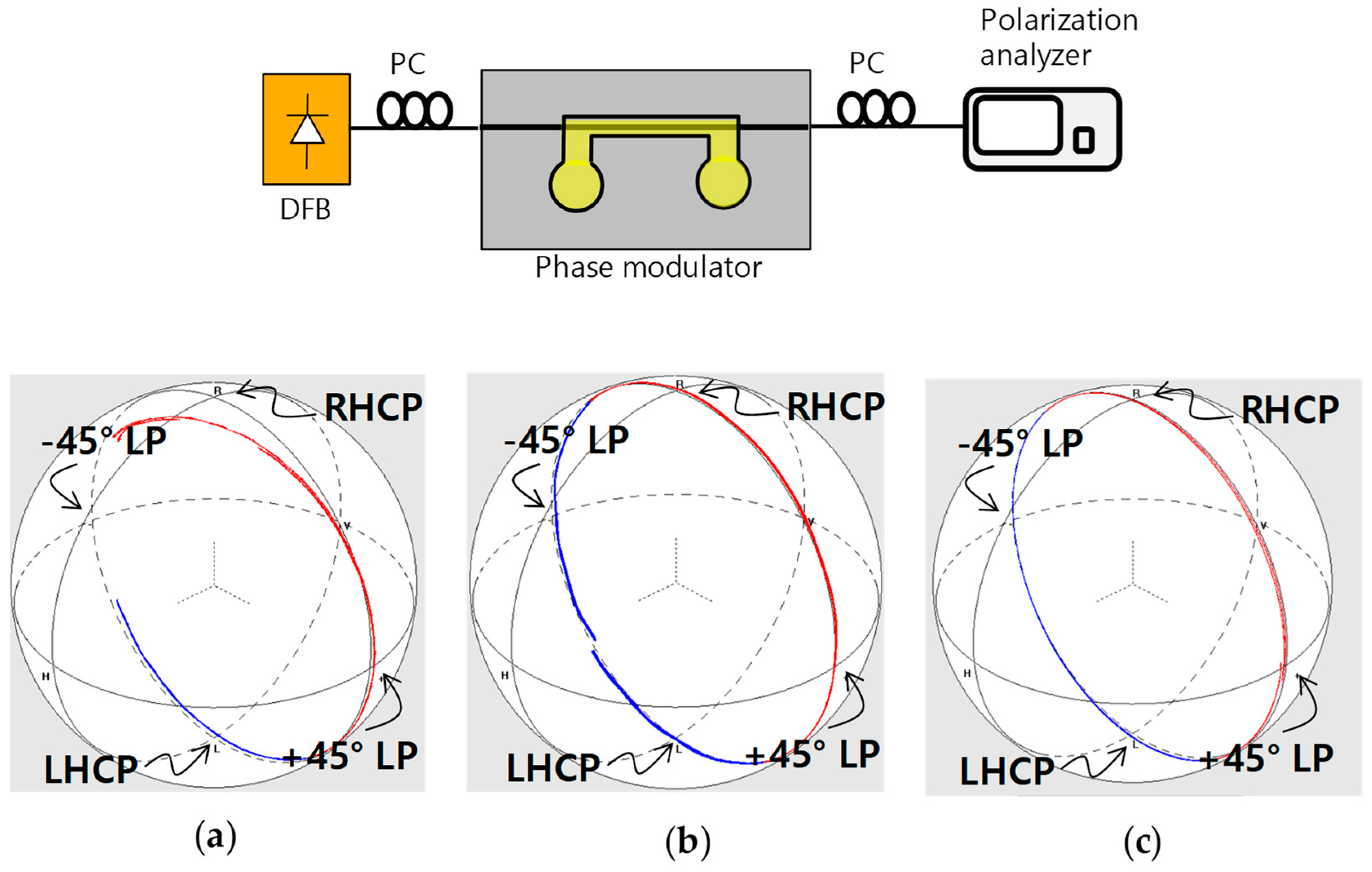
4. Characterization
5. Conclusions
Author Contributions
Acknowledgments
Conflicts of Interest
References
- Kim, S.-M.; Chu, W.-S.; Kim, S.-G.; Oh, M.-C. Integrated-optic current sensors with a multimode interference waveguide device. Opt. Express 2016, 24, 7426–7435. [Google Scholar] [CrossRef] [PubMed]
- Melati, D.; Waqas, A.; Mushtaq, Z.; Melloni, A. Wideband integrated optical delay line based on a continuously tunable Mach-Zehnder interferometer. IEEE J. Sel. Top. Quantum Electron. 2018, 24, 1–8. [Google Scholar] [CrossRef]
- Margallo-Balbas, E.; Pandraud, G.; French, P.J. Thermo-optical Delay Line for Optical Coherence Tomography. In Proceedings of the SPIE International Symposium on Optomechatronic Technologies, Lausanne, Switzerland, 10 October 2007. [Google Scholar]
- Von Poulton, C.; Yaacobi, A.; Cole, D.B.; Byrd, M.J.; Raval, M.; Vermeulen, D.; Watts, M.R. Coherent solid-state LIDAR with silicon photonic optical phased arrays. Opt. Lett. 2017, 42, 4091–4094. [Google Scholar] [CrossRef] [PubMed]
- Frigyes, I.; Seeds, A.J. Optically generated true-time delay in phased array antennas. IEEE Trans. Microw. Theory Tech. 1995, 43, 2378–2386. [Google Scholar] [CrossRef]
- Souza, M.C.; Grieco, A.; Frateschi, N.C.; Fainman, Y. Fourier transform spectrometer on silicon with thermo-optic non-linearity and dispersion correction. Nat. Commun. 2018, 9, 665. [Google Scholar] [CrossRef] [PubMed]
- Harris, N.C.; Ma, Y.; Mower, J.; Baehr-Jones, T.; Englund, D.; Hochberg, M.; Galland, C. Efficient, compact and low loss thermo-optic phase shifter in silicon. Opt. Express 2014, 22, 10487–10493. [Google Scholar] [CrossRef] [PubMed]
- Roeloffzen, C.G.; Zhuang, L.; Taddei, C.; Leinse, A.; Heideman, R.G.; van Dijk, P.W.L.; Oldenbeuving, R.M.; Marpaung, D.A.I.; Burla, M.; Boller, K.J. Silicon nitride microwave photonic circuits. Opt. Express 2013, 21, 22937–22961. [Google Scholar] [CrossRef] [PubMed]
- Sun, Y.; Cao, Y.; Wang, Q.; Yi, Y.; Sun, X.; Wu, Y.; Wang, F.; Zhang, D. Polymer thermal optical switch for a flexible photonic circuit. Appl. Opt. 2018, 57, 14–17. [Google Scholar] [CrossRef] [PubMed]
- Oh, M.-C.; Chu, W.-S.; Shin, J.-S.; Kim, J.-H.; Kim, K.-J.; Seo, J.-K.; Lee, H.-K.; Noh, Y.-O.; Lee, H.-J. Polymeric optical waveguide devices exploiting special properties of polymer materials. Opt. Commun. 2016, 362, 3–12. [Google Scholar] [CrossRef]
- Noh, Y.-O.; Lee, C.-H.; Kim, J.-M.; Hwang, W.-Y.; Won, Y.-H.; Lee, H.-J.; Han, S.-G.; Oh, M.-C. Polymer waveguide variable optical attenuator and its reliability. Opt. Commun. 2014, 242, 533–540. [Google Scholar] [CrossRef]
- Zhang, Z.; Keil, N. Thermo-optic devices on polymer platform. Opt. Commun. 2016, 362, 101–114. [Google Scholar] [CrossRef]
- Oh, M.-C.; Zhang, H.; Zhang, C.; Erlig, H.; Chang, Y.; Tsap, B.; Chang, D.; Szep, A.; Steier, W.H.; Fetterman, H.R.; et al. Recent advances in electro-optic polymer modulators incorporating phenyltetraene bridged chromophore. IEEE J. Sel. Top. Quantum Electron. 2001, 5, 826–834. [Google Scholar] [CrossRef]
- Liu, A.; Zhang, Z.; Liu, D.; Keil, N.; Grote, N. Thermo-optic simulations of silicon nitride/polymer hybrid waveguides. In Proceedings of the SPIE Optics and Optoelectronics, Prague, Czech Republic, 7 May 2013. [Google Scholar]
- Hida, Y.; Onose, H.; Imamura, S. Polymer waveguide thermooptic switch with low electric power consumption at 1.3 um. IEEE Photonics Technol. Lett. 1993, 5, 782–784. [Google Scholar] [CrossRef]
- Oh, M.-C.; Chu, W.-S.; Kim, K.-J.; Kim, J.-H. Polymer waveguide integrated-optic current transducers. Opt. Express 2011, 19, 9392–9400. [Google Scholar] [CrossRef] [PubMed]
- Kim, J.-H.; Park, S.-H.; Choo, W.-S.; Oh, M.-C. Integrated-optic polarization controllers incorporating polymer waveguide birefringence modulators. Opt. Express 2012, 20, 12443–12448. [Google Scholar] [CrossRef] [PubMed]


© 2018 by the authors. Licensee MDPI, Basel, Switzerland. This article is an open access article distributed under the terms and conditions of the Creative Commons Attribution (CC BY) license (http://creativecommons.org/licenses/by/4.0/).
Share and Cite
Kim, S.-M.; Park, T.-H.; Huang, G.; Oh, M.-C. Optical Waveguide Tunable Phase Delay Lines Based on the Superior Thermo-Optic Effect of Polymer. Polymers 2018, 10, 497. https://doi.org/10.3390/polym10050497
Kim S-M, Park T-H, Huang G, Oh M-C. Optical Waveguide Tunable Phase Delay Lines Based on the Superior Thermo-Optic Effect of Polymer. Polymers. 2018; 10(5):497. https://doi.org/10.3390/polym10050497
Chicago/Turabian StyleKim, Sung-Moon, Tae-Hyun Park, Guanghao Huang, and Min-Cheol Oh. 2018. "Optical Waveguide Tunable Phase Delay Lines Based on the Superior Thermo-Optic Effect of Polymer" Polymers 10, no. 5: 497. https://doi.org/10.3390/polym10050497
APA StyleKim, S.-M., Park, T.-H., Huang, G., & Oh, M.-C. (2018). Optical Waveguide Tunable Phase Delay Lines Based on the Superior Thermo-Optic Effect of Polymer. Polymers, 10(5), 497. https://doi.org/10.3390/polym10050497