Article

Charging of Superconducting Layers in Arrays of Coupled Josephson Junctions for Overcritical Currents

by
Marina Cuzminschi
1,2,† and
Alexei Zubarev
2,3,*,†
1
National Institute for Physics and Nuclear Engineering, Department of Theoretical Physics, P.O. Box MG-6, RO-077125 Bucharest-Magurele, Romania
2
Faculty of Physics, University of Bucharest, Magurele, 077125 Ilfov, Romania
3
National Institute of Plasma Lasers and Radiation Physics, Magurele, RO-077125 Ilfov, Romania
*
Author to whom correspondence should be addressed.
These authors contributed equally to this work.
Crystals 2019, 9(7), 327; https://doi.org/10.3390/cryst9070327
Submission received: 19 April 2019 / Revised: 18 June 2019 / Accepted: 22 June 2019 / Published: 27 June 2019

Abstract

:
In this work, we effectuated the numerical simulations of the phase dynamics of an array of Josephson junctions taking into account the capacitive coupling between the neighboring junctions and the diffusion current in the stack. We observed that, if we increase the coupling and the dissipation parameters, the IV characteristic changes qualitatively from the IV characteristics studied before. For currents greater than the critical one, we obtained an additional branch in the IV characteristics. This branch is characterized by a lower voltage than the outermost one. Moreover, we obtained an additional charging of the superconducting layers in the IV region for currents greater than the critical one. We studied the time evolution of this charging by the means of Fast Fourier Transform. We proved that the charge density wave associated with this charging has a complex spectral structure. In addition, we analyzed the behavior of the system for different boundary conditions, appropriate to different experimental setups.

Graphical Abstract

1. Introduction

Arrays of Josephson junctions (JJs) formed by alternating superconducting and insulating layers are known as perspective elements for superconducting electronics [2,3,4]. The arrays are used for coherent THz radiation emission [5,6,7], quantum computing [8], spin current control [9,10] and parametric amplification of charge traveling waves [11,12,13]. Artificial JJs arrays can be replaced by thin films of layered high- T c superconductors in technological applications [14,15].
The previous investigations of phase dynamics of arrays of intrinsic Josephson junctions were focused in the region of McCumber-Stewart hysteresis [1,16]. The breakpoint region [17,18,19,20,21] (corresponding to the transition of some junction in the array from resistive to superconducting state) was observed in that zone. Previous research proved generation of THz radiation and charge density waves in this region, which can play an important role in some technological applications. Particularly, high sensitivity detectors for THz and hundreds of GHz electromagnetic waves imagining have been designed recently [22,23].
Chaos can be associated with the breakpoint region, which was demonstrated in Reference [24]. The existence of chaos can make harder the implementation of some high precision devices. The LC shunting of the JJ was proposed to modulate its behaviour. The shunting leads to the appearance of an additional branch in the IV-characteristic [25]. In our study, we propose another way to realize branching in the IV-characteristic of the JJs array, which will be described below.
Due to the fact that the thickness of superconducting layers in the high-T c superconductors is of the same order as the Debye screening length, the charging appears in the superconducting layers [26,27,28,29]. The charging for currents lower than the critical one was studied previously. Dynamics of charge oscillations are an important marker for the identification of different branches in the IV-characteristic and have significant influence on the stacks behavior. Particularly, the resonance related hysteresis [27] appears in the IV-characteristic due to the charge oscillations and a significant voltage step occurs in the breakpoint region [30]. The generation of the charge traveling wave in JJ stacks was discussed in Reference [31]. In Reference [27], Yu. M. Shukrinov and M. A. Gaafar studied the resonance related hysteresis in a stack of Josephson junctions for small dissipation parameter values (from 0.05 to 0.3). The resonance related hysteresis consists of the traveling wave branch and the outermost branch and is situated in the current interval between the break point current and the critical current.
In our paper, we extended the study of the behavior of Josephson junctions arrays presented in Reference [27] for high values of dissipation parameters. We focused on the JJs arrays’ behavior for currents greater than the critical one, where the novel features appear. We show that for highly dissipative systems, the charging of the superconducting layers is generated for a wide range of currents. As a result, branching appears for overcritical currents in the IV-characteristic. Similar branching for overcritical currents has been experimentally observed by M. Lyatti, et al., in ultrathin high- T c superconducting YBCO nanowires [32] and nanobridges [33]. Our result was derived from numerical simulations of a stack of coupled Josephson junctions in the framework of a capacitively coupled Josephson junctions with diffusion current (CCJJ + DC) model, described in Section 2.

2. Model and Method

We consider a system of N coupled Josephson junctions, composed of N insulating and N + 1 superconducting layers labeled from 0 to N and junctions are labeled from 1 to N. Each layer is characterized by order parameter Δ l ( t ) = | Δ | e i Θ l ( t ) where Θ l is the superconducting phase parameter. The system is studied in the framework of the CCJJ + DC model [34,35], which is an efficient instrument to investigate phase-dynamics of the arrays of JJs. A more generalized model for the prediction of arrays of Josephson junctions behavior is presented in Reference [36]. This model provides results which are in agreement with previous experiments [17,37]. Particularly, it derives a correct equidistant branch structure and shows the existence of the breakpoint region.
In the CCJJ + DC model, due to the absence of complete charge screening in superconducting layers, the generalized scalar potential appears:
Φ l = ϕ l V 0 d Θ l d t ,
with ϕ l being the scalar potential:
ϕ l = Θ l ( t ) Θ l 1 ( t ) 2 e l 1 l d z A z ( z , t ) ,
where V 0 = ω p 2 e , plasma frequency ω p = 2 e I c C , I c is the critical current and C the capacitance of a Josephson junction. In this case, the generalized Josephson equation takes the form:
2 e d ϕ l d t = V l α ( V l + 1 + V l 1 2 V l ) ,
where V l is the voltage between the lth and ( l 1 ) th superconducting layers. The coupling parameter is given by the formula α = ε r D 2 / ( d S d I ) with d S the thickness of the superconducting and d I the thickness of the insulating layers, r D being the Debay screening length and ε the electrical permittivity of the superconductor [27,35].
The generalized scalar potential is associated with the charge density, which appears on the layers:
Q l = Φ l 4 π r D 2 .
It leads to the appearance of the diffusion current: I d i f = Φ l Φ l 1 I c R .
Therefore, the total current which passes through the system presents the sum of superconducting ( I s = I c l sin ϕ l ), quasiparticle ( I q p = V l R ), displacement I d i s p = C d V l d t and diffusion currents. Moreover, the total current after the summation has the form:
I = I c l sin ϕ l + C d V l d t + 2 e R N d ϕ l d t .
In this case, the JJ array behavior is determined by the second order differential equation generalized from Equation (2) for different boundary conditions written in dimensionless form, which is solved numerically [20]:
2 ϕ l t 2 = l A l l ( I sin ϕ l β ϕ l t )
where A for non-periodical boundary conditions is a matrix given by:
A = 1 + α G α 0 α 1 + 2 α α 0 0 α 1 + 2 α α 0 0 α 1 + α G
The non-periodic boundary conditions correspond to the case when the structure at both ends is connected to normal-metal electrodes [27]. For periodic boundary conditions matrix A has the form:
A = 1 + 2 α α 0 α α 1 + 2 α α 0 0 α 1 + 2 α α 0 α 0 α 1 + 2 α
Time t is normalized to ω p 1 . β is the dissipation parameter of the stack, given by the expression β 2 = / ( 2 e C R N 2 I c ) , where R N is the resistance of the junction in the normal state. Current I is normalized to the critical current I c , and G = γ + 1 , with γ = d S / d S 0 = d S / d S N where d S 0 = d S N the thickness of first and last superconducting layers in the stack includes boundary conditions. We mention that the effective thickness of the boundary layers can be different due to the proximity effect at superconductor-normal metal interface [20,27]. For superconducting electrodes periodic boundary conditions are more suitable.
We used the method described in References [20,27] to implement simulations. To calculate the voltages on each insulating layer, we ran the current from I m i n to I m a x with current steps δ I up and then down. The voltages are calculated using the 4th-order Runge-Kutta method for time interval between T m i n and T m a x for each time step δ t as:
ϕ t = l A l l V l
and then the voltage on the lth junction for a given current value is calculated using formula:
< V l > = 1 T m a x T m i n T m i n T m a x V l d t
The charge density (which later in the text is referred to as charge) between two insulating layers is given by the formula derived from Maxwell’s equation · E = Q / ε ε 0 :
Q l = Q 0 α ( V l + 1 V l )
where Q 0 = ε ε 0 V 0 / r D 2 . Numerical stability was investigated by doubling and dividing by half the step in time, step in current, and the time interval of the simulation.
The innitial version of the simulation code for the first time was presented in Reference [38].

3. Main Results

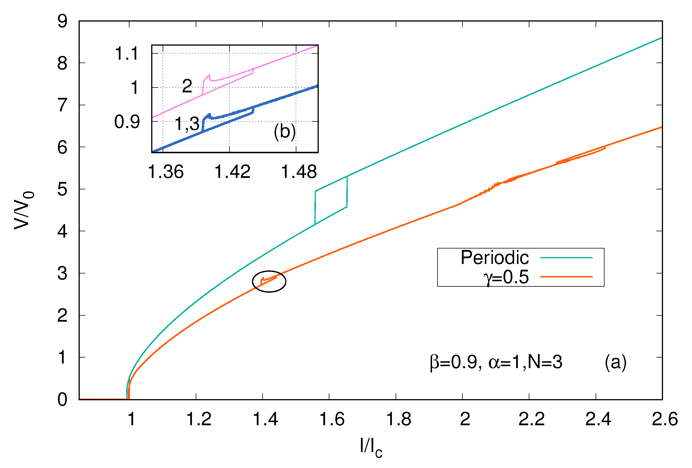
3.1. Appearance of Branching for Overcritical Currents

IV-characteristics for one junction and for the first junction of the stack of three Josephson junctions are presented in Figure 1. Both systems are highly dissipative ( β = 0.9 ). The junctions are strongly coupled ( α = 1 ) in the array of the 3 junctions.
The usual picture is observed for one junction in the stack. Only one branch exists for currents greater then the critical one. However, we can observe branching in the A B C D region (see Figure 1) for currents greater than the critical one for an array of 3 coupled Josephson junctions. For current value I / I c = 1 , the system switches to the resistive state. However the voltage on each junction of the stack is smaller than for a single uncoupled junction. The current gradually increases up till point B, shown in the picture. The spontaneous jump in voltage value, which is highlighted by an increase of about 20 % , occurs (transition from point B to point C). From that point on the voltage is monotonously increasing with the increase of current.
For the decrease of current a new transition from point D to point A occurs with a sudden reduction in the voltage value. From then on, the formation of a small McCumber-Stewart hysteresis can be observed. However, a significant increase of return current can be observed due to strong coupling between the junctions (from I r to I r ). We mention that the IV-characteristic has the same behavior for all junctions in the stack. Significant voltage reduction in the stack can occur due to the modification of charge transport mechanism to a less dissipative one. We suggest studying the appearance of the charging of superconducting layers and generation of charge traveling waves in order to identify it.
The existence of an additional branching for currents greater than the critical one was clearly identified by M. Liatty et al. [32]. From Figure 4 of the mentioned article [32], it can be clearly seen that the voltage jumps similar to the transitions B C and D A from Figure 1 of our article. Because points A and B correspond to different currents, hysteresis appears. M Lyatty et al. observed an additional branch on the IV characteristic of the YBCO nanowires (YBCO is characterized by the lowest distance and the strong coupling between the superconducting lyers) and the study was implemented for higher temperatures, which is in correspondence with high values of the dissipation parameter and is in agreement with our hypothesis about the necessity of strong coupling and high values of the dissipation parameter. Small differences between the form of simulated and experimental IV characteristics result from the finite width of YBCO nanowires and its imperfect crystalline structure.

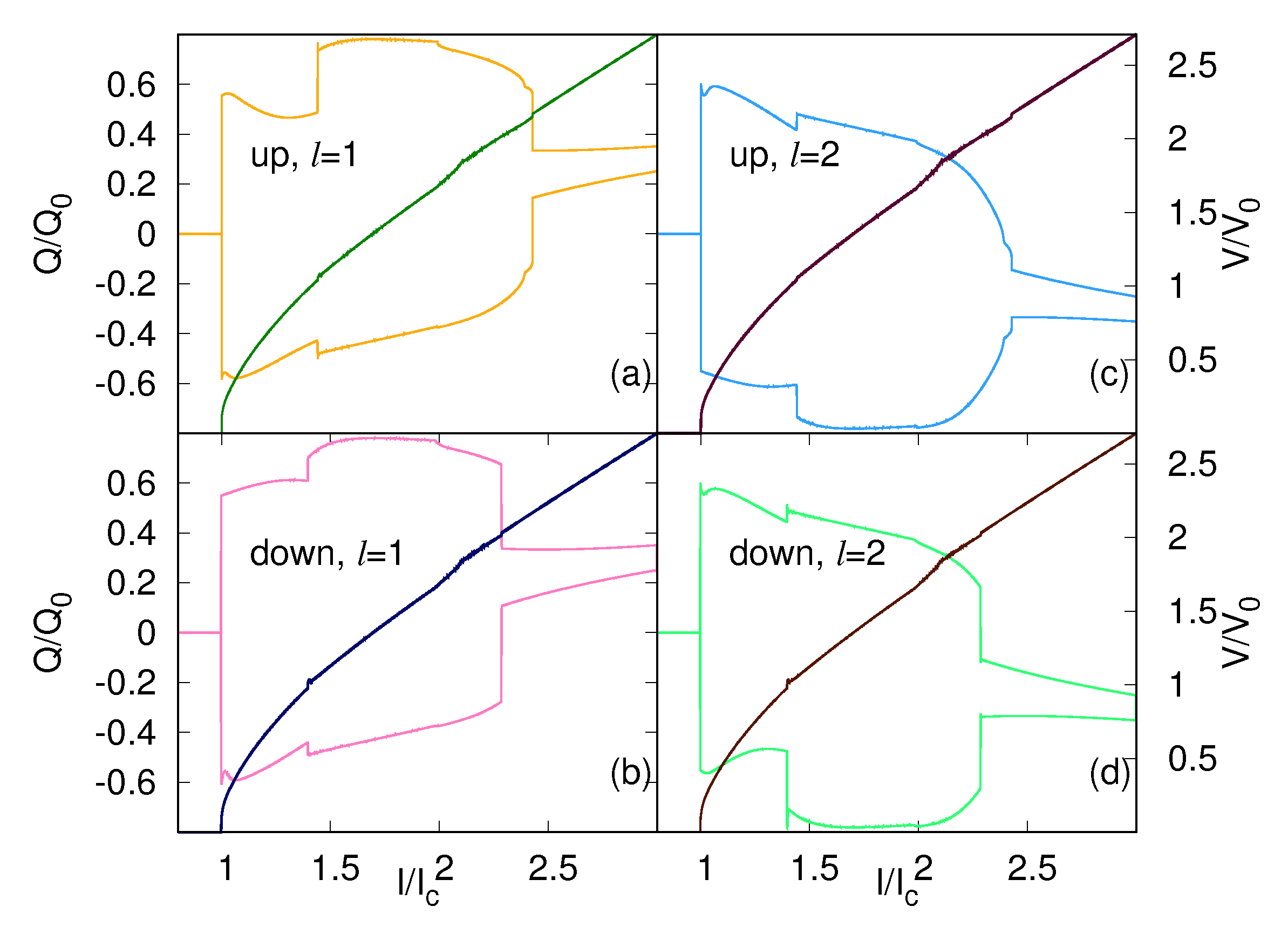
3.2. Charging of the Superconducting Layers

We study charge temporal dependence for superconducting layers in the stack in order to explain changes in the systems’ behavior. We observed the generation of the charge traveling wave for both the increase and the decrease of the current. The amplitude of the charge oscillations and the voltage dependences on current are presented in Figure 2 for both the increase (a) and the decrease (b) of the current. Both phenomena are strongly correlated.
Charge generation (disappearance) is correlated with the voltage jumps and they occur for the same current values. Existence of two distinct branches can be observed: the traveling wave (TW) branch and the outermost branch. The traveling wave branch is characterized by lower voltage and significant ( Q / Q 0 > 0.4 ) amplitude of charge oscillations.
For the increase of current, the charge traveling wave appears starting with the critical current and is generated up till the switch to the outermost branch. The switch occurs at the outermost switching current ( I o ) shown in the picture. It corresponds to label B in Figure 1. For the decrease of current (shown in Figure 2b), the transition from the outermost branch to the TW branch occurs at wave switching current ( I w ), which corresponds to label A in Figure 1. The charge is generated up till the return current. In this way the charging is present in the current region ( I c , I o ) for the increase of current, while for the decrease of current in the region ( I r , I w ) . The charge is generated up to the return current.
The significant voltage reduction for TW branch in comparison with the outermost branch shows that the charge traveling wave is an efficient mechanism for charge transport. We mention that appearance of a more efficient collective transport mechanism in presence of high dissipation was observed for many complex and coupled systems due to self-organization [39]. The charge traveling wave can be observed in JJs arrays with low dissipation [31]; however, in that case the difference in voltage of TW and outermost branches is much smaller. In this way, we have found the origin of branching in the IV-characteristics.
The charge traveling wave temporal dependences for the value of current I / I c = 1.3 are presented in Figure 3a,c for the increase of current and for the decrease of current correspondingly. The selected current value from the phase dynamics is a typical point from the TW branch, and is characterized by a slow variation of the charge oscillations amplitude and is situated far from transient regions. The Fast Fourier Transforms (FFT) analysis was performed due to unharmonious profiles of the waves for both cases and they are presented in Figure 3b,d. FFTs have been effectuated to characterize the frequency of charge dynamics. The main harmonic ( ω / ω p 1 ) can be observed along with subharmonics ( ω / ω p 2 and ω / ω p 4 ).
The relation ( ω / ω p 1 ) shows the existence of resonance between plasma and Josephson oscillations according to Reference [27]; however, a finite ratio of main harmonic and subharmonics amplitudes prevents a permanent increase of charge oscillations amplitude and ensures the TW branch stability.

3.3. The Effect of Number o Junctions in the Stack

Figure 4 presents the dependence of the IV-characteristic on the number of JJs in the array. In the system, branching appears in the overcritical currents region for a number of junctions greater or equal to two ( N 2 ). It consists of the traveling wave and the outermost branches. Detailed study shows that all junctions in the stack in the novel region have the same behavior and formation of the hysteresis represents a collective phenomenon. The IV-characteristics are presented in Figure 4 only for selected values of the numbers of junctions. The branching still exists even for greater values of N.

3.4. Effects of Boundary Conditions

Moreover, we investigated the effect of boundary conditions on the TW and outermost branches. Our simulation confirms that even for non-periodic boundary conditions branching exists in the system. According to Reference [35], the case of non-periodic boundary conditions corresponds to the situation when high- T c layered superconductor is connected to the normal metal at both ends. However, in this case the voltage value is smaller in comparison with the case of periodic boundary conditions, as can be observed from Figure 5.
Furthermore, the voltage values for different junctions are no longer the same. The IV-characteristics for distinct junctions are shown in the inset of Figure 5. For junctions numbers 1 and 3 voltage values coincide, while for the junction number 2 voltage values are higher for the same values of current.
We studied charging for boundary condition parameter γ = 0.5 (Figure 6), which corresponds to the case when the thicknesses of superconducting layers are d S 0 = 2 d S = d S N . We can observe that every abrupt change in the amplitude of charge oscillations leads to modifications in the IV-characteristics. In comparison with case of periodic boundary conditions, the charge oscillations do not vanish for greater currents.
During the study of the system for non-periodic boundary condition and finite value of γ we observe that the charge oscillation profile is correlated with the jumps on the IV-characteristic, similar to periodic boundary conditions. However, the voltage steps are much smaller and the TW branch is fragmented in some short regions. We conclude that large superconducting electrodes are important to ensure the stability of charge oscillations and efficient collective charge transport.
In comparison with the results presented in Section 3.2, the amplitude of charge oscillations for JJs array surrounded by a normal metal electrodes can suddenly change with small current oscillations. Moreover, the mean value of charge on a selected superconducting layer has a nonzero value in case of nonperiodic boundary conditions.

4. Conclusions

In summary, we have demonstrated that, for currents greater than the critical one, branching is present in the IV-characteristic for stacks of highly dissipative coupled Josephson junctions. We have found the traveling wave branch, which is characterized by the voltage lower than the outermost one. If the systems follow the traveling wave branch, the charging of the superconducting layers appears. The traveling wave branch is stable for currents from the critical current to the outermost switching current. The stability of the traveling wave branch is ensured by the specific spectral structure of charge oscillations and the presence of large superconducting electrodes at the edges of the JJs array associated with periodic boundary conditions. The branching and the generation of a charge traveling wave were observed even for non-periodic boundary conditions corresponding to a JJs array surrounded by the normal metal electrodes but the distance between the different branches is much smaller. We have observed the charging for arrays with a different number of junctions ( N 2 ), including large stacks.

Author Contributions

Conceptualization, M.C.; methodology, M.C.; software, M.C. and A.Z.; validation, M.C. and A.Z.; formal analysis, M.C. and A.Z.; investigation, A.Z.; resources, M.C. and A.Z.; writing–original draft preparation, M.C.; writing–review and editing, A.Z.; visualization, M.C.; supervision, A.Z.; project administration, A.Z.; funding acquisition, A.Z.

Funding

This work was partially supported by the Romanian Ministry of National Education by the contract 16N/08.02.2019 with UEFISCDI.

Acknowledgments

We would like to thank Yu. M. Shukrinov for providing initial version of simulation code for Josephson junctions phase dynamics evaluation in the framework of CCJJ + DC model and helpful discussions.

Conflicts of Interest

The authors declare no conflict of interest. The funders had no role in the design of the study; in the collection, analyses, or interpretation of data; in the writing of the manuscript, or in the decision to publish the results.

Abbreviations

The following abbreviations are used in this manuscript:
JJJosephson junctions
TWTraveling wave
IV-characteristicCurrent voltage characteristic
FFTFast Fourier Transform

References

  1. McCumber, D. Effect of ac impedance on dc voltage-current characteristics of superconductor weak-link junctions. J. Appl. Phys. 1968, 39, 3113–3118. [Google Scholar] [CrossRef]
  2. Weinstock, H.; Nisenoff, M. Superconducting Electronics; Springer Science & Business Media: Berlin, Germany, 2013; Volume 59. [Google Scholar]
  3. Holmes, D.S.; Ripple, A.L.; Manheimer, M.A. Energy-efficient superconducting computing—Power budgets and requirements. IEEE Trans. Appl. Superconduct. 2013, 23, 1701610. [Google Scholar] [CrossRef]
  4. Cassidy, M.; Bruno, A.; Rubbert, S.; Irfan, M.; Kammhuber, J.; Schouten, R.; Akhmerov, A.; Kouwenhoven, L. Demonstration of an ac Josephson junction laser. Science 2017, 355, 939–942. [Google Scholar] [CrossRef] [PubMed] [Green Version]
  5. Clark, T. Experiments on coupled Josephson junctions. Phys. Lett. A 1968, 27, 585–586. [Google Scholar] [CrossRef]
  6. Tilley, D. Superradiance in arrays of superconducting weak links. Phys. Lett. A 1970, 33, 205–206. [Google Scholar] [CrossRef]
  7. Welp, U.; Kadowaki, K.; Kleiner, R. Superconducting emitters of THz radiation. Nat. Photonics 2013, 7, 702. [Google Scholar] [CrossRef]
  8. Ioffe, L.; Feigel’man, M. Possible realization of an ideal quantum computer in Josephson junction array. Phys. Rev. B 2002, 66, 224503. [Google Scholar] [CrossRef] [Green Version]
  9. Kadigrobov, A.; Shekhter, R.; Jonson, M. Quantum spin fluctuations as a source of long-range proximity effects in diffusive ferromagnet-super conductor structures. EPL Europhys. Lett. 2001, 54, 394. [Google Scholar] [CrossRef]
  10. Stoutimore, M.J.A. Non-Sinusoidal Current-Phase Relations in Superconductor-Ferromagnet-Superconductor Josephson Junctions; University of Illinois at Urbana-Champaign: Champaign, IL, USA, 2009. [Google Scholar]
  11. Macklin, C.; O’Brien, K.; Hover, D.; Schwartz, M.; Bolkhovsky, V.; Zhang, X.; Oliver, W.; Siddiqi, I. A near-quantum-limited Josephson traveling-wave parametric amplifier. Science 2015, 350, 307–310. [Google Scholar] [CrossRef]
  12. O’Brien, K.; Macklin, C.; Siddiqi, I.; Zhang, X. Resonant phase matching of Josephson junction traveling wave parametric amplifiers. Phys. Rev. Lett. 2014, 113, 157001. [Google Scholar] [CrossRef]
  13. Davidson, A. Distributed Array of Josephson Devices with Coherence. U.S. Patent 4,344,052, 10 August 1982. [Google Scholar]
  14. Kleiner, R.; Müller, P. Intrinsic Josephson effects in high-T c superconductors. Phys. Rev. B 1994, 49, 1327. [Google Scholar] [CrossRef] [PubMed]
  15. Shimakage, H.; Tamura, Y. Chaotic oscillations in Josephson junctions for random number generation. IEEE Trans. Appl. Superconduct. 2015, 25, 1–4. [Google Scholar] [CrossRef]
  16. Stewart, W. Current-voltage characteristics of Josephson junctions. Appl. Phys. Lett. 1968, 12, 277. [Google Scholar] [CrossRef]
  17. Irie, A.; Shukrinov, Y.M.; Oya, G. Experimental manifestation of the breakpoint region in the current-voltage characteristics of intrinsic Josephson junctions. Appl. Phys. Lett. 2008, 93, 152510. [Google Scholar] [CrossRef] [Green Version]
  18. Shukrinov, Y.M.; Mahfouzi, F.; Suzuki, M. Structure of the breakpoint region on current-voltage characteristics of intrinsic Josephson junctions. Phys. Rev. B 2008, 78, 134521. [Google Scholar] [CrossRef] [Green Version]
  19. Shukrinov, Y.M.; Mahfouzi, F. Branching in current–voltage characteristics of intrinsic Josephson junctions. Superconduct. Sci. Technol. 2006, 20, S38. [Google Scholar] [CrossRef]
  20. Shukrinov, Y.M.; Mahfouzi, F.; Pedersen, N.F. Investigation of the breakpoint region in stacks with a finite number of intrinsic Josephson junctions. Phys. Rev. B 2007, 75, 104508. [Google Scholar] [CrossRef] [Green Version]
  21. Shukrinov, Y.M.; Hamdipour, M.; Kolahchi, M. Effect of interjunction coupling on superconducting current and charge correlations in intrinsic Josephson junctions. Phys. Rev. B 2009, 80, 014512. [Google Scholar] [CrossRef]
  22. Du, J.; Hellicar, A.; Leslie, K.; Nikolic, N.; Hanham, S.; Macfarlane, J.; Foley, C. Towards large scale HTS Josephson detector arrays for THz imaging. Superconduct. Sci. Technol. 2013, 26, 115012. [Google Scholar] [CrossRef]
  23. Holdengreber, E.; Moshe, A.; Mizrahi, M.; Khavkin, V.; Schacham, S.; Farber, E. High sensitivity high Tc superconducting Josephson junction antenna for 200 GHz detection. J. Electromagn. Waves Appl. 2019, 33, 193–203. [Google Scholar] [CrossRef]
  24. Hamdipour, M. Detailed investigation of the bifurcation diagram of capacitively coupled Josephson junctions in high-Tc superconductors and its self similarity. Phys. C Superconduct. Appl. 2018, 547, 66–68. [Google Scholar] [CrossRef]
  25. Shukrinov, Y.M.; Rahmonov, I.; Kulikov, K.; Seidel, P. Effects of LC shunting on the Shapiro steps features of Josephson junction. EPL Europhys. Lett. 2015, 110, 47001. [Google Scholar] [CrossRef]
  26. Machida, M.; Koyama, T.; Tachiki, M. Dynamical breaking of charge neutrality in intrinsic Josephson junctions: Common origin for microwave resonant absorptions and multiple-branch structures in the I-V characteristics. Phys. Rev. Lett. 1999, 83, 4618. [Google Scholar] [CrossRef]
  27. Shukrinov, Y.M.; Gaafar, M. Charging of superconducting layers and resonance-related hysteresis in the current-voltage characteristics of coupled Josephson junctions. Phys. Rev. B 2011, 84, 094514. [Google Scholar] [CrossRef]
  28. Shukrinov, Y.M.; Hamdipour, M. Charge creation and nucleation of the longitudinal plasma wave in coupled Josephson junctions. EPL Europhys. Lett. 2010, 92, 37010. [Google Scholar] [CrossRef]
  29. Machida, M.; Sakai, S. Unified theory for magnetic and electric field coupling in multistacked Josephson junctions. Phys. Rev. B 2004, 70, 144520. [Google Scholar] [CrossRef]
  30. Shukrinov, Y.M.; Mahfouzi, F. Influence of coupling between junctions on breakpoint current in intrinsic Josephson junctions. Phys. Rev. Lett. 2007, 98, 157001. [Google Scholar] [CrossRef] [PubMed]
  31. Shukrinov, Y.M.; Hamdipour, M. The c-axis charge traveling wave in a coupled system of Josephson junctions. JETP Lett. 2012, 95, 307–313. [Google Scholar] [CrossRef] [Green Version]
  32. Lyatti, M.; Wolff, M.; Savenko, A.; Kruth, M.; Ferrari, S.; Poppe, U.; Pernice, W.; Dunin-Borkowski, R.; Schuck, C. Experimental evidence for hotspot and phase-slip mechanisms of voltage switching in ultrathin YBa2Cu3O7−x nanowires. Phys. Rev. B 2018, 98, 054505. [Google Scholar] [CrossRef]
  33. Lyatti, M.; Savenko, A.; Poppe, U.; Dunin-Borkowski, R. High-quality YBa2Cu3O7−x nanobridges fabricated by FIB etching. arXiv 2016, arXiv:1603.03459. [Google Scholar]
  34. Shukrinov, Y.M.; Rahmonov, I. Diffusion current in a system of coupled Josephson junctions. J. Exp. Theor. Phys. 2012, 115, 289–302. [Google Scholar] [CrossRef]
  35. Koyama, T.; Tachiki, M. I-V characteristics of Josephson-coupled layered superconductors with longitudinal plasma excitations. Phys. Rev. B 1996, 54, 16183. [Google Scholar] [CrossRef] [PubMed]
  36. Matsumoto, H.; Sakamoto, S.; Wajima, F.; Koyama, T.; Machida, M. Simulation of I-V hysteresis branches in an intrinsic stack of Josephson junctions in high-T c superconductors. Phys. Rev. B 1999, 60, 3666. [Google Scholar] [CrossRef]
  37. Shukrinov, Y.M.; Mahfouzi, F.; Seidel, P. Equidistance of branch structure in capacitively coupled Josephson junctions model with diffusion current. Phys. C Superconduct. 2006, 449, 62–66. [Google Scholar] [CrossRef]
  38. Shukrinov Yu, M.; Rahmonov, I.R.K.K.V. Application of Numerical Methods for the Study of the Josephson Effect: Textbook; JINR: Dubna, Russia, 2016. [Google Scholar]
  39. Kondepudi, D.; Prigogine, I. Modern Thermodynamics: From Heat Engines to Dissipative Structures; John Wiley & Sons: Hoboken, NJ, USA, 2014. [Google Scholar]
Figure 1. IV-characteristics for a junction for β = 0.9 with the return current I r is shown with a dark blue line and for the first junction in the stack of 3 junctions for β = 0.9 and α = 1 with the return current I r , shown with an orange line. The directions of current are shown with arrows next to the IV-characteristics. Simulations have been done for periodic boundary conditions.
Crystals 09 00327 g001
Figure 2. Dependences on current of voltage (dark color lines), together with minimal and maximal values of charge (light color lines), are shown for the increase (a) and for the decrease (b) of current. The direction of current is shown with arrows. Labels for outermost switching and the wave switching currents are shown next to the corresponding current values.
Crystals 09 00327 g002
Figure 3. Charge traveling wave for the first, second and third superconducting layers are presented for current value of I / I c = 1.3 for the increase (a) and the decrease (c) of current. Corresponding results of Fast Fourier Transform (FFT) analysis are presented in (b,d).
Crystals 09 00327 g003
Figure 4. The I-V characteristics for the JJs arrays with different number of junctions in the stack N and the same dissipation of β = 0.8 and the coupling of α = 1 . The branching (for arrays with N 2 junctions) is put in evidence by dashed ellipses.
Crystals 09 00327 g004
Figure 5. (a) IV-characteristics for a system of 3 junctions in a stack with coupling parameter α = 1 , β = 0.9 and periodic boundary conditions (shown with a green line) and γ = 0.5 (shown with an orange line). (b) Zoom at the IV-characteristic for the region marked by an elipse (currents from 1.36 I c to 1.48 I c ) for junctions 1, 2, and 3.
Crystals 09 00327 g005
Figure 6. Maximal and minimal values of charge (light color lines) on the superconducting layers of the stack for α = 1 , β = 0.9 and γ = 0.5 . For the increase of current (a) on the 1st superconducting layer (c) on the 2nd superconducting layer. For the decrease of current (b) on the 1st superconducting layer ( l = 1 ), and (d) on the 2nd superconducting layer ( l = 2 ). The IV-characteristics for the corresponding direction of currents are presented with dark lines.
Crystals 09 00327 g006

