1. Introduction
Photonic integrated circuits, photonic chips or PICs, are increasingly being used in both optical communications and sensing. PICs consist of waveguides connecting different static or tunable elements such as filters and couplers, which convey several functionalities to the chip [
1].
The manufacture of PIC waveguides conventionally relies on depositing and eliminating thin layers of material using photo-lithographic or electron beam processes. Often it is trivial to choose materials with the desired optical characteristics, e.g., silica and silicon nitride [
2], which lead to cost-effective processes with good adherence between the different materials and acceptable yields. However, considering that electro-optically active elements mismatch the crystalline structure and affect all these features, compromises have to be made. Currently the most employed platforms are silicon-on-insulator (SOI) and indium phosphide (InP) [
3]. InP allows the integration of passive and active (emitting/detecting) devices using a single platform technology [
4], while SOI shares technology with complementary metal-oxide-semiconductors (CMOS) and has outstanding processing control, low-cost and high-volume processing.
Independently of which technology is employed, careful temperature control is often needed for the device to work as desired, since the thermal expansion of the chip and refractive index thermal dispersion affect the device behavior. In fact, local thermal control of elements distributed on a complex chip is a common [
5] and relatively cost-effective way of tuning the elements, as recently illustrated in a reconfigurable photonic mesh [
6]. However, thermal control has several drawbacks, its intrinsically difficult spatial isolation being the most important. Any heated element will over time transfer heat to neighboring elements; the closer the elements—i.e., the higher the degree of integration—the more severe the problem.
An alternative, similarly cost-efficient, tunable element could be a waveguide with liquid crystal (LC) cladding [
7,
8,
9,
10]. LCs are an intermediate state of matter between crystal solids and liquids. The simplest class of these materials, the thermotropic nematics, are typically viscous fluids of rod-shaped molecules [
11]. These elongated molecules tend to arrange themselves in the same direction on a macroscopic scale, leading to fluids with both dielectric and optic uniaxial anisotropy. One may either consider the nematic LC as a fluid with orientational order, or as a crystal with no positional order.
Being fluid, the molecules tend to reorient with any applied field, even with relatively small applied voltages (a few volts per µm), and consequently so does the optical anisotropy (birefringence). Hence, by applying an electric field, one can reorient the LC optical axis (indicatrix) by modifying its optical properties. In most applications, one employs surface conditioning—an alignment layer—to induce a preferred initial—relaxed—orientation, and then applies an electrical field to reorient the liquid crystal. This easy procedure to modify the LC birefringence is the reason for LCs to be heavily applied to displays. In these devices, LCs are typically employed to modify the light state of polarization, allowing the light to be transmitted or not by placing the structure between crossed polarizers.
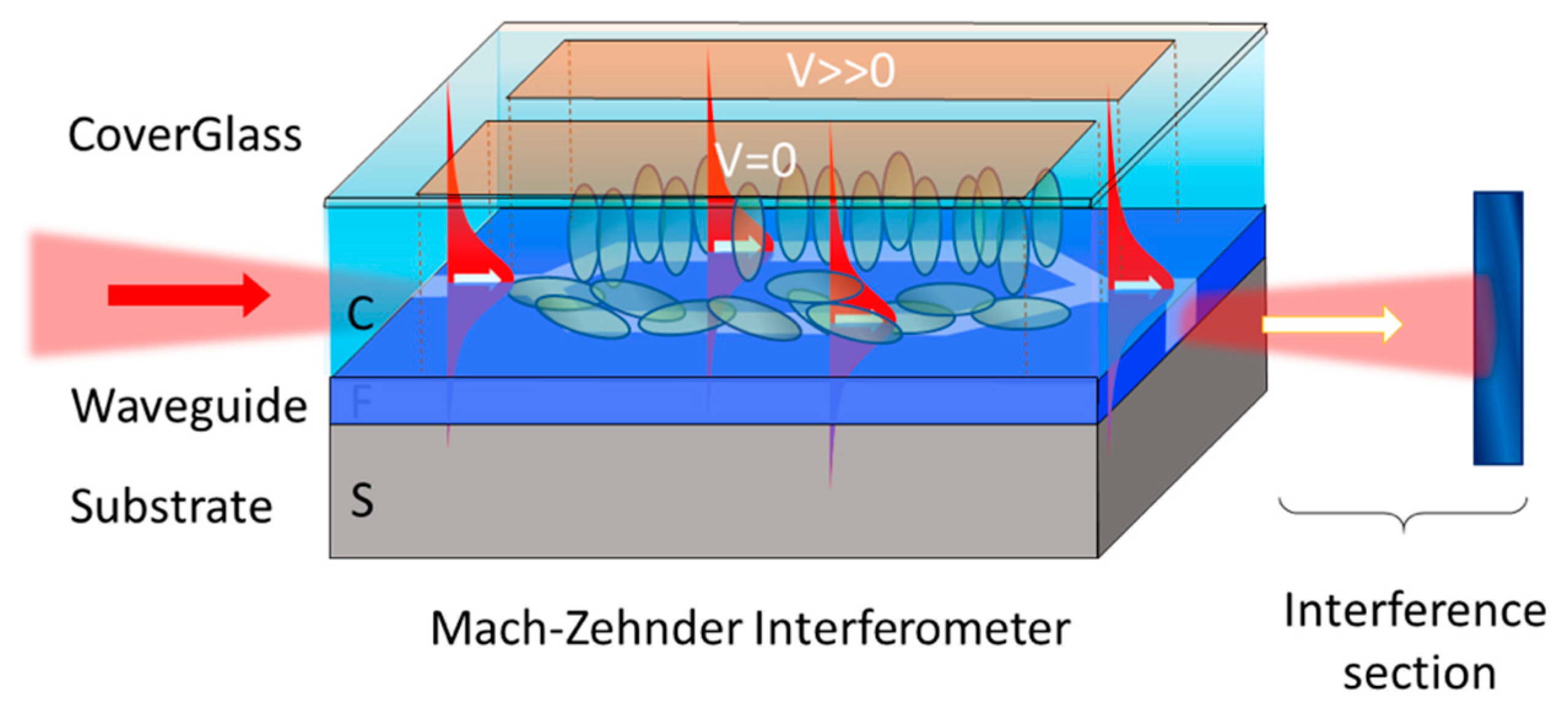
When substituting the conventional silica cladding of a waveguide with LC cladding, the device becomes electrooptically addressable. The effective refractive index of the cladding—as experienced by the light propagating in the core—becomes tunable between the LC ordinary and extraordinary indices (
no and
ne) that affect the propagation of at least one of the polarization modes traveling in the waveguide (
Figure 1).
A great advantage in using LC cladding tuning of the effective refractive index of waveguides is that by employing pixelated devices—like those of LC displays [
12]—customized switching control is trivial. The typical pixel size in high-quality direct-view LC displays is about 100 × 100 µm
2, while in LC on silicon (LCoS) [
13] displays for image projection, the pixel size is about 10 × 10 µm
2. In our facilities, we can adapt the pixel shape and size to any desired design. This allows us to address specific zones of the waveguide selectively. The electric field switching specific LC areas can be confined to µm-sized areas; the reduced thickness of the device avoids spreading of fringing. Hence, by employing pixelated LC devices, one can manufacture reconfigurable PICs with a density limited by the waveguide geometry rather than by the risk of thermal cross-talk between different components. A sandwich structure consisting of a custom designed waveguide structure, a thin LC layer and a generic or custom designed highly pixelated LC counter electrode would allow for the unprecedented complexity and density of the resulting PIC. Only one LC device could cover the entire PIC.
This work shows the first integrated Mach–Zehnder interferometer (MZI) driven by LC in visible (VIS) light. Integrated MZIs are the key tuning elements in the “optical field-programmable gate array (FPGA)” [
6]. MZI LC structures have been presented before in fiber [
14]; however, integrated devices are more stable than conventional or fiber MZIs to ambient thermal changes. Integrated MZIs are typically used as phase shifters, but they are becoming important modules (basic structures) for VIS light in (bio-)sensing or metrology. Moreover, considerable progress in nanophotonics has been focused on this spectral region [
15,
16].
2. Materials and Methods
The waveguide structure was designed and manufactured as a part of the Photonic Chip Design Training course (Valencia, Spain, 2016) [
17]. It was fabricated by the laser direct write (LDW) technique. The platform is based on a 4” silicon wafer that is 500 µm thick, 2.5 µm thermal oxide bottom cladding, 300 nm silicon nitride core and 2 µm top cladding. A Heidelberg DWL 66FS was used for lithography writing. Deposition of the core was conducted by low pressure chemical vapor deposition (LPCVD). The top cladding was deposited by plasma-enhanced chemical vapor deposition (PECVD).
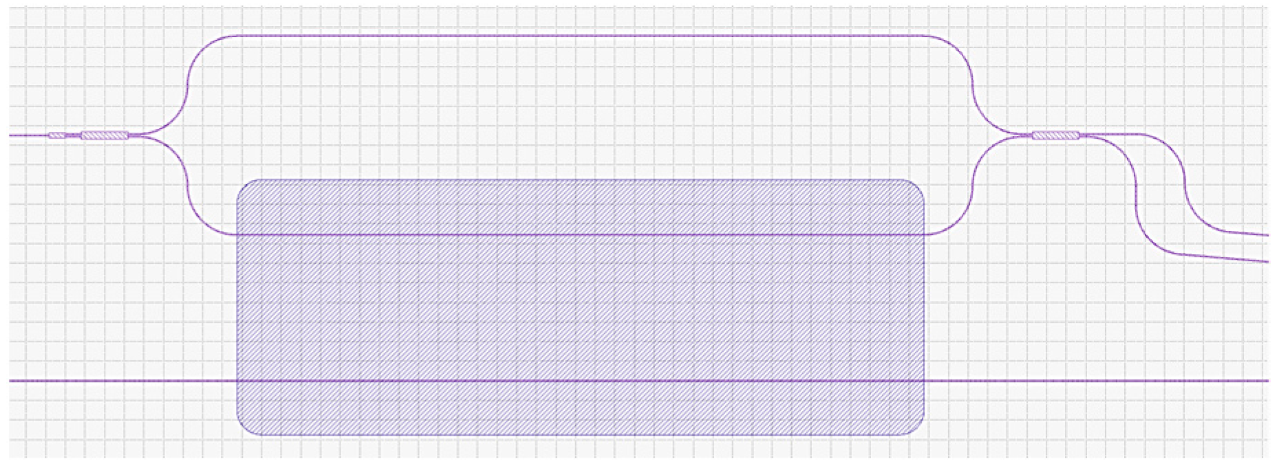
The integrated Mach–Zehnder interferometer (MZI) has a structure similar to any macroscopic MZI. The device consists of three sections; the first splits the input light power into two 50/50 channels. It is made of a 1 × 2 multimode interference (MMI) coupler with a length that couples exactly one half of the power into each output port (at 1550 nm). The second section consists of two parallel waveguides; differences in optical path length can be generated by changing the refractive index by heating [
18] or electrically controlled tunable cladding. In the actual implementation, only one of the two interferometer arms is exposed to the tunable LC refractive index (
Figure 2). The third section, where the interference arises, is a 2 × 2 MMI coupler that recombines light and sends it to one or the other output port depending on the phase delay difference between the arms. The two exiting waveguides are brought to the chip edge for monitoring. The waveguide dimensions were 0.3 µm × 0.6 µm, and the 1 × 2 MMI coupler and the 2 × 2 couplers were generated using the foundry recommendation for a wavelength of 1550 nm. The 50 µm curvature radii were used [
19]. If SiO
2 cladding had been used, this design would ensure a single mode cut-off at 870 nm in the waveguides and dual mode behavior in the MMIs; however, when employing liquid crystal cladding, the cut-off depends on the switching state.
The 6 µm thick LC cell was made by sandwiching the LC material (Merck MDA-98-1602,
no = 1.52,
ne = 1.78) [
20] between the waveguide and an indium-tin-oxide (ITO) coated glass cover. The desired thickness was obtained using a 6 µm thick Mylar film between the chip and the glass cover.
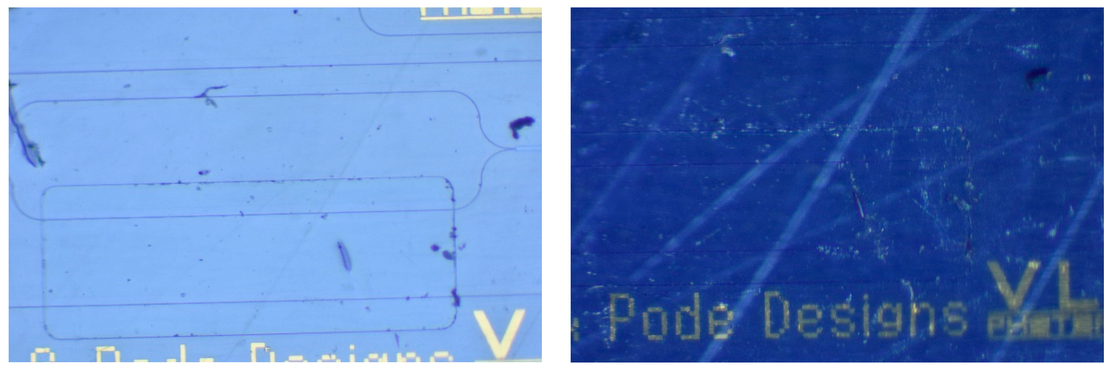
In order to condition the alignment direction, the waveguide was gently rubbed with a velvet cloth, and the glass cover was spin-coated with polyimide [
21] (PIA-2304, LixonAligner), which was likewise rubbed with the velvet cloth in the same direction.
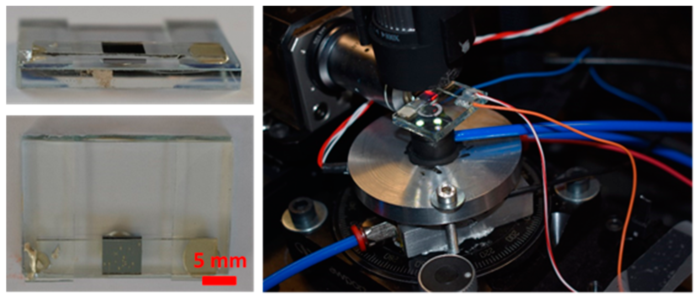
Prior to assembly, the chip was mounted on a glass substrate for easy handling, the cover was precisely located and the cell was filled with the LC using capillarity. The sample was placed on a thermally stabilized XYZθ stage (
Figure 3).
3. Results and Discussion
The LC cell was excited using a 10 kHz square waveform with amplitude varying from 0 to 80 V. The LC alignment was set parallel to the waveguide.
Figure 4 shows that the alignment was almost perfect.
The variations of LC anisotropy upon reorientation are only experienced by the TM polarization perpendicular to the substrate. Therefore, only the TM mode is expected to vary its coupling ratio between outputs when the LC is switched. The transfer function for the output power of an MZI is , where the sub-indices 1, 2 are the different output ports and refer to the + and − signs in the equation; Pin is the input power.
Regarding the
as a function of voltage, it can be approximated as
[
22], where
dc is a duty cycle that is proportional to the voltage.
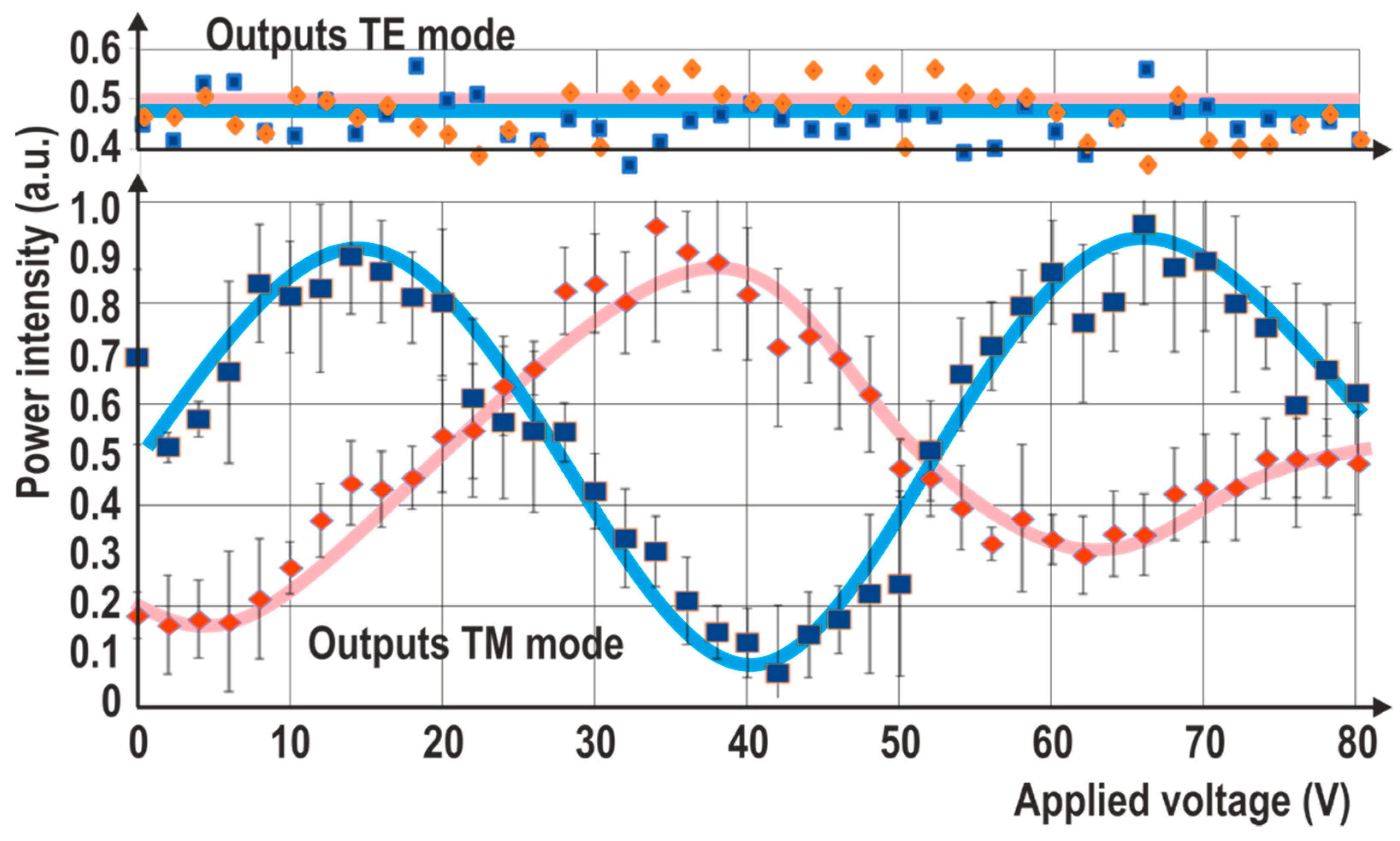
Figure 5 shows the light power at either output waveguide. The TE and TM modes were separated by placing a polarizer at the entrance of the MMI. In red colors (diamonds), one of the outputs (O1) of the MZI is represented. The blue colors (squares) represent the other output (O2). Due to significant noise levels, the data points were averaged over 10 repeated measurements. The errors are provided in vertical bars. The line is a simple spline fit to demonstrate the trend behavior.
Like any MZI, the TM transmission shows a cosine-like variation
. The induced phase variation depends, in a non-linear manner, on the effective refractive variation with the applied field, which can be described as
[
22], and the change in degree of confinement of the traveling mode.
Obviously, the maxima and minima of the curves should match; a small offset between these is attributed to variation in the light coupling, or in scattering caused by the LC. TE transmission is substantially constant upon the whole driving voltage range, as shown by its nearly horizontal trend lines.
The MZI transfer function varies theoretically between zero and a maximum. In our case, residual light is obtained for every applied voltage. This can be clearly seen in
Figure 6, where the maxima for either channel have been shown. In neither case is full extinction achieved.
This is because the MMIs were designed for 1550 nm, as mentioned above, and not for the 632.8 nm working wavelength. Only by a perfect 50/50 power recombination in the output ports can full extinction be achieved. The designed MMIs led to a 63/37 power splitting for 632.8 nm light, leading to a theoretical extinction ratio of −5.6 dB. The discrepancy between the design and characterization wavelength is due to incompatibility between the available production development kits (PDK) necessary for the PIC production and the sample characterization tools available in our installations.
The relatively high voltages needed for full power switching were applied between the silicon substrate and the counter electrode. Hence, most of the voltage drop took place over the silicon-oxide and -nitride layers, rather than over the active LC layer. In future devices, the necessary voltages can be reduced by employing in-plane switching electrodes to a much more reasonable 3–5 V.
4. Conclusions
The results presented here in the VIS spectrum demonstrate that an LC-driven interferometer can be integrated in PICs. These results can be extrapolated to NIR. The LC birefringence generally reduces with increasing wavelength, but at the same time a longer wavelength will be less confined to the waveguide and therefore one should expect the NIR results to be similar, except for residual light. In comparison to MEMS, the pixelated LC offers the possibility of making complex phase devices at a very low price, albeit possibly at the cost of an increased insertion loss. As a standalone device, a switch based on LC cladding switching makes little sense.
The results show that the change in the LC switching state can be used for tuning the effective refractive index experienced by polarized light traveling in a waveguide. Hence, LC cladding may be employed as an alternative to thermal tuning, or in more involved applications as a substitute for conventional phase modulators such as LiNbO3. Obviously, the use of LCs would be restricted to applications where response time is not an issue, as one would expect any nematic LC device to have response times in orders of tens of µs to tens or even hundreds of ms depending on the configurations.

 ,
, 


