Article

Impact of Delay Time before Annealing MAI-PbI2-DMSO Intermediate Phase on Perovskite Film Quality and Photo-Physical Properties

Beijing Advanced Innovation Center for Materials Genome Engineering, Research Center for Sensor Technology, Beijing Key Laboratory for Sensor, MOE Key Laboratory for Modern Measurement and Control Technology, School of Applied Sciences, Beijing Information Science and Technology University, Jianxiangqiao Campus, Beijing 100101, China
*
Author to whom correspondence should be addressed.
Crystals 2019, 9(3), 151; https://doi.org/10.3390/cryst9030151
Submission received: 1 March 2019 / Accepted: 8 March 2019 / Published: 14 March 2019
(This article belongs to the Special Issue Advances in Thin Film Solar Cells)

Abstract

:
High-performance perovskite solar cells are strongly dependent on the quality of the perovskite layer. Two-step sequential deposition of CH3NH3PbI3 (MAPbI3) films is widely used to fabricate perovskite solar cells and many factors influence the quality of perovskite films, such as the delay time before annealing the MAI-PbI2-DMSO intermediate phase, which would impact the morphology and photo-physical properties of perovskite thin films. Here, the experimental research indicates that the impact of the delay time before annealing the MAI-PbI2-DMSO intermediate phase on the quality, crystallinity, and photo-physical properties of perovskite film is crucial. During the delay process, the delay time before annealing the MAI-PbI2-DMSO intermediate phase plays an important role in the nucleation process of perovskite grains inside the intermediate phase. With the extension of the delay time before annealing, the quality of the perovskite film deteriorates, thus the photo-physical properties change. We found that after the localized liquid–liquid diffusion of MAI and PbI2, with the extension of the delay time before annealing the MAI-PbI2-DMSO intermediate phase, the nucleation number of the perovskite grains increases and the grain size becomes smaller. Therefore, with the extension of the delay time before annealing, the device performance deteriorates.

1. Introduction

At present, with the development of the photovoltaic industry and the amazing progress of device manufacturing, research on perovskite solar cells has attracted wide interest, and the performance of these devices has improved significantly in the past few years. The efficiency of perovskite solar cells has jumped from 3.8% to 23.7% in the short term. This is due to the excellent optoelectronic properties of perovskite solar cells [1,2,3,4,5,6]. Although there are many challenges, there are still good developments and there are good reasons to believe that these new solar cells may one day contribute to clean power generation [7,8,9,10,11,12].
There are many factors that impact the performance of perovskite solar cells, such as the ability to form high-quality perovskite thin films, which is critical to research and development in this area [4,6]. Most of the research work is directed toward the development of perovskite-based solar cells. The growth and properties of CH3NH3PbI3 are also important for the development of perovskite solar cells. This triggered our motivation to research the two-step sequential solution process for the preparation of CH3NH3PbI3 thin films using bare glass substrates and fluorine-doped SnO2 (FTO)-coated glass substrates [1,10]. There are many research groups that study different variations of the two-step method, such as changing the annealing time of PbI2, or changing the immersion time and concentration of the MAI solution in which the sample grows [13,14]. The formed films were analyzed to determine their crystal structure, morphology, elemental composition, chemical state and physical properties [13]. Differently from previous research, we indicate the impact of the delay time before annealing the MAI-PbI2-DMSO intermediate phase on perovskite film quality and photo-physical properties for solar cells [15]. Since the process time for transferring the samples from the spin coater to a hot plate is the same, we define the delay time as: “The sample is allowed to stand on the spin coater for 0 s, 5 s and 10 s.”
We characterized the surface morphology of perovskite films with different delay times of the MAI-PbI2-DMSO intermediate phase. It was found that when the delay time was 0 s, the perovskite film had large crystal grains and uniform thickness. With the extension of the delay time before annealing, the quality of the perovskite film deteriorates and the photo-physical properties change—leading to the deterioration of the device performance.

2. Materials and Methods

2.1. Materials

Fluorine-doped SnO2 (FTO) substrates were obtained from Yingkou Opv Tech New Energy Co., Ltd. (Yingkou, China, 7–8 Ω/square, 2.2 mm in thickness, 1.5 × 1.5 cm2 in specification). N,N-dimethylformamide (DMF) and dimethyl sulfoxide (DMSO) were purchased from Sa’en Chemical Technology (Shanghai, China) Co., Ltd. Acidic titanium dioxide solution (bl-TiO2), methyl ammonium iodide (CH3NH3I, MAI, Cas No.14965-49-2, white powder in appearance, purity ≥99.5%) and lead(II) iodide (PbI2, Cas No. 10101-63-0, yellow crystalline powder in appearance, purity >99.99%) were purchased from Shanghai Mater Win New Materials Co., Ltd. (Shanghai, China). Commercial 2,2′,7,7′-tetrakis-(N,N-dip-methoxyphenylamine)-9,9′-spirobifluorene solution (Spiro-OMeTAD, Cas No. 207739-72-8, yellow powder in appearance, purity ≥99.5%) was purchased from Xi’an Polymer Light Technology Corp. (Xi’an, China) [16,17].

2.2. Device Fabrication

First, we placed a fluorine-doped SnO2 (FTO) substrate in a clean dish, added an appropriate amount of deionized water and detergent to the dish and used ultrasonic vibration cleaners (KQ-100E) to perform ultrasonic cleaning for 20 min. Next, an appropriate amount of absolute ethanol was added to the Petri dish and ultrasonically cleaned for 20 min. Then, an appropriate amount of a mixed solution of isopropyl alcohol, acetone and deionized water in a volumetric ratio of 1:1:1 was added to the culture dish, followed by ultrasonic washing for 20 min. Finally, the cleaned substrate was placed in a UV light cleaner (BZS250GF-TC, Shenzhen Huiwo Technology Co., Ltd., Shenzhen, China) for 15 min.
The high-temperature dense titanium dioxide layer was prepared by spin-coating on an FTO substrate with a high-temperature titanium dioxide-hydrochloric acid spin-coating solution. The spin-coating speed was 2000 rpm and the spin-coating time was 60 s. The spin-coated FTO substrate was placed on a hot plate at 150 °C for 20 min, and then sintered at 500 °C for 30 min in a muffle furnace. In the preparation of the perovskite layer, the PbI2 precursor solution was prepared by dissolving PbI2 in a mixed solution of N,N-dimethylformamide (DMF) and dimethyl sulfoxide (DMSO) (the volume ratio of DMF to DMSO was 0.95:0.05). Finally, a 600 mg/mL precursor solution was formed. A methylammonium iodide (CH3NH3I/MAI) precursor solution was prepared by dissolving MAI in anhydrous isopropanol to form a 70 mg/mL solution. After the solution was prepared, the precursor solution of PbI2 was directly rotated onto the dense layer at a rotating speed of 1500 rpm and a rotating time of 30 s. After stopping the rotation, the precursor solution of MAI was uniformly coated on the unheated PbI2 film. Then the precursor solution was rotated immediately with a rotating speed of 1500 rpm and a rotating time of 30 s. The spin-coated substrate was heated at 150 °C for 20 min. After spinning the MAI solution, the perovskite layer was annealed at 150 °C after a delay of 0 s, 5 s and 10 s at room temperature. The procedure was conducted three times.
The electron-blocking layer was deposited on top of the perovskite layer by 3000 rpm for 30 s using Spiro-OMeTAD solution. Finally, the soot from the burning candle was collected using an FTO glass substrate and used as a sponge-like carbon counter electrodes (CEs). Then, the sponge-like carbon film collected on the FTO glass was pressed against the prepared unfinished device [18].

2.3. Characterization

An X-ray diffractometer (XRD) (D8 Focus, Bruker, Dresden, Germany) was used to obtain XRD spectra from samples of perovskite films deposited on bl-TiO2/FTO substrates. The morphologies of these perovskite films were viewed with a scanning electron microscope (SEM) (SIGMA, Zeiss, Jena, Germany). The photo-current density–voltage (J–V) characteristics were measured under simulated standard air-mass (AM) 1.5 sunlight with using a solar simulator (Sol 3A, Oriel, Newport, RI, USA). All the measurements of the perovskite solar cells were performed under ambient atmosphere at room temperature without encapsulation [14].

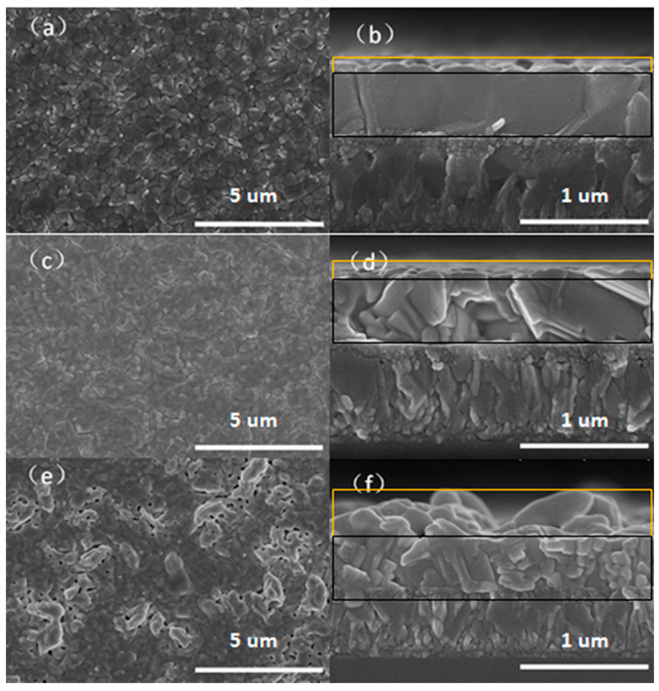
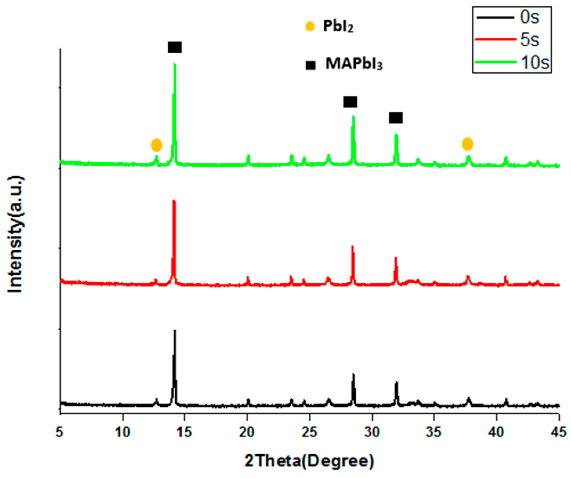
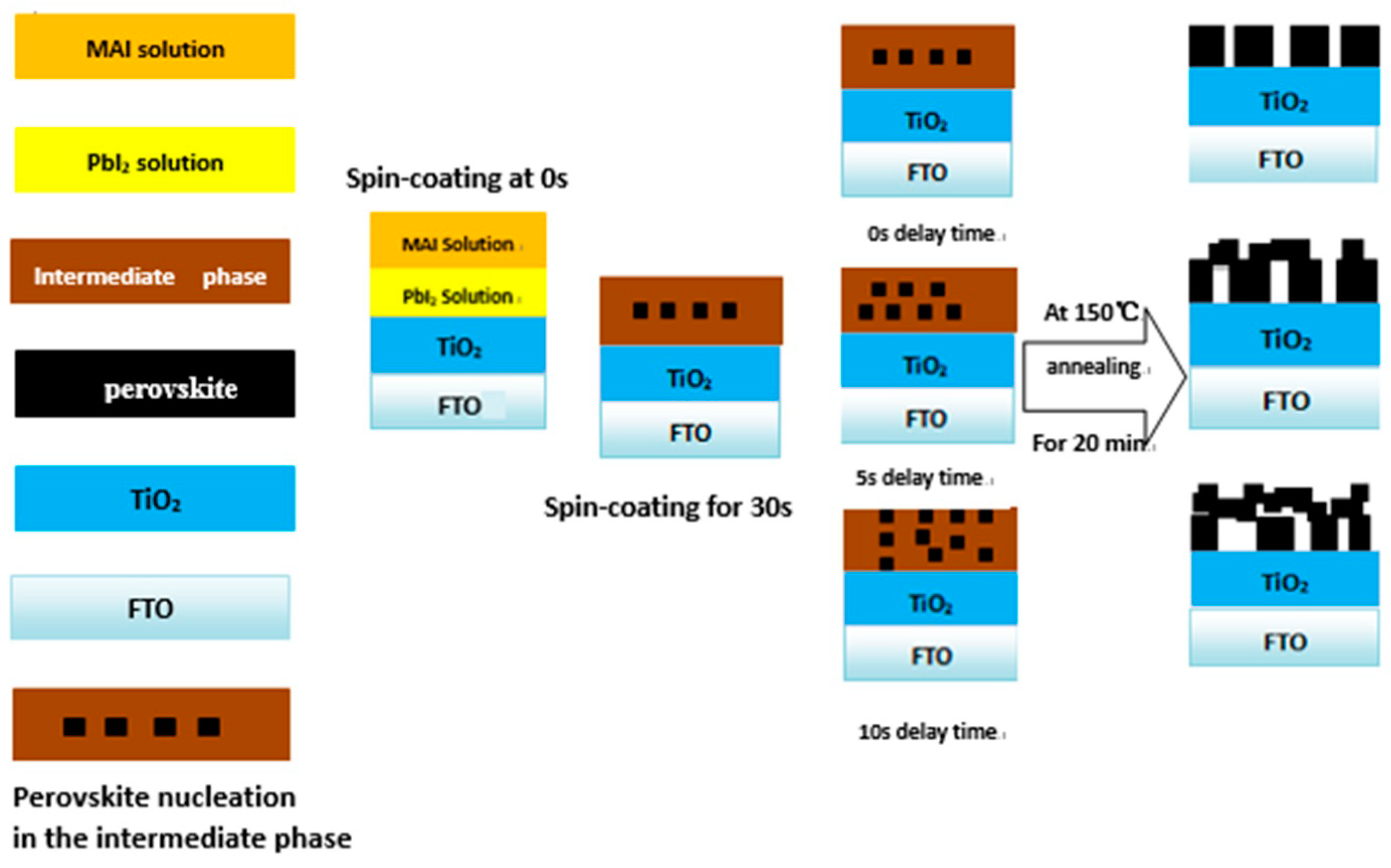
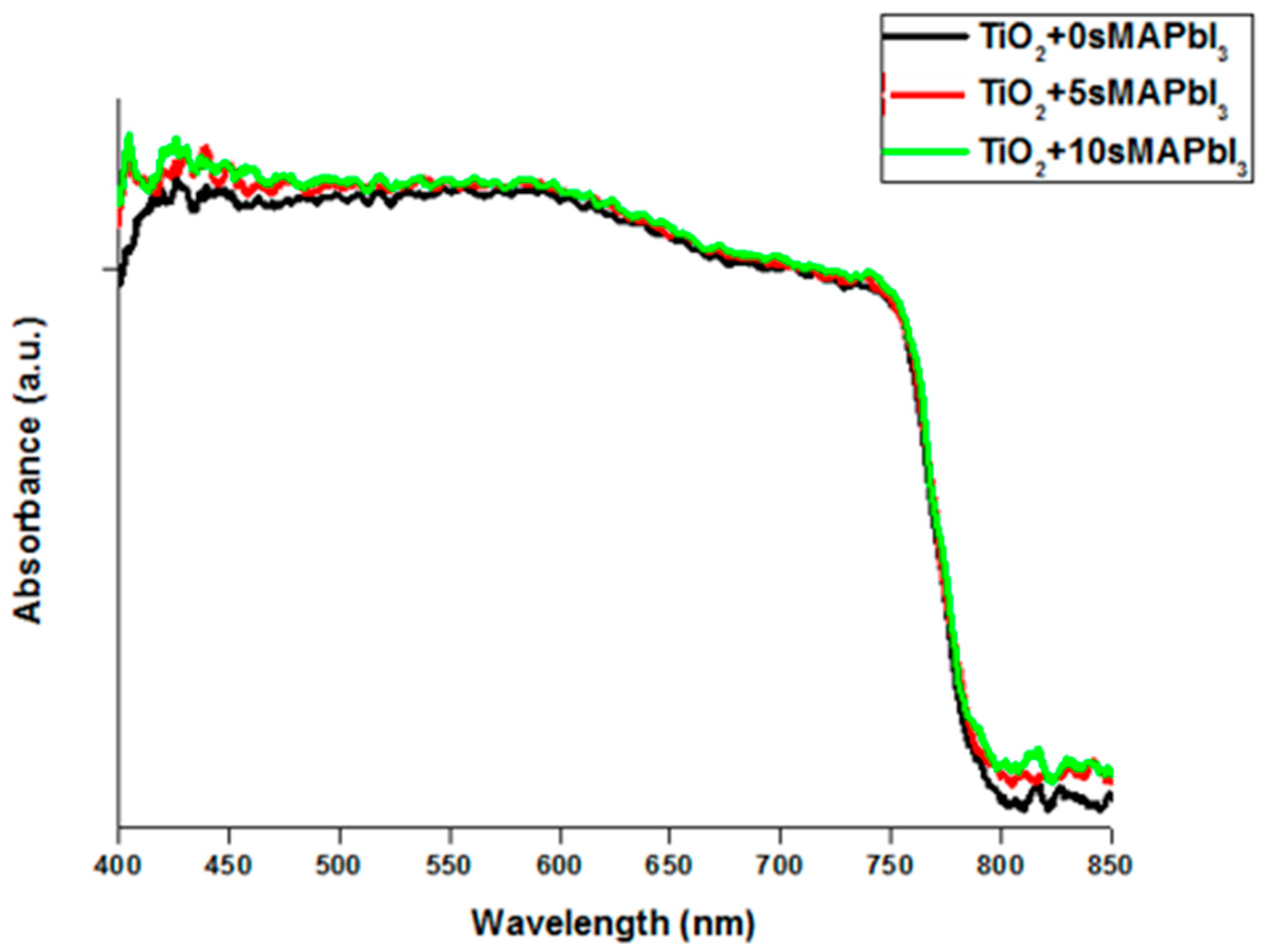
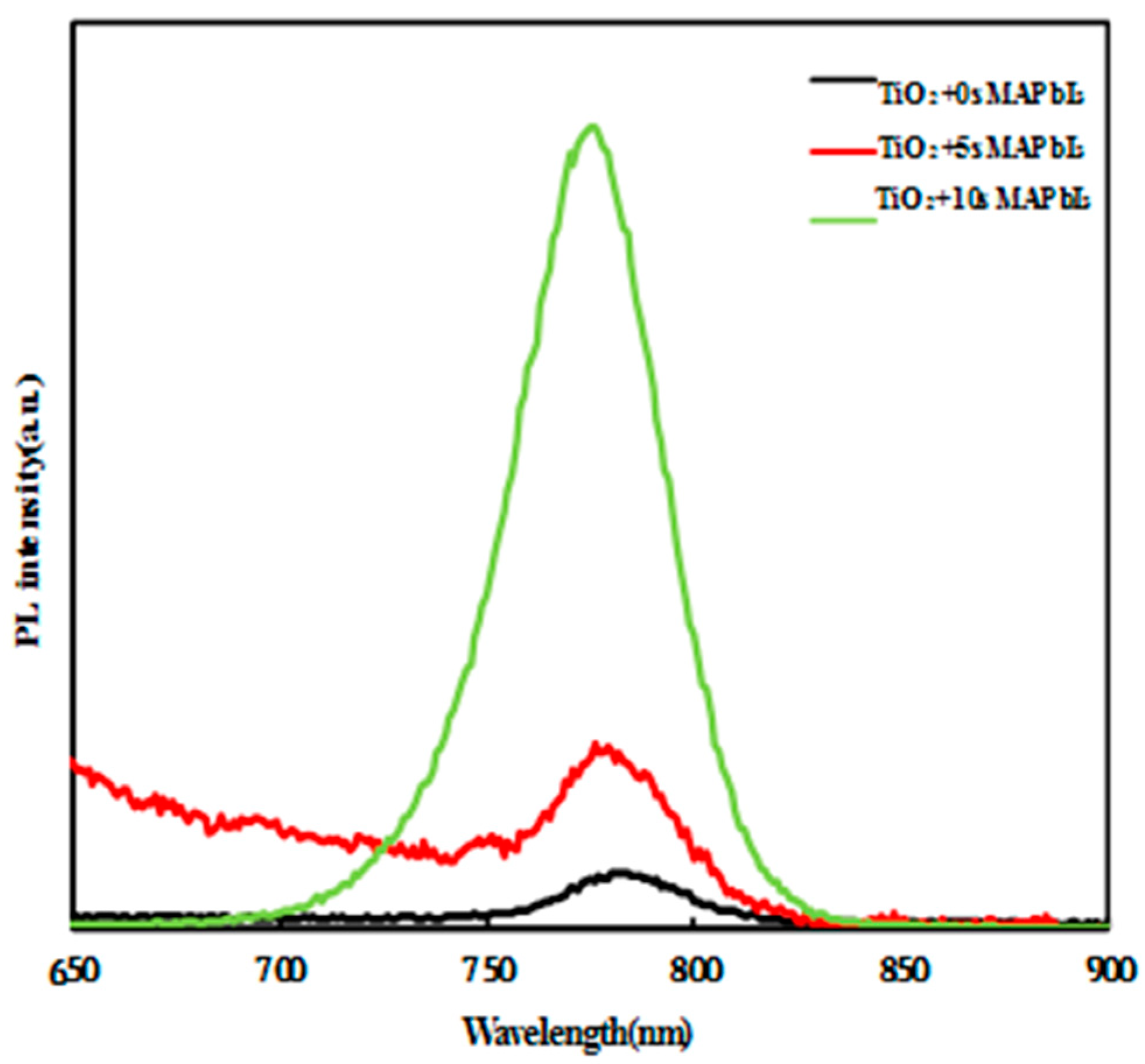
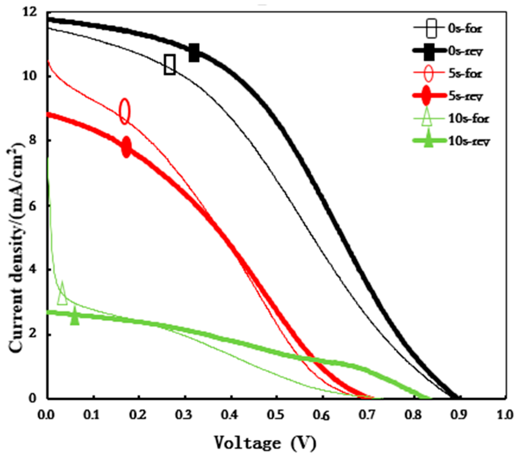
3. Results and Discussion

In this study, the impact of the delay time before annealing on the MAI-PbI2-DMSO intermediate phase on the perovskite solar cells’ films was investigated. Perovskite films with different delay times after the spin-coating of MAI precursor solution, viewed by SEM, are shown in Figure 1. Figure 1a,c,e show the surfaces made with the delay times of 0 s, 5 s, and 10 s. Figure 1b,d,f are cross-sectional views of the 0 s, 5 s, and 10 s films. From Figure 1a, when the delay time is 0 s, the crystal grains of the perovskite are uniform and the grain size is about 400 nm. The perovskite film is dense, without pin-holes and cracks. The cross-section depicted in Figure 1b shows that the thickness of the 0 s perovskite film is very uniform and the film thickness is about 400 nm. We then adjusted the delay from 0 s to 5 s. Thereafter, as shown in Figure 1c, the grain size of the perovskite film is not uniform and the grain boundary is not obvious, so the single grains cannot be distinguished accurately. From the cross-section of Figure 1d, it can be seen that the phenomenon of stacking of perovskite single crystals appeared and the film thickness of about 400 nm consists of many small perovskite crystal particles. In addition, Figure 1e shows that the flatness and uniformity of the film made with the 10 s delay time are significantly worse than the flatness and uniformity of the 5 s film. The surface of the film has large pin-holes, small crystal grains and irregular growth. From Figure 1f—the cross-sectional view—we see that these protrusions actually grow some irregular crystal particles on the top surface of some crystals, resulting in a partial or even multi-layer crystal on the surface of the film, therefore the surface of the film is uneven. According to the above analysis, we conclude that the quality of the film deteriorates with the extension of the delay time before annealing.
Figure 2 shows a typical diffraction pattern selected from XRD experiments normalized to perovskite films with different delay times, showing peaks at 14.19°, 28.50° and 33.5° due to (110), (220) and (222). The crystal plane of perovskite is a tetragonal phase structure [14,19]. We found that the perovskite films made with three different delay times have CH3NH3PbI3 perovskite crystal diffraction peaks. This result indicates the formation of tetragonal phase perovskite crystals. Figure 2 shows that the peaks at 12.56° and 38.54° are attributed to the (001) and (003) reflections of PbI2. The XRD data of PbI2 show a low diffraction intensity of PbI2 (001) at 12.56° and (003) at 38.54° for a 0 s delay. Obviously, the PbI2 peaks of the 5 s and 10 s films are slightly higher than the peaks of the 0 s device, reflecting the presence of more PbI2 residues. The intensity ratios of (003)/(001) for 0 s, 5 s, and 10 s data look more constant.
The precipitation of PbI2, caused by the incomplete reaction of PbI2 and MAI in the crystallization process, impacts the morphology of the perovskite, which corresponds to the results of the SEM topography. With the extension of the delay time before annealing, the growth of perovskite grains is impacted.
According to the analysis of the SEM image and the XRD image, the mechanism of different delay times affecting annealing after spin-coating MAI is shown in Figure 3. During the experiment, the MAI solution was spin-coated immediately after being applied onto the PbI2 solution. During the spin-coating process, it was observed that during the delay time before annealing, the MAI-PbI2-DMSO intermediate phase immediately changed from yellow to dark brown, and after annealing a bright black perovskite film was formed. By comparing different delay times, we found that when the delay time is 0 s, the crystal grains forming the perovskite are relatively large, and the crystal grains are uniform without overlap. With the extension of the delay time before annealing, the grain size becomes smaller, and the phenomenon of stacking will appear, which is consistent with the trend of changes in the SEM images measured for different delay times, indicating that the surface of the film deteriorates with the extension of the delay time before the annealing of the perovskite film. The SEM images show that more nuclei are generated during the drying process, the grain size might be decreases and the stack grows, resulting in an increase in the number and surface roughness of the perovskite film pin-holes [14,20].
The UV-Vis absorption spectra of the absorption spectra of MAPbI3 perovskite films with different delay times are shown in Figure 4. Figure 4 shows that the curve conforms to the light absorption characteristics of a conventional perovskite film. The three perovskite films have relatively strong peaks between 450 nm and 750 nm. It was found that the absorption rate of the 10 s film was slightly higher than that of the 5 s and 0 s films. With the extension of the delay time before annealing, the number of perovskite nucleation increases, impacting the grain size of the perovskite and the flatness of the film. The rough surface of the thin film gives rise to lower reflectivity light, which enhances the absorption rate [21].
Figure 5 shows the photoluminescence spectra of MAPbI3 perovskite films at different delay times on a dense TiO2 layer. We found that the emission peaks of the three perovskite films range from 730 nm to 830 nm. At 0 s, the peak of photoluminescence is low, indicating an increased number of photo-generated carriers injected into the dense TiO2 layer in the perovskite absorption layer. In addition, better carrier quenching is exhibited, which benefits the performance of the perovskite solar cells. With the extension of the delay time before annealing, the intensity of the photoluminescence emission peak also increases, and the number of photo-generated carriers injected into the TiO2 layer decreases. The reason for this is shown in the SEM image. The longer the delay time, the smaller the grain size of the perovskite film, the worse the film quality, and the more defects inside the film, so fewer photo-generated carriers are injected into the dense TiO2 layer in the perovskite absorption layer and the quenching ability of the carriers is weakened [22,23]. We measured significant emissions at 782 nm, 779 nm and 775 nm at 0 s, 5 s and 10 s [24].
With the extension of the delay time before annealing, the perovskite grains become smaller and the grain boundary of the film increases, which leads to the deterioration of the quality of the perovskite film and may affect the ability of the photo-generated carriers to be injected into the TiO2 layer from the perovskite layer. In summary, it was shown that the quality of the perovskite film with a delay time of 0 s is the best [25,26].
As shown in Figure 6, with the extension of the delay time before annealing, the device performance deteriorates, consistent with the film morphology and photo-physical properties. With the extension of the delay time, the quality of the perovskite films and the photo-physical properties change, which leads to the deterioration of the device performance.

4. Conclusions

In summary, it was found in the experiment that the color of the film quickly changed from yellow to dark brown during the spin-coating MAI process. We found that the perovskite nucleation in the intermediate phase formed increased with the extension of the delay time before the annealing of the MAI-PbI2-DMSO intermediate phase. From the SEM image, it was seen that the size of the perovskite particles became smaller and the quality of the perovskite film deteriorated. It can be observed from the PL spectrum that, with the extension of the delay time before annealing, the peak height of photoluminescence increases and the number of carriers injected from the perovskite layer into the TiO2 layer decreases. Based on the above analysis, the quality of the perovskite film with a delay time of 0 s is the best. With the extension of the delay time before the annealing of the MAI-PbI2-DMSO intermediate phase, the device performance degrades. This work focuses on the delay time before the annealing of the MAI-PbI2-DMSO intermediate phase in perovskite film, and has a certain reference value for the research of perovskite optoelectronic devices.

Author Contributions

Y.Y. wrote the paper. D.C. designed the experiments. Y.Y. and J.C. analyzed the data. T.L. prepared the samples. H.R. and C.C. performed all the measurements. X.Z. supervised the project. All authors commented on and approved the paper.

Funding

This research was funded by the Project of Natural Science Foundation of China (No. 61875186), Project of Natural Science Foundation of Beijing (No. Z160002), Opened Fund of the State Key Laboratory on Integrated Optoelectronics (No. IOSKL2016KF19), Key Research Projects of BISTU (2018-22, 2019-22, 2019-23, 2019-27) and Beijing Key Laboratory for Sensors of BISTU (No. KF20181077203).

Conflicts of Interest

The authors declare no conflict of interest.

References

  1. Mokhtar, M.Z.; Chen, M.; Whittaker, E.; Hamilton, B.; Aristidou, N.; Ramadan, S.; Gholinia, A.; Haque, S.A.; Saunders, B.R. CH3NH3PbI3 films prepared by combining 1- and 2-step deposition: How crystal growth conditions affect properties. Phys. Chem. Chem. Phys. 2017, 19, 7204–7214. [Google Scholar] [CrossRef] [PubMed]
  2. Kojima, A.; Teshima, K.; Shirai, Y.; Miyasaka, T. Organometal halide perovskites as visible-light sensitizers for photovoltaic cells. J. Am. Chem. Soc. 2009, 131, 6050–6051. [Google Scholar] [CrossRef]
  3. Available online: https://www.nrel.gov/pv/assets/pdfs/pv-efficiency-chart.20190103.pdf (accessed on 3 January 2019).
  4. Choi, Y.C.; Lee, S.W.; Kim, D.H. Antisolvent-assisted powder engineering for controlled growth of hybrid CH3NH3PbI3 perovskite thin films. APL Mater. 2017, 5, 026101. [Google Scholar] [CrossRef]
  5. Khadka, D.B.; Shirai, Y.; Yanagida, M.; Masuda, T.; Miyano, K. Enhancement in efficiency and optoelectronic quality of perovskite thin films annealed in MACl vapor. Sustain. Energy Fuels 2017, 1, 755–766. [Google Scholar] [CrossRef]
  6. Zhou, Z.M.; Wang, Z.W.; Zhou, Y.Y.; Pang, S.P.; Wang, D.; Xu, H.X.; Liu, Z.H.; Padture, N.P.; Cui, G.L. Methylamine-gas-induced defect-healing behavior of CH3NH3PbI3 thin films for perovskite solar cells. Angew. Chem. Int. Ed. 2015, 54, 9705–9709. [Google Scholar] [CrossRef] [PubMed]
  7. Rahaq, Y.; Moussa, M.; Mohammad, A.; Wang, H.M.; Hassan, A. Highly reproducible perovskite solar cells via controlling the morphologies of the perovskite thin films by the solution-processed two-step method. J. Mater. Sci. Mater. Electron. 2018, 29, 16426–16436. [Google Scholar] [CrossRef]
  8. Mo, J.J.; Zhang, C.F.; Chang, J.J.; Yang, H.F.; Xi, H.; Chen, D.Z.; Lin, Z.H.; Lu, G.; Zhang, J.H.; Hao, Y. Enhanced efficiency of planar perovskite solar cells via a two-step deposition using DMF as an additive to optimize the crystal growth behavior. J. Mater. Chem. A 2017, 5, 13032–13038. [Google Scholar] [CrossRef]
  9. Liu, D.; Li, Y.; Shi, B.; Yao, X.; Fan, L.; Zhao, S.Z.; Liang, J.H.; Ding, Y.; Wei, C.C.; Zhang, D.K.; et al. Tailoring morphology and thickness of perovskite layer for flexible perovskite solar cells on plastics: The role of CH3NH3I concentration. Sol. Energy 2017, 147, 222–227. [Google Scholar] [CrossRef]
  10. Zhou, Y.Y.; Yang, M.J.; Vasiliev, A.L.; Garces, H.F.; Zhao, Y.X.; Wang, D.; Pang, S.P.; Zhu, K.; Padture, N.P. Growth control of compact CH3NH3PbI3 thin films via enhanced solid-state precursor reaction for efficient planar perovskite solar cells. J. Mater. Chem. A 2015, 3, 9249–9256. [Google Scholar] [CrossRef]
  11. Chang, J.; Zhu, H.; Li, B.; Isikgor, F.H.; Hao, Y.; Xu, Q.H.; Jian, Y. Boosting the performance of planar heterojunction perovskite solar cells by controlling the precursor purity of perovskite materials. J. Mater. Chem. A 2016, 4, 887–893. [Google Scholar] [CrossRef]
  12. Sun, C.Y.; Guo, Y.P.; Fang, B.J.; Guan, L.; Duan, H.A.; Chen, Y.J.; Li, H.; Liu, H.Z. Facile preparation of high-quality perovskites for efficient solar cells via a fast conversion of wet PbI2 precursor films. RSC Adv. 2017, 7, 22492–22500. [Google Scholar] [CrossRef]
  13. Acuna, D.; Krishnan, B.; Shaji, S.; Avellaneda, D. On the structure and physical properties of methyl ammonium lead iodide perovskite thin films by the two-step deposition method. Mater. Chem. Phys. 2018, 215, 137–147. [Google Scholar]
  14. Ling, T.; Zou, X.P.; Cheng, J.; Bai, X.; Ren, H.Y.; Chen, D. Modified sequential deposition route through localized-liquid-liquid-diffusion for improved perovskite multi-crystalline thin films with micrometer-scaled grains for solar cells. Nanomaterials 2018, 8, 416. [Google Scholar] [CrossRef] [PubMed]
  15. Jeon, N.J.; Noh, J.H.; Kim, Y.C.; Yang, W.S.; Ryu, S.C.; Seok, S.L. Solvent engineering for high-performance inorganic-organic hybrid perovskite solar cells. Nat. Mater. 2014, 13, 897–903. [Google Scholar] [CrossRef] [PubMed]
  16. Ren, H.Y.; Zou, X.P.; Cheng, J.; Ling, T.; Bai, X.; Chen, D. Facile solution spin-coating SnO2 thin film covering cracks of TiO2 hole blocking layer for perovskite solar cells. Coatings 2018, 8, 314. [Google Scholar] [CrossRef]
  17. Yang, Y.; Zou, X.; Pei, Y.X.; Bai, X.; Jin, W.B.; Chen, D. Effect of doping of NaI monovalent cation halide on the structural, morphological, optical and optoelectronic properties of MAPbI3 perovskite. J. Mater. Sci.: Mater. Electron. 2017, 29, 205–210. [Google Scholar] [CrossRef]
  18. Zhao, Y.C.; Zhou, W.K.; Zhou, X.; Liu, K.H.; Yu, D.P.; Zhao, Q. Quantification of light-enhanced ionic transport in lead iodide perovskite thin films and its solar cells applications. Light Sci. Appl. 2017, 6, e16243. [Google Scholar] [CrossRef]
  19. Zhao, J.; Cai, B.; Luo, Z.L.; Dong, Y.Q.; Zhang, Y.; Xu, H.; Hong, B.; Yang, Y.J.; Li, L.B.; Zhang, W.H. Investigation of the hydrolysis of perovskite organometallic halide CH3NH3PbI3 in humidity environment. Sci. Rep. 2016, 6, 21976. [Google Scholar] [CrossRef]
  20. Li, Y.; Li, X.L.; Chu, Q.Q.; Dong, H.; Yao, J.T.; Zhou, Y.; Yang, G. Tuning nucleation sites to enable monolayer perovskite films for highly efficient perovskite solar cells. Coatings 2018, 8, 408. [Google Scholar] [CrossRef]
  21. Huang, Y.C.; Tsao, C.S.; Cho, Y.J.; Chen, K.C.; Chiang, K.M.; Hsiao, S.Y.; Chen, C.W.; Su, C.J.; Jeng, U.S. Insight into evolution, processing and performance of multi-length-scale structures in planar heterojunction perovskite solar cells. Sci. Rep. 2015, 5, 13657. [Google Scholar] [CrossRef]
  22. Khadka, D.B.; Shirai, Y.; Yanagida, M.; Ryan, J.W.; Miyano, K. Exploring the effects of interfacial carrier transport layers on device performance and optoelectronic properties of planar perovskite solar cells. J. Mater. Chem. C 2017, 5, 8819–8827. [Google Scholar] [CrossRef]
  23. Mojtaba, A.J.; Ibrahim, D.M.; Aditya, S.; Senanayak, S.P.; Fabrizio, G.; Mohammed, Z.S.; Michael, G. Impact of a mesoporous titania-perovskite interface on the performance of hybrid organic-inorganic perovskite solar cells. J. Phys. Chem. Lett. 2016, 7, 3264–3269. [Google Scholar]
  24. Tan, H.; Che, F.; Wei, M.; Zhao, Y.C.; Saidaminov, M.I.; Todorović, P.; Broberg, D.; Walters, G.; Tan, F.; Zhuang, T.T.; et al. Dipolar cations confer defect tolerance in wide-bandgap metal halide perovskites. Nat. Commun. 2018, 9, 3100. [Google Scholar] [CrossRef]
  25. Zhang, W.; Pathak, S.; Sakai, N.; Stergiopoulos, T.; Nayak, P.K.; Noel, N.K.; Haghighirad, A.A.; deQuilettes, D.W.; Sadhanala, A.; Li, W.; et al. Enhanced optoelectronic quality of perovskite thin films with hypophosphorous acid for planar heterojunction solar cells. Nat. Commun. 2015, 6, 10030. [Google Scholar] [CrossRef] [Green Version]
  26. Gedamu, D.; Asuo, I.M.; Benetti, D.; Basti, M.; Ka, I.; Cloutier, S.G.; Rose, F. Solvent-antisolvent ambient processed large grain size perovskite thin films for high-performance solar cells. Sci. Rep. 2018, 8, 12885. [Google Scholar] [CrossRef]
Figure 1. Top view (a,c,e) and cross-sectional view (b,d,f) with different delay times: (a,b) 0 s; (c,d) 5 s; (e,f) 10 s.
Crystals 09 00151 g001
Figure 2. The X-ray diffraction (XRD) patterns of the light-absorbing layer film with different delay times.
Crystals 09 00151 g002
Figure 3. The mechanism diagram of perovskite film formation with different delay times.
Crystals 09 00151 g003
Figure 4. UV-Vis absorption spectrum of light absorbing layer film with different delay times.
Crystals 09 00151 g004
Figure 5. The photoluminescence (PL) spectra of light absorbing layer films with different delay times.
Crystals 09 00151 g005
Figure 6. The density–voltage (J–V) curves from reverse scan (rev) and forward scan (for) of the perovskite solar cells (PSCs) devices based on the different delay times, measured under simulated sunlight with an intensity of 100 mW/cm2 (air-mass (AM) 1.5 G).
Crystals 09 00151 g006

