Band Topology of Bismuth Quantum Films

 , and
, and 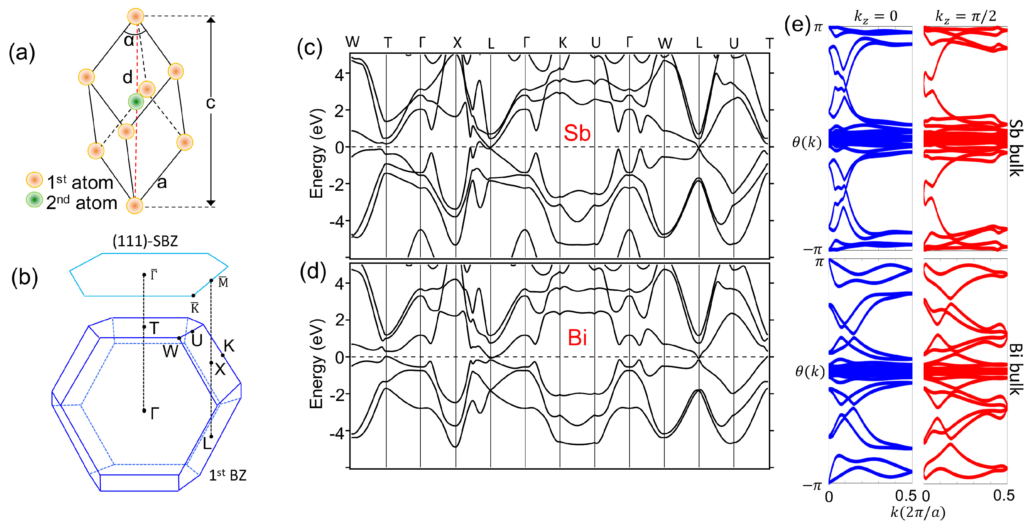
Abstract
1. Introduction
2. Experimental and Computational Methods
3. Band Structure of Bismuth and Antimony
4. ARPES Results and Calculated Bands of Thin Films
5. How to Reveal Bulk Band Topology in Thin Films
6. Strain-Induced Band Topology in Bismuth
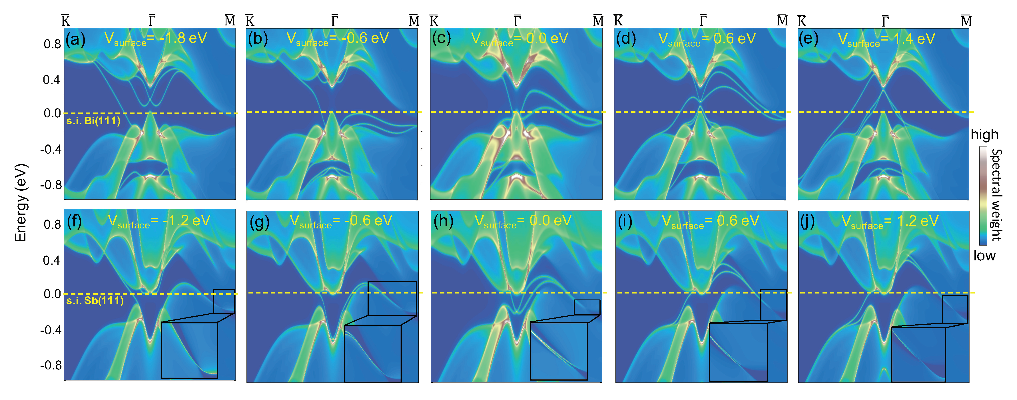
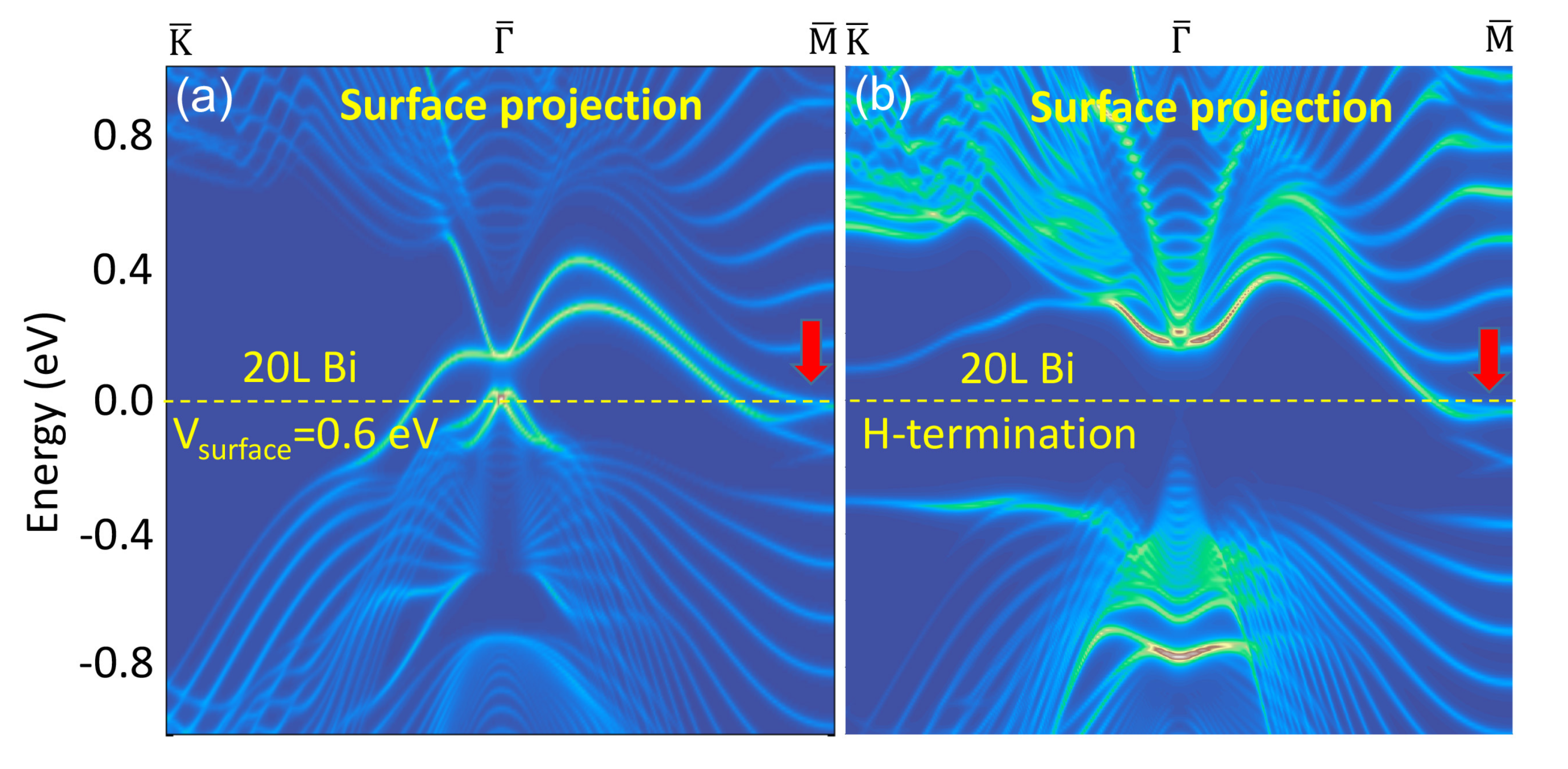
7. Surface Response as an Indicator of Band Topology
8. Conclusions
Author Contributions
Funding
Conflicts of Interest
References
- Hofmann, P. The surfaces of bismuth: Structural and electronic properties. Prog. Surf. Sci. 2006, 81, 191. [Google Scholar] [CrossRef]
- Koroteev, Y.M.; Bihlmayer, G.; Gayone, J.E.; Chulkov, E.V.; Blügel, S.P.; Echenique, M.; Hofmann, P. Strong Spin-Orbit Splitting on Bi Surfaces. Phys. Rev. Lett. 2004, 93, 046403. [Google Scholar] [CrossRef] [PubMed]
- Bian, G.; Wang, X.; Miller, T.; Chiang, T.-C.; Kowalczyk, P.J.; Mahapatra, O.; Brown, S.A. First-principles and spectroscopic studies of Bi(110) films: Thickness dependent Dirac modes and property oscillations. Phys. Rev. B 2014, 90, 195409. [Google Scholar] [CrossRef]
- Wang, G.; Pandey, R.; Karna, S.P. Atomically Thin Group V Elemental Films: Theoretical Investigations of Antimonene Allotropes. ACS Appl. Mater. Interfaces 2015, 7, 11490. [Google Scholar] [CrossRef] [PubMed]
- Ohtsubo, Y.; Kimura, S.-I. Topological phase transition of single-crystal Bi based on empirical tight-binding calculations. New J. Phys. 2016, 18, 123015. [Google Scholar] [CrossRef]
- Aguilera, I.; Friedrich, C.; Blügel, S. Electronic phase transitions of bismuth under strain from relativistic self-consistent GW calculations. Phys. Rev. B 2015, 91, 125129. [Google Scholar] [CrossRef]
- Hirahara, T. The Rashba and quantum size effects in ultrathin Bi films. J. Electron. Spectrosc. Relat. Phenom. 2015, 201, 98. [Google Scholar] [CrossRef]
- Hirahara, T.; Fukui, N.; Shirasawa, T.; Yamada, M.; Aitani, M.; Miyazaki, H.; Matsunami, M.; Kimura, S.; Takahashi, T.; Hasegawa, S.; et al. Atomic and Electronic Structure of Ultrathin Bi(111) Films Grown on Bi2Te3(111) Substrates: Evidence for a Strain-Induced Topological Phase Transition. Phys. Rev. Lett. 2012, 109, 227401. [Google Scholar] [CrossRef]
- Yao, M.-Y.; Zhu, F.; Han, C.Q.; Guan, D.D.; Liu, C.; Qian, D.; Jia, J.-F. Topologically nontrivial bismuth(111) thin films. Sci. Rep. 2016, 6, 21326. [Google Scholar] [CrossRef]
- Takayama, A.; Sato, T.; Souma, S.; Oguchi, T.; Takahashi, T. One-Dimensional Edge States with Giant Spin Splitting in a Bismuth Thin Film. Phys. Rev. Lett. 2015, 114, 066402. [Google Scholar] [CrossRef]
- Hirahara, T.; Miyamoto, K.; Matsuda, I.; Kadono, T.; Kimura, A.; Nagao, T.; Bihlmayer, G.; Chulkov, E.V.; Qiao, S.; Shimada, K.; et al. Direct observation of spin splitting in bismuth surface states. Phys. Rev. B 2007, 76, 153305. [Google Scholar] [CrossRef]
- Sugawara, K.; Sato, T.; Souma, S.; Takahashi, T.; Arai, M.; Sasaki, T. Fermi Surface and Anisotropic Spin-Orbit Coupling of Sb(111) Studied by Angle-Resolved Photoemission Spectroscopy. Phys. Rev. Lett. 2006, 96, 046411. [Google Scholar] [CrossRef] [PubMed]
- Ast, C.R.; Höchst, H. Fermi Surface of Bi(111) Measured by Photoemission Spectroscopy. Phys. Rev. Lett. 2001, 87, 177602. [Google Scholar] [CrossRef] [PubMed]
- Kowalczyk, P.J.; Mahapatra, O.; Brown, S.A.; Bian, G.; Wang, X.; Chiang, T.-C. Electronic Size Effects in Three-Dimensional Nanostructures. Nano Lett. 2013, 13, 43. [Google Scholar] [CrossRef] [PubMed]
- Hirahara, T.; Nagao, T.; Matsuda, I.; Bihlmayer, G.; Chulkov, E.V.; Koroteev, Y.M.; Echenique, P.M.; Saito, M.; Hasegawa, S. Role of Spin-Orbit Coupling and Hybridization Effects in the Electronic Structure of Ultrathin Bi Films. Phys. Rev. Lett. 2006, 97, 146803. [Google Scholar] [CrossRef] [PubMed]
- Hasan, M.Z.; Kane, C.L. Colloquium: Topological insulators. Rev. Mod. Phys. 2010, 82, 3045–3067. [Google Scholar] [CrossRef]
- Qi, X.-L.; Zhang, S.-C. Topological insulators and superconductors. Rev. Mod. Phys. 2011, 83, 1057–1110. [Google Scholar] [CrossRef]
- Hasan, M.Z.; Xu, S.-Y.; Bian, G. Topological insulators, topological superconductors and Weyl fermion semimetals: Discoveries, perspectives and outlooks. Phys. Scr. 2015, T164, 014001. [Google Scholar] [CrossRef]
- Bansil, A.; Lin, H.; Das, T. Colloquium: Topological band theory. Rev. Mod. Phys. 2016, 88, 021004. [Google Scholar] [CrossRef]
- Trivedi, T.; Roy, A.R.; Movva, H.C.P.; Walker, E.S.; Bank, S.R.; Neikirk, D.P.; Banerjee, S.K. Versatile Large-Area Custom-Feature van der Waals Epitaxy of Topological Insulators. ACS Nano 2017, 11, 7457. [Google Scholar] [CrossRef]
- Ueda, Y.; Khang, N.H.D.; Yao, K.; Hai, P.N. Epitaxial growth and characterization of Bi1−xSbx spin Hall thin films on GaAs(111)A substrates. Appl. Phys. Lett. 2017, 110, 062401. [Google Scholar] [CrossRef]
- Walker, E.S.; Na, S.R.; Jung, D.; March, S.D.; Kim, J.-S.; Trivedi, T.; Li, W.; Tao, L.; Lee, M.L.; Liechti, K.M.; et al. Large-Area Dry Transfer of Single-Crystalline Epitaxial Bismuth Thin Films. Nano Lett. 2016, 16, 6931. [Google Scholar] [CrossRef] [PubMed]
- Fu, L.; Kane, C.L.; Mele, E.J. Topological Insulators in Three Dimensions. Phys. Rev. Lett. 2007, 98, 106803. [Google Scholar] [CrossRef]
- Teo, J.C.Y.; Fu, L.; Kane, C.L. Surface states and topological invariants in three-dimensional topological insulators: Application to Bi1−xSbx. Phys. Rev. B 2008, 78, 045426. [Google Scholar] [CrossRef]
- Liu, Y.; Allen, R.E. Electronic structure of the semimetals Bi and Sb. Phys. Rev. B 1995, 52, 1566. [Google Scholar] [CrossRef] [PubMed]
- Lenoir, B.; Cassart, M.; Michenaud, J.-P.; Scherrer, H.; Scherrer, S. Transport properties of Bi-RICH Bi-Sb alloys. J. Phys. Chem. Solids 1996, 57, 89. [Google Scholar] [CrossRef]
- Kim, H.-J.; Kim, K.-S.; Wang, J.-F.; Sasaki, M.; Satoh, N.; Ohnishi, A.; Kitaura, M.; Yang, M.; Li, L. Dirac versus Weyl Fermions in Topological Insulators: Adler-Bell-Jackiw Anomaly in Transport Phenomena. Phys. Rev. Lett. 2013, 111, 246603. [Google Scholar] [CrossRef]
- Ohtsubo, Y.; Perfetti, L.; Goerbig, M.O.; Fèvre, P.L.; Bertran, F.; Taleb-Ibrahimi, A. Non-trivial surface-band dispersion on Bi(111). New J. Phys. 2013, 15, 033041. [Google Scholar] [CrossRef]
- Perfetti, L.; Faure, J.; Papalazarou, E.; Mauchain, J.; Marsi, M.; Goerbig, M.O.; Taleb-Ibrahimi, A.; Ohtsubo, Y. New aspects of electronic excitations at the bismuth surface: Topology, thermalization and coupling to coherent phonons. J. Electron. Spectrosc. Relat. Phenom. 2015, 201, 60. [Google Scholar] [CrossRef]
- Ito, S.; Feng, B.; Arita, M.; Takayama, A.; Liu, R.-Y.; Someya, T.; Chen, W.-C.; Iimori, T.; Namatame, H.; Taniguchi, M.C.-M.; et al. Proving Nontrivial Topology of Pure Bismuth by Quantum Confinement. Phys. Rev. Lett. 2016, 117, 236402. [Google Scholar] [CrossRef]
- Bian, G.; Miller, T.; Chiang, T.-C. Electronic structure and surface mediated metastability of Bi films on Si(111)-7x7 studied by angle resolved photoemission spectroscopy. Phys. Rev. B 2009, 80, 245407. [Google Scholar] [CrossRef]
- Yaginuma, S.; Nagao, T.; Sadowski, J.T.; Saito, M.; Nagaoka, K.; Fujikawa, Y.; Sakurai, T.; Nakayama, T. Origin of flat morphology and high crystallinity of ultrathin bismuth films. Surf. Sci. 2007, 601, 3593. [Google Scholar] [CrossRef]
- Bian, G.; Miller, T.; Chiang, T.-C. Passage from spin-polarized surface states to unpolarized quantum well states in topologically nontrivial Sb films. Phys. Rev. Lett. 2011, 107, 036802. [Google Scholar] [CrossRef]
- Bian, G.; Wang, X.; Liu, Y.; Miller, T.; Chiang, T.-C. Interfacial Protection of Topological Surface States in Ultrathin Sb Film. Phys. Rev. Lett. 2012, 108, 176401. [Google Scholar] [CrossRef] [PubMed]
- Kresse, G.; Joubert, J. From ultrasoft pseudopotentials to the projector augmented-wave method. Phys. Rev. B 1999, 59, 1758. [Google Scholar] [CrossRef]
- Kress, G.; Furthmüller, J. Efficiency of ab-initio total energy calculations for metals and semiconductors using a plane-wave basis set. Comput. Mater. Sci. 1996, 6, 15. [Google Scholar] [CrossRef]
- Souza, I.; Marzari, N.; Vanderbilt, D. Maximally localized Wannier functions for entangled energy bands. Phys. Rev. B 2001, 65, 035109. [Google Scholar] [CrossRef]
- Franchini, C.; Kovik, R.; Marsman, M.; Murthy, S.S.; He, J.; Ederer, C.; Kresse, G. Maximally localized Wannier functions in LaMnO3 within PBE + U, hybrid functionals and partially self-consistent GW: An efficient route to construct ab initio tight-binding parameters for eg perovskites. J. Phys. Condens. Matter 2012, 24, 235602. [Google Scholar] [CrossRef]
- Zhang, H.; Liu, C.-X.; Qi, X.-L.; Dai, X.; Fang, Z.; Zhang, S.-C. Topological insulators in Bi2Se3, Bi2Te3 and Sb2Te3 with a single Dirac cone on the surface. Nat. Phys. 2009, 78, 438–442. [Google Scholar] [CrossRef]
- Tsai, W.-F.; Huang, C.-Y.; Chang, T.-R.; Lin, H.; Jeng, H.-T.; Bansil, A. Gated silicene as a tunable source of nearly 100. Nat. Commun. 2013, 4, 1500. [Google Scholar] [CrossRef]
- Wang, Z.F.; Chen, L.; Liu, F. Tuning Topological Edge States of Bi(111) Bilayer Film by Edge Adsorption. Nano Lett. 2014, 14, 2879. [Google Scholar] [CrossRef]
- Yu, R.; Qi, X.-L.; Bernevig, A.; Fang, Z.; Dai, X. Equivalent expression of Z2 topological invariant for band insulators using the non-Abelian Berry connection. Phys. Rev. B 2011, 84, 075119. [Google Scholar] [CrossRef]
- Hsieh, D.; Xia, Y.; Wray, L.; Qian, D.; Pal, A.; Dil, J.H.; Osterwalder, J.; Meier, F.; Bihlmayer, G.; Kane, C.L.; et al. Observation of Unconventional Quantum Spin Textures in Topological Insulators. Science 2009, 323, 919–922. [Google Scholar] [CrossRef] [PubMed]
- Chiang, T.-C. Photoemission studies of quantum well states in thin films. Surf. Sci. Rep. 2000, 39, 181. [Google Scholar] [CrossRef]
- Zhang, Y.; He, K.; Chang, C.-Z.; Song, C.-L.; Wang, L.-L.; Chen, X.; Jia, J.-F.; Fang, Z.; Dai, X.; Shan, W.-Y.; et al. Crossover of the three-dimensional topological insulator Bi2Se3 to the two-dimensional limit? Nat. Phys. 2010, 6, 584. [Google Scholar] [CrossRef]
- Zhou, X.; Hsu, C.-H.; Chang, T.-R.; Tien, H.-J.; Ma, Q.; Jarillo-Herrero, P.; Gedik, N.; Bansil, A.; Pereira, V.M.; Xu, S.-Y.; et al. Opological crystalline insulator states in the Ca2As family. Phys. Rev. B 2018, 98, 241104(R). [Google Scholar] [CrossRef]
- Hsu, C.-H.; Zhou, X.; Ma, Q.; Gedik, N.; Bansil, A.; Pereira, V.M.; Lin, H.; Fu, L.; Xu, S.-Y.; Chang, T.-R. Purely Rotational Symmetry-Protected Topological Crystalline Insulator α-Bi4Br4. 2D Mat. 2019, 6, 031004. [Google Scholar] [CrossRef]
- Bian, G.; Wang, X.; Miller, T.; Chiang, T.-C. Topological phase transition and Dirac fermion transfer in Bi2Se3 films. EPL 2013, 101, 27004. [Google Scholar] [CrossRef]
- Bian, G.; Zhang, L.; Liu, Y.; Miller, T.; Chiang, T.-C. Detecting Spin Texture of Bi/Ag Surface Alloy by Circular Angular Resolved Photoemission Spectroscopy. Phys. Rev. Lett. 2012, 108, 186403. [Google Scholar] [CrossRef] [PubMed]
- Bian, G.; Wang, Z.F.; Wang, X.; Xu, C.; Xu, S.-Y.; Miller, T.; Hasan, M.Z.; Liu, F.; Chiang, T.-C. Engineering electronic structure of a 2D topological insulator Bi(111) bilayer on Sb nanofilms by quantum confinement effect. ACS Nano 2016, 10, 3859. [Google Scholar] [CrossRef] [PubMed]


© 2019 by the authors. Licensee MDPI, Basel, Switzerland. This article is an open access article distributed under the terms and conditions of the Creative Commons Attribution (CC BY) license (http://creativecommons.org/licenses/by/4.0/).
Share and Cite
Chang, T.-R.; Lu, Q.; Wang, X.; Lin, H.; Miller, T.; Chiang, T.-C.; Bian, G. Band Topology of Bismuth Quantum Films. Crystals 2019, 9, 510. https://doi.org/10.3390/cryst9100510
Chang T-R, Lu Q, Wang X, Lin H, Miller T, Chiang T-C, Bian G. Band Topology of Bismuth Quantum Films. Crystals. 2019; 9(10):510. https://doi.org/10.3390/cryst9100510
Chicago/Turabian StyleChang, Tay-Rong, Qiangsheng Lu, Xiaoxiong Wang, Hsin Lin, T. Miller, Tai-Chang Chiang, and Guang Bian. 2019. "Band Topology of Bismuth Quantum Films" Crystals 9, no. 10: 510. https://doi.org/10.3390/cryst9100510
APA StyleChang, T.-R., Lu, Q., Wang, X., Lin, H., Miller, T., Chiang, T.-C., & Bian, G. (2019). Band Topology of Bismuth Quantum Films. Crystals, 9(10), 510. https://doi.org/10.3390/cryst9100510